
Related Manuals for Panasonic KX-NS500AG


Summary of Contents for Panasonic KX-NS500AG
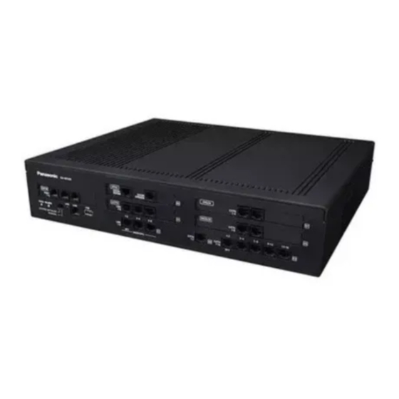
- Page 1 ORDER NO. KMS1409096CE Hybrid IP-PBX KX-NS500AG Model No. (for Argentina) © Panasonic System Networks Co., Ltd. 2014 Unauthorized copying and distribution is a violation of law.
-
Page 2: Table Of Contents
KX-NS500AG TABLE OF CONTENTS PAGE PAGE 1 Safety Precautions -----------------------------------------------4 10.1. Mother Board and CPU Board ----------------------- 36 1.1. For Service Technicians ---------------------------------4 10.2. Fan and Power Supply Board ------------------------ 37 11 Miscellaneous --------------------------------------------------- 38 1.2. Insulation Resistance Test -------------------------------4 11.1. - Page 3 KX-NS500AG 13.4. Memo --------------------------------------------------------94 13.5. Power Supply Board -------------------------------------94 13.5.1. Component View-------------------------------------94 13.5.2. Bottom View-------------------------------------------95 14 Appendix Information of Schematic Diagram ---------96 15 Exploded View and Replacement Parts List -----------97 15.1. IC Date ------------------------------------------------------97 15.1.1. IC400 ---------------------------------------------------97 15.1.2. IC401 ---------------------------------------------------99 15.1.3.
-
Page 4: Safety Precautions
KX-NS500AG 1 Safety Precautions 1. Before servicing, unplug the AC power cord to prevent an electric shock. 2. When replacing parts, use only the manufacturer's recommended components. 3. Check the condition of the power cord. Replace if wear or damage is evident. -
Page 5: About Lead Free Solder (Pbf: Pb Free)
KX-NS500AG 2.3. About Lead Free Solder (PbF: Pb free) Note: In the information below, Pb, the symbol for lead in the periodic table of elements, will refer to standard solder or solder that con- tains lead. We will use PbF when discussing the lead free solder used in our manufacturing process which is made from Tin, (Sn), Silver, (Ag), and Copper, (Cu). -
Page 6: Specifications
KX-NS500AG 3 Specifications 3.1. General Description Main CPU Cortex A8 600 MHz Power Input 100 V AC to 130 V AC: 2.2 A/200 V AC to 240 V AC: 1.3 A;50 Hz/60 Hz Power Consumption (when fully mounted) 110 W External Backup Battery External battery port is not supported. -
Page 7: Technical Descriptions
KX-NS500AG 4 Technical Descriptions 4.1. Block Diagram The NS500 series PBX is constructed in Main Unit (NS500) and up to three expansion unit (NS520). In Main Unit (NS500), CPU Board (MPR) (Master Processor) which controlls whole call of this system is equipped, and, in an expansion unit, CPU Board (SPR) (Slave Processor) controlling various line interfaces in the unit is equipped with. - Page 8 KX-NS500AG Table.3 Main Unit Option Card Description Card Description SD(L/M/S) SD card is used for strage memory of UM. SD card is implemented on CPU Board (MPR) . The capacity of SD card are: SD(M):16GB§SD(L):8GB§SD(XS):2GB In the case of NS500, it is necessary to implement it when using a VoIP functions.
-
Page 9: Main Unit
KX-NS500AG 4.2. Main Unit The Main Unit is constructed by CPU Board (MPR) and Mother Board. The block diagram and operation of each card are described here. 4.2.1. CPU Board (MPR) Fig.2 shows detail block diagram of CPU Board (MPR) , and each function of CPU Board (MPR) is described in Table.4. -
Page 10: Main Unit Mother Board
KX-NS500AG 4.2.2. Main Unit Mother Board Fig.3 shows detail block diagram of Mother Board, and each function of Base is described in Table.5. SLIC/CODEC bus (SPI) SLIC/CODEC(2ch) INT(2) RJ45 INT_SLIC PLD1 SLIC/CODEC(2ch) INT_EXT ( EXT_PLD) INT_CO SLIC/CODEC(2ch) IIO bus RJ45... -
Page 11: Expansion Unit
KX-NS500AG 4.3. Expansion Unit The expansion unit is constructed by CPU Board (SPR) and Mother Board. The block diagram and operation of each card are described here. 4.3.1. CPU Board (SPR) Fig.4 shows detail block diagram of CPU Board (SPR), and each function of CPU Board (SPR) is described in Table.6. -
Page 12: Expansion Unit Mother Board
KX-NS500AG 4.3.2. Expansion Unit Mother Board Fig.5 shows detail block diagram of Mother Board, and each function of Base is described in Table.7. SLIC/CODEC bus (SPI) SLIC/CODEC(2ch) INT(2) RJ45 INT_SLIC PLD1 SLIC/CODEC(2ch) INT_EXT (EXT_PLD) INT_CO SLIC/CODEC(2ch) RJ45 SLIC/CODEC(2ch) SLIC/CODEC(2ch) RJ45... -
Page 13: Power Circuit
KX-NS500AG 4.4. Power Circuit Fig.6 shows power circuit diagram of NS500. In AC/DC convert blotck, AC input voltage is converted to DC+15V and DC+41V. DC+15V/+41V is distributed to each card. +41 V Extension#1 Extension#2 +15 V 15V/3.3V AC/DC Base Trunk#1... -
Page 14: Power Supply Unit
KX-NS500AG 4.5. Power Supply Unit This unit is switching regulator power supply and supplies DC voltages to DCPU Board (MPR), and optional card (free slot). PSU (power supply unit) has two outputs (41V, 15V). 15V output is supplied only in DCPU Board (MPR) and option card. Other outputs are mainly used as an object for the electric supply to a terminal. -
Page 15: Main Converter
KX-NS500AG 2) Rectification Smoothing Circuit This circuit consists mainly of the following components and performs DC-AC conversion. D1: Diode Bridge C5: Primary Smoothing Condenser 3) Surge Absorber Circuit As the main component of this circuit, Z1 protects against exogenous noise such as lightning surge. -
Page 16: Output Voltage
KX-NS500AG 3) Latch Circuit The main converter latch circuit works to prevent output voltage from reaching an abnormally high state. This circuit uses mainly the latch function of IC1. When secondary side protection circuit reaches an abnormal state (section 6 protection circuit), the signal is sent to primary side through PC50. - Page 17 KX-NS500AG 2) 41V Output voltage 2-1) 41V Output FET Q151 is in ON status during normal operation, conducts to main converter output and the potentiostatically-controlled volt- age is output. Q151 is in ON status when the sub winding voltage of coil L201 of 15V output converter has force applied to it.
-
Page 18: Battery Voltage Input And Output
KX-NS500AG 4.9. Battery voltage input and output This section describes the operation of battery input and output. 1) Battery voltage output (charge time) Charge circuit has constant voltage and constant current. When the battery voltage is high, a controlled fixed voltage of the main converter is output. -
Page 19: Alarm Signal Sending Circuit
KX-NS500AG 4.10. Alarm Signal Sending Circuit This section describes the operation of the circuit that sends the AC alarm/DC alarm signal 1) Alarm Circuit Power Supply This power supply consists mainly of Q301, D301. The output of the main converter (described in section 2) drops from 41V to around 26V for a more stable supply. -
Page 20: Protection Circuit
KX-NS500AG 4.11. Protection Circuit This section describes the Overvoltage Protection Circuit and Overheat Protection Circuit. 1) Abnormal Condition Detection Circuit Abnormal condition detection circuit is a thyristor circuit which is comprised of Q306 and Q307. When power supply operation becomes abnormal, a signal is sent to the abnormal detection circuit and Q307 is turned ON. A current flows through the diode of PC50, which is sent to the control circuit of main converter. -
Page 21: Location Of Controls And Components
KX-NS500AG 5 Location of Controls and Components 5.1. Name and Locations... -
Page 22: Installation Instructions
KX-NS500AG 6 Installation Instructions 6.1. System Components Refer to 16. Appendix (P.131). 7 Operating Instructions 7.1. System Capacity Refer to 16. Appendix (P.131). 8 Test Mode 8.1. Utillity Refer to16. Appendix (P.131). -
Page 23: Troubleshooting Guide
KX-NS500AG 9 Troubleshooting Guide IMPORTANT NOTICE CPU Board (MPR) NS300/500 CPU Board (MPR) has battery backuped SRAM, and this SRAM is supplied by battery which is equipped on Mother board. Once CPU Board (MPR) is removed from Mother board, Mother Board 'System Initialization' is required. -
Page 24: Startup
KX-NS500AG 9.1.1. Startup... - Page 25 KX-NS500AG...
- Page 26 KX-NS500AG...
- Page 27 KX-NS500AG...
-
Page 28: Battery Alarm
KX-NS500AG 9.1.2. Battery Alarm... -
Page 29: Using Voice Mail
KX-NS500AG 9.1.3. Using Voice Mail... - Page 30 KX-NS500AG Using Voice Mail (continued)
-
Page 31: Others
KX-NS500AG 9.1.4. Others 9.1.5. SLIC/CODEC (SLC) Block Refer to Service Manual of KX-NS5173/KX-NS5174. 9.1.6. DSP (LCOT) Block Refer to Service Manual of KX-NS5180. 9.1.7. DPT I/F Block Refer to Service Manual of KX-NS5170/KX-NS5171/KX-NS5172. -
Page 32: Power Supply
KX-NS500AG 9.2. Power Supply 9.2.1. No Voltage is Output at All (1) Main converter output voltage error [C102]... -
Page 33: No Voltage Is Output At All (2)
KX-NS500AG 9.2.2. No voltage is Output at All (2) (Output voltage of Main Converter is Normal (C101, C102)) -
Page 34: Are Not Output
KX-NS500AG 9.2.3. 41V are Not Output (Only 15V is output) -
Page 35: Battery Backup Function Does Not Operate / Psu Can Not Charge Batteries
KX-NS500AG 9.2.4. Battery Backup Function Does Not Operate / PSU can Not Charge Batteries... -
Page 36: Disassembly And Assembly Instructions
KX-NS500AG 10 Disassembly and Assembly Instructions 10.1. Mother Board and CPU Board 1. Loosen the 3 Screws (B). 2. Side the Top Cover in the direction shown below (1). 3. Removet the Top Cover. 4. Loosen the 3 Screws (A and E) and Spacer. -
Page 37: Fan And Power Supply Board
KX-NS500AG 10.2. Fan and Power Supply Board 1. Loosen the 1 Screws(A), Remove the Fan Cover. 2. Remove the DC Motor. 3. Remove the 1connector from the Mother Board. 4. Loosen the 2 Screws(A) and 2 Screws(E), Remove the Capacitor Cover. -
Page 38: Miscellaneous
KX-NS500AG 11 Miscellaneous 11.1. How To Replace a Flat Package IC Even if you do not have the special tools (for example, a spot heater) to remove the Flat IC, with some solder (large amount), a sol- dering iron and a cutter knife, you can easily remove the ICs that have more than 100 pins. -
Page 39: How To Replace The Llp (Leadless Leadframe Package) Ic And Ic Ground Plate
KX-NS500AG 11.2. How to Replace the LLP (Leadless Leadframe Package) IC and IC ground plate 11.2.1. Preparation • PbF (: Pb free) Solder • Soldering Iron Tip Temperature of 700 F ± 20 F (370 C ± 10 C) Note: We recommend a 30 to 40 Watt soldering iron. -
Page 40: How To Remove A Solder Bridge (Doesn't Apply To Ic Ground Plate.)
KX-NS500AG 11.2.5. How to Remove a Solder Bridge (Doesn't apply to IC ground plate.) When a Solder Bridge is found after soldering the bottom of the IC, remove it with a soldering iron. -
Page 41: Terminal Guide Of The Ics, Transistors And Diodes
KX-NS500AG 11.3. Terminal Guide of the ICs, Transistors and Diodes 11.3.1. Mother Board C0JBAB000535 C0ABBB000179 C2HBBY000149 PNWI2NS300BX C1CB00003834 C0JBAZ002713 C1ZBZ0005171 C0JBAB000551 DSC7003S0L C0BBBA000022 C1ZBZ0005172 DSA7003R0L C0DBAYY01692 B1ABGE000014 DMG504010R B1ADGE000012 B1CHRE000013 B1HBCFA00006 B1CFRM000027 B0ADDH000005 Cathode Anode B1GFAFNN0001 XP4401 B0KB00000087 DA3J101F0L PQVDPTZT2524... -
Page 42: Cpu Board
KX-NS500AG 11.3.2. CPU Board AB22 C0BBBA000022 C1ZBZ0004359 C1ZBZ0005132 C3FBMY000318 C2DBYY001353 C3ABUY000061 C0DBEYY00232 C0JBAB000785 C0JBAB000551 C0JBAE000285 C3BBKY000079 C1CB00003913 C0DBZYY00444 PNWI1S500AG1 C0JBAA000319 C0DBAYY00932 C0JBAZ002713 C0DBZYY00702 C0DBAYY01566 B1CHRE000013 C0DBAYY00903 C0JBAA000244 C0DBAYY01581 Anode Cathode Anode Cathode DB2J31400L B3AGB0000050 B3ABB0000403 DMG504010R B0JCDD000018 Cathode Anode DZ2J062M0L... -
Page 43: Power Supply Board
KX-NS500AG 11.3.3. Power Supply Board... -
Page 44: Schematic Diagram
C112B VIN[1] (14) T100B R118B Q100B 0.1u 50 R113B 100k TH100B R104B R122B 100k RL100B C109B J100B SFGA +3.3V RL101B +3.3V R171B R110B DP[1] (15) SHUNT[1] SHUNT[1] (16) J102 C130 1000p C140 J100 C131 1000p KX-NS500AG MOTHER BOARD No.1 1/2... - Page 45 EGPIO4/SEG28/HDB0 nCS_DSPG[0] HW_CLK[1] BGPIO11/SEG3/SCLK/SLOTINT/SYNCMATCH AGPIO9/SEG27/CA9/SIODO0/UCFG0 HW_FH[1] BGPIO12/SEG4/FSYNC/RXBITCLK AGPIO8/SEG26/CA8/SIODI0 BGPIO13/SEG5/DL0/RXDATA AGPIO7/SEG25/CA7/SIOCLK0 LDHW[1] BGPIO15/SEG6/CLKOUT0 AGPIO6/SEG24/CA6/PWM5/BP CGPIO2/SEG6/EXTINT2 AGPIO5/SEG23/CA5/PWM4 (10) CGPIO3/SEG7/EXTINT3/[RFCTL4/SHCTRL] AGPIO4/SEG22/CA4/PWM3/TEST CGPIO4/SEG8/ANT0 AGPIO3/SEG21/CA3/PWM2 (11) R153A nREAD nWRITE nRST_CO (12) DP[1] DP[0] (13) REVDET[0-5] BELL[0-5] (14) DP[1] (15) (16) KX-NS500AG MOTHER BOARD No.1 2/2...
- Page 46 R115D D109D C139D R116D IC100D 100p PC103D 8.2k +3.3V C112D D104D VIN[3] (14) T100D R118D Q100D 0.1u 50 R113D 100k TH100D R104D R122D 100k RL100D C109D J100D SFGC +3.3V RL101D +3.3V R171D R110D (15) (16) KX-NS500AG MOTHER BOARD No.2 1/2...
- Page 47 BGPIO11/SEG3/SCLK/SLOTINT/SYNCMATCH AGPIO9/SEG27/CA9/SIODO0/UCFG0 HW_CLK[1] BGPIO12/SEG4/FSYNC/RXBITCLK AGPIO8/SEG26/CA8/SIODI0 HW_FH[1] BGPIO13/SEG5/DL0/RXDATA AGPIO7/SEG25/CA7/SIOCLK0 LDHW[1] BGPIO15/SEG6/CLKOUT0 AGPIO6/SEG24/CA6/PWM5/BP CGPIO2/SEG6/EXTINT2 AGPIO5/SEG23/CA5/PWM4 (10) CGPIO3/SEG7/EXTINT3/[RFCTL4/SHCTRL] AGPIO4/SEG22/CA4/PWM3/TEST CGPIO4/SEG8/ANT0 AGPIO3/SEG21/CA3/PWM2 (11) R153C nREAD nWRITE nRST_CO (12) DP[3] DP[2] (13) REVDET[0-5] BELL[0-5] (14) DP[3] (15) SHUNT[3] (16) KX-NS500AG MOTHER BOARD No.2 2/2...
- Page 48 56p 50 IC100F C139F R116F PC103F 100p +3.3V 8.2k C112F (14) D104F T100F R118F Q100F 0.1u 50 R113F 100k TH100F R104F R122F 100k C109F J100F SFGE +3.3V RL101F R171F RL100F +3.3V R110F (15) SHUNT[5] SHUNT[5] (16) KX-NS500AG MOTHER BOARD No.3 1/2...
- Page 49 BELL[5] nWRITE (12) nREAD DP[5] DP[4] VOUT[5] (13) REVDET[0-5] BELL[0-5] VIN[5] (14) R137 DSPG_CLK +3.3V DL100 R135 13.824MHz 1 1A 2 3Y DP[5] 3 2A R132 (15) 4 GND (16) IC104 TP412 13.824M X100 KX-NS500AG MOTHER BOARD No.3 2/2...
- Page 50 R210D R211D 1.65MF VDDD RINGB C211C VDDREG 0.22u 0.1u TIPB Q200D R205D +3.3V R220D R200D R206D C207D 0.01u R207D 681kF RL200D R208D C208D 0.01u PF_TD R221D R209D 681kF R201D SLIC_DOUT SLIC_DIN RL200D SLIC_CLK[0] nSLIC_CS[1] PF_RD KX-NS500AG MOTHER BOARD No.4 1/2...
- Page 51 SDCHB L200H 100u C204H L201H 100u R210H R211H 1.65MF VDDD RINGB C211G VDDREG 0.22u 0.1u TIPB Q200H R205H +3.3V R200H R206H C207H 0.01u R207H 681kF SLIC_DOUT R208H C208H SLIC_DIN 0.01u R209H 681kF SLIC_CLK[0] R201H nSLIC_CS[3] KX-NS500AG MOTHER BOARD No.4 2/2...
- Page 52 L201L 100u R210L R211L 1.65MF VDDD RINGB C 2 1 1 K VDDREG 0.1u 0.22u TIPB Q200L R205L +3.3V R200L R206L C207L 0.01u R207L 681kF R208L C208L 0.01u R209L 681kF R201L SLIC_DOUT SLIC_DIN SLIC_CLK[1] nSLIC_CS[5] KX-NS500AG MOTHER BOARD NO.5 1/2...
- Page 53 SDCHB L200P 100u C204P L201P 100u R210P R211P 1.65MF VDDD RINGB C211O VDDREG 0.22u 0.1u TIPB Q200P R205P +3.3V C207P R200P R206P 0.01u R207P 681kF C208P R208P SLIC_DOUT 0.01u R209P 681kF SLIC_DIN R201P SLIC_CLK[1] nSLIC_CS[7] KX-NS500AG MOTHER BOARD NO.5 2/2...
- Page 54 +3.3V R600 IC601 +3.3V R602 1 NC R613 R616 2.2k R614 3 GND DC_ALM C615 0.1u C616 Low Active 0.1u 1 NC R615 2.2k 3 GND AC_ALM IC602 R643 +15V R611 +3.3V CN601 R619 FAN_ALM KX-NS500AG MOTHER BOARD NO.6 1/2...
- Page 55 PT_RXB[1] R316B R318B R314B 1.5k C305B 1000p C303B U303B PT_TXB[0] PT_TXB[1] IC600 +3.3V 1 EN C607 2 VFB VBST L600 2.2u GND2 3 VREG5 0.1u 4 SS GND1 +3.3V R621 R622 R640 R641 R642 R636 KX-NS500AG MOTHER BOARD NO.6 2/2...
- Page 56 PT_CURB PT_POWB (43) CN401 CN401 nINT_CO[0] (44) nINT_CO[1] (45) CN401 CN401 (46) (47) CN401 CN401 (48) nRST_SLIC CN401 CN401 (49) +40V_OP (50) CN401 CN401 (51) (52) CN401 CN401 (53) (54) AC_ALM RING_SYNC (55) HW_CLK[2-6] nHW_FH[2-6] KX-NS500AG MOTHER BOARD No.7 1/3...
- Page 57 C424 0.1u 10 (39) C425 0.1u 10 (40) TP401 (41) (42) (43) (44) (45) (46) (69) (47) (70) (48) (71) R586 (49) 2.2k (50) (72) L_D[0-7] (51) (73) (52) (53) (74) (54) (75) (55) KX-NS500AG MOTHER BOARD No.7 2/3...
- Page 58 L_D[0] L_A[0] R573 L_A[2] L_A[4] L_D[7] L_A[6] L_D[5] L_D[3] R543 L_D[1] L_A[1] R574 L_A[3] L_A[5] L_A[7] R544 L_A[8] L_A[10] L_A[20] L_A[22] R545 L_A[9] L_A[11] L_A[21] R546 (69) (70) (71) L_A[0-22] (72) (73) L_D[0-7] (74) (75) KX-NS500AG MOTHER BOARD No.7 3/3...
-
Page 59: Memo
KX-NS500AG 12.2. Memo... -
Page 60: Cpu Board
VSS5 F2 VSS6 F8 VSS7 J1 VSS8 J9 VSS9 L1 VSS10 L9 VSS11 N1 VSS12 N9 VSSQ1 B2 VSSQ2 B8 VSSQ3 C9 VSSQ4 D1 VSSQ5 D9 NT5CB256M8FN-DI (10) (11) (12) (13) (14) (15) (16) (17) (18) KX-NS500AG CPU BOARD No.1 1/2... - Page 61 0.1u 16 C113 DDR_A[15] R111 (15) DDR_A[10] 0.1u 16 (16) DDR_A[12] C128 (17) DDR_A[7] R108 0.1u 16 (18) DDR_A[13] R112 DDD3 CLK DDR_A[9] DDR_A[0] R103 49.9 1 C111 R104 49.9 1 0.1u 16 DDD3 nCLK KX-NS500AG CPU BOARD No.1 2/2...
- Page 62 NAND ALE (17) +15V NAND RDY +3.3VD +3.3VD TP_+3.3VD_B +3.3VD_B D201 +3.3VD IC202 R236 2.2k +3.3VD 1SS424(TPH3,F) IC202 NJM2903M(TE1) D202 D203 TP_BAT_ALM R201 R230 0 +3.3V_BASE_BAT IC202 TP_3.3V_BAT BAT_ALM_n R238 R202 NJM2903M(TE1) 003:2D R232 R234 R241 KX-NS500AG CPU BOARD No.2 1/2...
- Page 63 +15V GP_A[16] GP_A[11] 20 A15 GP_A[15] 21 A14 GP_A[12] GP_A[14] 22 A13 GP_A[13] GP_A[0-21] 005:3C GP_A[0-21] SRAM *WE SRAM D[8] EM643FV16FU-55LF (12) nRD 005:4F (13) (14) nWE 005:4E (15) (16) GP_D[0-7] GP_D[0-7] 005:3B GP_D[0-15] (17) KX-NS500AG CPU BOARD No.2 2/2...
- Page 64 006:6E PMIC_RTC_nPOR A12 TCK 002:2B CPU_TCK B11 TDI 002:2B CPU_TDI A11 TDO 002:2B CPU_TDO C11 TMS 002:2B CPU_TMS A3 TESTOUT +1.8V_VPLL R301 A9 VREFN B9 VREFP I-AM3352ZCZ60-3 +3.3VD AM3352BZCZ60 R302 Initialize SW301 SK-12D26-G6.5NS normal initial KX-NS500AG CPU BOARD No.3 1/2...
- Page 65 (30) R344 R345 R346 L302 TP_DG7 JK302 LF301 (31) (32) (33) IC306 20201-3K16-01 (34) 1 IO1 +3.3VD 2 GND 3 IO2 (35) L301 IC304 BLM18PG181SN1D +5VD_USB R388 1 OUT 2 GND 3 *FLT ON/*ON AAT4614IGU-2-T1 KX-NS500AG CPU BOARD No.3 2/2...
- Page 66 R430 IO70 3 2A IO71 003:3E TDM0_CK_CPU IO72 4 GND TDM0_HCK_CPU 003:3E IO73 003:3E TDM0_DX_CPU IO74 TC7WZU04FK(TE85L,F TDM0_DR_CPU IO75 003:3E 003:3E TDM0_FS_CPU IO76 R424 I-EP4CE40F23C8N-2 +3.3VD X401 GND1 C411 1000p GND2 16.384M C409 0.1u 16 KX-NS500AG CPU BOARD No.4 1/2...
- Page 67 IO242 IO243 IO244 IO245 IO246 IO247 IO248 IO249/PADD0 IO250 IO251 IO252 IO253 IO254/PADD1 IO255/PADD2 IO256 IO257 IO258 IO259/PADD3 IO260/PADD4 IO261/PADD5 IO262/PADD6 IO263/PADD7 CPU_CARD_ID IO264/PADD8 IO265 IO266/PADD9 IO267/PADD10 IO268/PADD11 IO269/PADD12 IO270 IO271/PAD13 IO272/PAD14 CLK8 CLK9 I-EP4CE40F23C8N-7 KX-NS500AG CPU BOARD No.4 2/2...
- Page 68 (22) GP_BUF_A[6] F19 IO221 G18 IO222/PADD23 TC74LCX245FT(EKJ) GP_BUF_A[5] H17 IO223 GP_BUF_A[4] C22 IO224 GP_BUF_A[3] C21 IO225 BASE_BUFFER B22 IO226/PADD22 B21 IO227/PADD21 /(FPGA_ADDRESS_BUFFER) C20 IO228/PADD20 GP_BUF_A[2] D20 IO229 GP_BUF_A[1] F17 IO230 GP_BUF_A[0] G17 IO231 I-EP4CE40F23C8N-6 EP4CE40F23C8N KX-NS500AG CPU BOARD No.5 1/2...
- Page 69 GP_BUF_A[8] GP_BUF_A[7] R530 R531 GP_BUF_A[10] GP_BUF_A[9] CN501 77 A[10] CN501 A[9] GP_BUF_A[20] GP_BUF_A[11] GP_BUF_A[22] GP_BUF_A[21] CN501 78 A[20] CN501 A[11] CN501 79 CN501 A[22] A[21] CN501 80 CN501 GP_BUF_A[0-13,20-23] (18) (19) GP_BUF_D[0-7] (20) (21) (22) KX-NS500AG CPU BOARD No.5 2/2...
- Page 70 C16 GND35 VCCD_PLL1 GNDA3 0.1u 0.1u 16 U4 VCCIO2_2 VCCD_PLL2 GNDA4 C669 C664 2.2u 6.3 C688 W4 VCCIO2_3 VCCD_PLL3 0.1u I-EP4CE40F23C8N-9 0.1u 16 R4 VCCIO2_4 VCCD_PLL4 C670 C689 1.2V 0.1u 0.1u 16 I-EP4CE40F23C8N-10 C671 0.1u KX-NS500AG CPU BOARD No.6 1/2...
- Page 71 R649 F14 VDDSHV6_5 LCD(GPMC) IC604 G14 VDDSHV6_6 R614 N5 VDDSHV6_7 PWRONRSTn P5 VDDSHV6_8 USB_DRVVBUS C626 P6 VDDSHV6_9 WARMRSTn SN74LVC08APWR 0.01u 50 M5 VPP N.C. IC604 I-AM3352ZCZ60-4 SN74LVC08APWR 7 IC604 R650 L2SW_CLK_25MHz L2SW_CLK_BUF_25MHz 005:2A 003:6B SN74LVC08APWR KX-NS500AG CPU BOARD No.6 2/2...
-
Page 72: Relay Board
POWER SUPPLY SIDE PIN ASIGN +15V +15V +15V +15V +15V +15V 3W DUMMY REG. +15V +15V +15V +41V +15V +41V DC-ALM AC-ALM +41V +41V +41V +41V +41V +41V +41V +41V +41V +41V AC-ALM DC-ALM AC-ALM DC-ALM KX-NS500AG RELAY BOARD 1/1... -
Page 73: Memo
KX-NS500AG 12.5. Memo... -
Page 74: Power Supply Board
KX-NS500AG 12.6. Power Supply Board R221 R222 R223 1/10W 39k 1/10W 39k 1/10W 5.6k 50V 2700uF C205 C221 50V 4700pF 50V 2700uF C204 J203 J204 C203 C202 D201 D202 C201 C102 50V 2700uF C101 50V 560uF C501 630V 0.047uF 2kV 100pF... - Page 75 KX-NS500AG R328 1/8W 10k PC50 R324 R325 R323 1/10W 10k 1/10W 4.7k 1/8W 10k PTC301 1/8W 5.6k C312 C306 C307 R326 C301 25V 1uF 25V 1uF 50V 27uF R321 1/8W 4.7k 1/10W 10k R320 1/10W 4.7k R322 D313 D312 D301...
- Page 76 KX-NS500AG C167 C165 4700pF 4700pF C163 C162 C502 D169 D167 D168 630V 0.047uF R169 1/8W 1k C154 50V 330uF R167 1/8W 100k R158 1/10W 180k D164 C153 C161 50V 470pF R177 R159 50V 0.1uF R178 1/8W 0 1/8W 0 1/8W 33k...
- Page 77 KX-NS500AG PC80 1/10W 100k R344 1/10W 4.7k R345 C311 25V 4.7uF C310 10V 2.2uF C309 25V 1uF R340 D320 R346 1/10W 4.7k 1/8W 100k R339 1/8W 47k D315 R338 1/10W 15k R336 1/10W 15k R333 R332 1/8W 15k 1/8W 15k...
-
Page 78: Waveform
KX-NS500AG 12.7. Waveform 12.7.1. CPU Board Voltage DC-DC / LDO Voltage Spec Signal Name Specification [V] TP_+15V TP_+5VD TP_+3.3VD TP_+5VD_USB TP_1.1V_CORE +1.1V_MPU +1.8V_VDAC +1.5V_DDR +3.3V_VMMC +3.3V_VAUX2 +1.8V_VRTC +1.8V_PLL +1.8V_VAUX1 +1.8V_VDIG2 +3.3V_VAUX33 +1.2VD +2.5VD +1.8V_LAN TP_DDR_VREF 0.75 TP_DDR_VTT 0.75 +1.8V_VDAC +2.5VD +3.3V_VAUX3... - Page 79 KX-NS500AG DC-DC/LDO Output Voltage Signal Ripple Signal Ripple Waveform Waveform Name [mV] Name [mV] +5VD 70.8 +1.8V_VDAC 59.3 +3.3VD 42.7 +1.5V_DDR 86.4 +5VD_USB 36.4 +3.3V_VMMC 111.0 +1.1V_CORE 43.7 +3.3V_VAUX2 60.4 +1.1V_MPU 59.3 +1.8V_VRTC 38.5...
- Page 80 KX-NS500AG Signal Ripple Signal Ripple Waveform Waveform Name [mV] Name [mV] +1.8V_VPLL 73.9 +2.5VD 35.4 +1.8V_VAUX1 36.4 +1.8V_LAN 59.3 +1.8V_VDIG2 36.4 DDR_VREF 57.2 +3.3V_ 44.7 DDR_VTT 63.4 VAUX33 +1.2VD 43.7...
-
Page 81: Cpu Board Reset Signal
KX-NS500AG 12.7.2. CPU Board Reset Signal Reset Signal and Clock Description Signal Name Test Point Waveform DC+15V Input vs +15V TP_+15V DC-DC Output +5VD TP_+5VD (5V/3.3V) +3.3VD TP_+3.3VD 15.4ms DC+5V vs Reset +15V TP_+15V Timing +5VD TP_+5VD PORZ R647 20.2ms... - Page 82 KX-NS500AG Description Signal Name Test Point Waveform DC+5V vs +5VD TP_+5VD DC+1.8V_VPLL PORZ R647 +1.8V_VPLL TP_+1.8V_VPLL 9.5ms DC+5V vs +5VD TP_+5VD DC+1.5V_DDR PORZ R647 +1.5V_DDR TP_+1.5V_DDR 11.6ms DC+5V vs +5VD TP_+5VD DC+1.8V_VAUX PORZ R647 +1.8V_VAUX1 TP_+1.8V_VAUX1 9.5ms DC+5V vs +5VD TP_+5VD DC+1.8V_VDIG2...
-
Page 83: Cpu Board Clock
KX-NS500AG Description Signal Name Test Point Waveform DC+5V vs +5VD TP_+5VD DC+1.1V_MPU PORZ R647 +1.1V_MPU TP_+1.1V_MPU 15.7ms 12.7.3. CPU Board Clock 1. DDR3 Clock Signal Name DDR3 CLK Frequency 303MHz Test Point DDR3 CLK Signal Termination Register (R103) Signal Name... - Page 84 KX-NS500AG 2. CPU Clock Signal Name CPU CLKOUT1 Frequency 24MHz Test Point TP_CLKOUT1 3. FPGA Clock Signal Name FPGA CLK9 Frequency 16.384MHz Test Point TP_CLK_16.384MHz 4. L2SW Clock Signal Name RMII_REF_CLK Frequency 50MHz Test Point TP_CLK_50MHz...
-
Page 85: Cpu Board Nand Access
KX-NS500AG 12.7.4. CPU Board NAND Access NAND Memory Access Signal Name Test Point R211 R217 R219 GP_D[7] IC203-44 NAND Command tDS=232ns I/O[7] I/O[7] tWP=168ns tALS=228ns I/O[7] I/O[7]... - Page 86 KX-NS500AG Signal Name Test Point R211 R216 R231 GP_D[7] IC203-44 tCS=300ns tRR=86.8us I/O[7] I/O[7] tRP=155.2ns tREA=16ns I/O[7] I/O[7] 900ns I/O[7]...
-
Page 87: Cpu Board Sram Access
KX-NS500AG 12.7.5. CPU Board SRAM Access SRAM Access Timing 1. Read Cycle IC206-6 GP_A[1] IC206-5 IC206-41 GP_D[8] IC206-29 2. Write Cycle IC206-6 GP_A[1] IC206-5 IC206-17 GP_D[8] IC206-29... -
Page 88: Power Supply Board
KX-NS500AG 12.7.6. Power Supply Board 3 AC100V 4 AC240V 10 s 12 s 440V CH3 100 : 1 CH3 100 : 1 0.100k V/div 5.00 V/div 20MHz 20MHz 3 AC240V 3.3 s 10 s CH3 100 : 1 CH3 100 : 1 5.00 V/div... -
Page 89: Printed Circuit Board
KX-NS500AG 13 Printed Circuit Board 13.1. Mother Board 13.1.1. Component View PNLB2262Z -LV C436 C435 R643 CN402 C611 R619 C610 J100 R612 R567 R566 R568 D602 R564 C130 R133A R574 R544 R543 R573 R546 R545 TH100A R121A J100A R127A R132A... -
Page 90: Bottom View
KX-NS500AG 13.1.2. Bottom View R550 R556 C431 C426 R108B D101B C104B D103B C104A C620 C618 R426 C444 R584 R425 R424 R108D R423 R422 D101D C104D D103D C104C R108F D101F C104F D103F C104E R533 R470 R471 R218A R204B R207B R206B C201B... -
Page 91: Cpu Board
KX-NS500AG 13.2. CPU Board 13.2.1. Component View C605 C607 C609 R608 C619 R607 TP_DG5 C317 R326 TP_+1.8V_VDIG2 R323 CL104 CL108 C343 CL301 C313 R618 CL106 CL102 CL105 C311 DL601 C316 C319 C312 C309 TP_+1.8V_LAN C315 TP_+5VD_USB R356 D304 IC303 RTC_nINT1... -
Page 92: Bottom View
KX-NS500AG 13.2.2. Bottom View JK302 SW301 JK301 IC301 IC306 IC304 L606 T302 IC604 D605 IC607 CN501 IC504 IC403 IC402 KX-NS500 CPU BOARD Bottom View... -
Page 93: Reley Board
KX-NS500AG 13.3. Reley Board 13.3.1. Component View 13.3.2. Bottom View 2A 250V KX-NS500 RELAY BOARD Bottom View KX-NS500 RELAY BOARD Component View... -
Page 94: Memo
KX-NS500AG 13.4. Memo 13.5. Power Supply Board 13.5.1. Component View 2V104 C109 LABEL... -
Page 95: Bottom View
KX-NS500AG 13.5.2. Bottom View R345 R338 C311 Q309 R346 D320 J120 R337 J126 R336 Q310 R344 C309 R340 J116 Q183 D317 R330 R334 D183 C310 D313 D318 R342 R184 Q311 Q302 R185 R341 R331 D315 C302 R319 R339 C181 D303... -
Page 96: Appendix Information Of Schematic Diagram
KX-NS500AG 14 Appendix Information of Schematic Diagram Note: 1. DC voltage measurements are taken with an oscilloscope or a tester with a ground. 2. The schematic diagrams and circuit board may be modified at any time with the development of new technology. -
Page 97: Exploded View And Replacement Parts List
KX-NS500AG 15 Exploded View and Replacement Parts List 15.1. IC Date 15.1.1. IC400 nCS_BASE GND1 DSPG_ACK2 DATA_DIR_EXT DATA_DIR_CO DSPG_ACK1 CARD_EID0 CARD_ID3 GND6 CARD_ID2 DSPG_ACK0 CARD_ID1 CO_PLD CARD_ID0 nCS_EXT_OP1 IC400 nCS_EXT_OP0 BELL5 REVERSE5 REVERSE4 CARD_EID3 CARD_EID2 BELL4 BELL3 GND5 REVERSE3 GND2... - Page 98 KX-NS500AG Pin No Pin Name Function RVRS_I[2] CO#2 reverse(reserved) BELL_I[2] CO#2 bell(reserved) CARDEID_I[1] enhanced CARD_ID RVRS_I[3] CO#3 reverse(reserved) BELL_I[3] CO#3 bell(reserved) CARDEID_I[2] enhanced CARD_ID RVRS_I[4] CO#4 reverse(reserved) BELL_I[4] CO#4 bell(reserved) CARDEID_I[3] enhanced CARD_ID RVRS_I[5] CO#5 reverse(reserved) BELL_I[5] CO#5 bell(reserved) no connect...
-
Page 99: Ic401
KX-NS500AG 15.1.2. IC401 FHIN DATAIN nPLD_INT#1 nRST_EXT_OP0 GND1 HWCLK nCSI nINT_EXT1 SLIC_CS7 nINT_BASECO SLIC_INT6 nRST_CO GND6 SLIC_CS6 nINT_EXT0 SLIC_INT5 SLIC_INT7 SLIC_CS5 SLIC_INT4 SLIC_CS4 EXT_PLD SLIC_CLK1 IC401 DATAOUT FHOUT CLKOUT SLIC_DD GND5 GND2 SLIC_UD SLIC_INT3 SLIC_CS3 SLIC_INT2 Pin No Pin Name... - Page 100 KX-NS500AG Pin No Pin Name Function NIRQ_SL_I[2] IRQ from SLIC#2 S_CS[3] SLIC control bus chip select NIRQ_SL_I[3] IRQ from SLIC#3 SLIC control bus input SLIC control bus output HWCK_O High Way clock to SLIC HWFH_O frame sync to SLIC HWDO_O...
-
Page 101: Ic201
KX-NS500AG 15.1.3. IC201 IC201 FPGA 1.2V G4 IO1 AA21 G22 CLK5 A11 CLK10 CLK2 IO77 IO158 L10 GND1 J11 VCCINT1 IO232 G3 IO2 IO157 GND36 VCCIO3_1 G21 CLK4 B11 CLK11 CLK3 IO78 IO159 L11 GND2 J12 VCCINT2 IO233 IO156 B2 IO3... - Page 102 KX-NS500AG Pin No Pin Name Function No Connection NIRQ_EXT_I[4] nDSP_INT#1 NIRQ_EXT_I[3] nDSP_INT#0 No Connection No Connection LD_IO[7] CPU bus data No Connection No Connection No Connection No Connection CARDID_I[3] CPU CARD CARD ID No Connection No Connection No Connection LAB_I[3]...
- Page 103 KX-NS500AG Pin No Pin Name Function No Connection No Connection VCC(IO) GNDA VCC(PLL) NCS1_I CPU bus chip select No Connection NWAIT_O CPU bus bus wait LD_IO[6] CPU bus data No Connection No Connection MOH_nRST_O SPI flash ROM reset MOH_nWP_O SPI flash ROM write...
- Page 104 KX-NS500AG Pin No Pin Name Function No Connection No Connection No Connection No Connection No Connection No Connection No Connection VCCINT VCCINT VCCINT VCCINT VCCINT VCCINT LAB_I[10] CPU bus address LAC_I[2] CPU bus address VCC(IO) DHW_BASE[1] DOWN high way to BASE CARD...
- Page 105 KX-NS500AG Pin No Pin Name Function DHW_DSP1 DSP#1 DOWN High Way UHW_DSP1 DSP#1 UP High Way NRST_EXT_O[0] BASE CARD reset FSYNC[9] frame sync output LED_O[1] LED(STATUS RED) LED_O[3] LED(MASTER RED) VCCINT VCCINT VCCINT UHW_BASE[4] UP High Way from BASE card...
- Page 106 KX-NS500AG Pin No Pin Name Function VCC(IO) HCK_CPU (reserved) DHW_CPU DOWN high way to CPU UHW_CPU UP High way from CPU VCCINT VCCINT VCCINT CDC_DO RMT card CODEC data CDC_CK_O RMT card CODEC clock No Connection NIRQ_EXT_I[1] IRQ from BASE card...
- Page 107 KX-NS500AG Pin No Pin Name Function No Connection No Connection No Connection No Connection MC_DHW_O[1] DOWN High Way to EXP card MC_FH_O frame sync output No Connection No Connection No Connection DHW_RMT DOWN High Way to RMT card No Connection...
- Page 108 KX-NS500AG Pin No Pin Name Function VCC(IO) MC_UHW_I[0] UP High Way from EXP card No Connection No Connection AA10 No Connection AA11 GND+ AA12 GND+ AA13 No Connection AA14 No Connection AA15 No Connection AA16 No Connection AA17 No Connection...
-
Page 109: Cabinet And Electrical Parts
KX-NS500AG 15.2. Cabinet and Electrical Parts PCB3 PCB2 PCB1... -
Page 110: Psu
KX-NS500AG 15.2.1. PSU SCREWS Ref No. Figure Ref No. Figure F3x10mm M3x10mm M3x8mm F3x12mm F3x8mm M3x6mm M4x8mm F3x6mm M3x6mm M3x8mm M4x6mm F3x8mm... -
Page 111: Accessories And Packing Materials
KX-NS500AG 15.3. Accessories and Packing Materials... -
Page 112: Replacement Parts List
KX-NS500AG Safety Ref. Part No. Part Name & Description Remarks 15.4. Replacement Parts List PNMH1300Z SUPPORT METAL 1. RTL (Retention Time Limited) PNMH1305Z RACK CONNECT METAL Note: PNMH1302Z RACK CONNECT METAL The “RTL” marking indicates that its Retention Time is... - Page 113 KX-NS500AG Safety Ref. Part No. Part Name & Description Remarks Safety Ref. Part No. Part Name & Description Remarks IC200M C1CB00003834 IC D109B DA3J101F0L DIODE(SI) IC200O C1CB00003834 IC D109C DA3J101F0L DIODE(SI) IC300A C0BBBA000022 IC D109D DA3J101F0L DIODE(SI) IC300B C0BBBA000022 IC...
- Page 114 KX-NS500AG Safety Ref. Part No. Part Name & Description Remarks Safety Ref. Part No. Part Name & Description Remarks D202E B2ZBZ0000045 THYRISTOR L403 J0JCC0000278 COIL D202F B2ZBZ0000045 THYRISTOR L501 J0JCC0000278 COIL D202G B2ZBZ0000045 THYRISTOR L502 J0JCC0000278 COIL D202H B2ZBZ0000045 THYRISTOR...
- Page 115 KX-NS500AG Safety Ref. Part No. Part Name & Description Remarks Safety Ref. Part No. Part Name & Description Remarks JK200A K2LC1YYB0031 JACK/SOCKET C110E ECUE1H560JCQ 56p JK200C K2LC1YYB0031 JACK/SOCKET C110F ECUE1H560JCQ 56p JK200E K2LC1YYB0031 JACK/SOCKET C111A ECUE1H220JCQ 22p JK200I K2LC1YYB0031 JACK/SOCKET...
- Page 116 KX-NS500AG Safety Ref. Part No. Part Name & Description Remarks Safety Ref. Part No. Part Name & Description Remarks C134A PQCUV0J106KB 10 C202H F1K2E223A005 0.022 C134C PQCUV0J106KB 10 C202I F1K2E223A005 0.022 C134E PQCUV0J106KB 10 C202J F1K2E223A005 0.022 C135A PQCUV0J106KB 10 C202K F1K2E223A005 0.022...
- Page 117 KX-NS500AG Safety Ref. Part No. Part Name & Description Remarks Safety Ref. Part No. Part Name & Description Remarks C207I F1J2E1030004 0.01 C213J ECUE1A104KBQ 0.1 C207J F1J2E1030004 0.01 C213K ECUE1A104KBQ 0.1 C207K F1J2E1030004 0.01 C213L ECUE1A104KBQ 0.1 C207L F1J2E1030004 0.01 C213M ECUE1A104KBQ 0.1...
- Page 118 KX-NS500AG Safety Ref. Part No. Part Name & Description Remarks Safety Ref. Part No. Part Name & Description Remarks C418 ECUE1A104KBQ 0.1 R108D ERJ1WYJ682 6.8k C419 ECUE1A104KBQ 0.1 R108E ERJ1WYJ682 6.8k C420 ECUE1A104KBQ 0.1 R108F ERJ1WYJ682 6.8k C421 ECUE1A104KBQ 0.1...
- Page 119 KX-NS500AG Safety Ref. Part No. Part Name & Description Remarks Safety Ref. Part No. Part Name & Description Remarks R122E ERJ2RKF1003 100k R150A ERJ2GEJ103 R122F ERJ2RKF1003 100k R150C ERJ2GEJ103 R123A ERJ2RKF6800 R150E ERJ2GEJ103 R123B ERJ2RKF6800 R151A ERJ2GEJ330 R123C ERJ2RKF6800 R151C...
- Page 120 KX-NS500AG Safety Ref. Part No. Part Name & Description Remarks Safety Ref. Part No. Part Name & Description Remarks R200J ERJ14YJ510 R205C ERJ2GE0R00 R200K ERJ14YJ510 R205D ERJ2GE0R00 R200L ERJ14YJ510 R205E ERJ2GE0R00 R200M ERJ14YJ510 R205F ERJ2GE0R00 R200N ERJ14YJ510 R205G ERJ2GE0R00 R200O...
- Page 121 KX-NS500AG Safety Ref. Part No. Part Name & Description Remarks Safety Ref. Part No. Part Name & Description Remarks R209L ERJ3EKF6813 681k R217G ERJ2RHD4992 49.9k R209M ERJ3EKF6813 681k R217I ERJ2RHD4992 49.9k R209N ERJ3EKF6813 681k R217K ERJ2RHD4992 49.9k R209O ERJ3EKF6813 681k...
- Page 122 KX-NS500AG Safety Ref. Part No. Part Name & Description Remarks Safety Ref. Part No. Part Name & Description Remarks R415 ERJ2GEJ222 2.2k R516 ERJ2GEJ330 R416 ERJ2GEJ103 R520 ERJ2GEJ330 R417 ERJ2GEJ103 R521 ERJ2GEJ330 R418 ERJ2GEJ100 R522 ERJ2GEJ103 R419 ERJ2GEJ100 R523 ERJ2GEJ103...
-
Page 123: Cpu Board Parts
KX-NS500AG Safety Ref. Part No. Part Name & Description Remarks Safety Ref. Part No. Part Name & Descrip- Remarks tion (VARISTORS) IC302 C0JBAA000319 AL2A PFRZRA102P6T VARISTOR IC303 C1CB00003913 IC304 C0DBZYY00444 AL2C PFRZRA102P6T VARISTOR IC305 C1ZBZ0004359 AL2E PFRZRA102P6T VARISTOR IC401 C3FBMY000318... - Page 124 KX-NS500AG Safety Ref. Part No. Part Name & Descrip- Remarks Safety Ref. Part No. Part Name & Descrip- Remarks tion tion R252 EXB28V100JX COMPONENTS PARTS C112 ECUE1C104ZFQ R253 EXB28V100JX COMPONENTS PARTS C113 ECUE1C104ZFQ R254 EXB28V100JX COMPONENTS PARTS C114 ECUE1C104ZFQ R255...
- Page 125 KX-NS500AG Safety Ref. Part No. Part Name & Descrip- Remarks Safety Ref. Part No. Part Name & Descrip- Remarks tion tion C346 ECUE1C104ZFQ C664 ECUV0J225KBV C347 PQCUV1C105ZF C665 ECUV1C104KBV C348 ECUE1C104ZFQ C666 ECUV1C104KBV C349 ECUE1H103ZFQ 0.01 C667 F1J1H474A757 0.47 C350 ECUE1H103ZFQ 0.01...
- Page 126 KX-NS500AG Safety Ref. Part No. Part Name & Descrip- Remarks Safety Ref. Part No. Part Name & Descrip- Remarks tion tion C737 ECUE1C104ZFQ R305 ERJ2GEJ103 C738 ECUE1C104ZFQ R306 ERJ2GEJ103 C739 ECUE1C104ZFQ R307 ERJ2GEJ103 C740 ECUV1C104KBV R308 ERJ2GEJ103 C741 F1K1E106A059 R309...
-
Page 127: Power Supply Board Parts
KX-NS500AG Safety Ref. Part No. Part Name & Descrip- Remarks Safety Ref. Part No. Part Name & Descrip- Remarks tion tion R391 ERJ6ENF49R9V 49.9 R540 ERJ2GEJ102 R392 ERJ6ENF49R9V 49.9 R546 ERJ2GEJ103 R393 ERJ6ENF49R9V 49.9 R547 ERJ2GEJ103 R394 ERJ6ENF49R9V 49.9 R549... - Page 128 KX-NS500AG Safety Ref. Part No. Part Name & Description Remarks Safety Ref. Part No. Part Name & Description Remarks PD2302AC001 DIODE(SI) (RESISTOR) PD2277AA001 DIODE(SI) PR3123TC000 PD2302AC002 DIODE(SI) PR3123TC000 PD4145AA002 DIODE(SI) PR3123TC000 PD2302AC001 DIODE(SI) J116 PR3123TC000 PD4162AC001 DIODE(SI) J118 PR3123TC000 PD2302AC002...
- Page 129 KX-NS500AG Safety Ref. Part No. Part Name & Description Remarks Safety Ref. Part No. Part Name & Description Remarks R157 PR3126TC681 R334 PR3113VC100 R158 PR3113VC184 180k R335 PR3113VC153 R159 PR3126TC333 R336 PR3113VC153 R160 PR3126TC273 R337 PR3113VC153 R161 PR5016FQR10 R338 PR3113VC153...
- Page 130 KX-NS500AG Safety Ref. Part No. Part Name & Description Remarks Safety Ref. Part No. Part Name & Description Remarks C308 PC1133EC1041 0.1 PM8050AQ001 FUSE HOLDER C309 PC1132CC1051 1 FH101 PM8050AQ001 FUSE HOLDER C310 PC1132C2251 FH102 PM8050AQ001 FUSE HOLDER C311 PC1142CC4751 4.7...
-
Page 131: Appendix
KX-NS500AG 16 Appendix... - Page 132 System Components Category Model No. Description KX-NSN002 Activation Key for QSIG Network (QSIG Network) KX-NSU002 Activation Key for Two-way Recording Control (Two-way REC Control) KX-NSU003 Activation Key for Message Backup (Message Backup) KX-NSU102 2-Channel Unified Messaging Activation Key (2 UM Port) KX-NSU104 4-Channel Unified Messaging Activation Key (4 UM...
- Page 133 System Components Category Model No. Description KX-NSA301 Activation Key for CA ACD Monitor for 1 ICD Supervisor (CA Supervisor) KX-NSA401 Activation Key for CA Operator Console (CA Console) KX-NSA901 Activation Key for CA Network Plug-in for 1 User (CA Network 1 user) KX-NSA905 Activation Key for CA Network Plug-in for 5 Users (CA Network 5 users)
- Page 134 DECT Cell Station Unit (SIP) Using a V-UTEXT32 Card for DECT Portable Station (SIP) (KX-UDS124) Doorphones • Doorphone (KX-T30865, KX-T7765) Telephones Panasonic Proprietary Telephones • IP proprietary telephones (e.g., KX-NT300 series, KX-NT500 series) • Digital proprietary telephone (e.g., KX-DT300 series, KX-DT500 series, KX-T7600 series) •...
- Page 135 Portable Station (e.g., KX-TD7600 series, KX-TCA series) • DSS Console (e.g., KX-DT390, KX-DT590, KX-T7640) • Analogue Proprietary Telephone (e.g., KX-T7700 series) Note The following Panasonic proprietary telephones are not available even if an expansion unit is connected: • KX-TDA0300 PC Console Installation Manual...
- Page 136 Note • Some optional hardware, software, and features are not available in some countries/areas. Please consult your certified Panasonic dealer for more information. • In this manual, the suffix of each model number (e.g., KX-NS500NE) is omitted unless necessary. List of Abbreviations •...
- Page 137 2.3.3 System Capacity 2.3.3 System Capacity Type and Maximum Number of Slots The PBX supports the following type and number of slots. KX-NS500 Mother Board Slot Type Maximum Number Physical Slot DSP Card Slot SD Card Slot EXP-M Card Slot Trunk Free Slot Extension Free Slot 1: If 16 ports Extension card is installed...
- Page 138 2.3.3 System Capacity Main Unit Front View Inside View (The top cover is removed.) Front cover plate for the EXP-M Slot Front cover plates for Trunk/Doorphone Card Slots Front cover plates for the Extension Card Slots Extension Card Slot Trunk/Doorphone Card Slot EXP-M Card Slot SD Card Slot DSP Card Slot...
- Page 139 2.3.3 System Capacity Expansion Unit Front View Inside View (The top cover is removed.) Front cover plates for Trunk/Doorphone Card Slots Front cover plates for the Extension Card Slots Extension Card Slot Trunk/Doorphone Card Slot SD Card Slot (not available) Installation Manual...
- Page 140 2.3.3 System Capacity Virtual Slots of the Mother Board Example: V-SIPEXT32 V-IPEXT32 V-SIPGW16 V-UTEXT32 V-IPCS4 V-IPGW16 Virtual Slots Mother Board Installation Manual...
- Page 141 2.3.3 System Capacity Maximum Optional Service Cards The following number of card can be installed in the Physical Slots or Virtual Slots of the PBX. Note • Any card that exceeds the capacity of the PBX will be ignored. • When the PBX starts up with an invalid configuration, some cards will be ignored.
- Page 142 2.3.3 System Capacity If you install DLC16 or MCSLC16 card in first Extension slot, you cannot install DHLC4, DLC8 or MCSLC8 in the second Extension slot. Cards Installed in Virtual Slots Card type Card Name Maximum Number Virtual Trunk Card V-IPGW16 V-SIPGW16 Virtual Extension Card...
- Page 143 2.3.3 System Capacity Trunk Option Card Installing Restrictions KX-NS500 2nd Slot LCOT6 PRI30/E1 DPH2 LCOT6 — — ü PRI30/E1 — — ü 1st Slot DPH2 — ü ü This installation combination is not available due to software restrictions. KX-NS520 2nd Slot LCOT6 PRI30/E1 DPH2...
- Page 144 2.3.3 System Capacity Maximum Trunks, Extensions, VMs, PFT ports and MOHs/Pagers The PBX supports the following number of trunks and extensions. KX-NS500 KX-NS500 KX-NS500 KX-NS500 KX-NS500 Trunk (Pre-Installe (Maixmum) KX-NS520 KX-NS520s KX-NS520s Total Number of Trunks Trunk (Physical Trunk Card) LCOT PRI30 Trunk (Virtual Trunk...
- Page 145 2.3.3 System Capacity KX-NS500 KX-NS500 KX-NS500 KX-NS500 KX-NS500 Trunk (Pre-Installe (Maixmum) KX-NS520 KX-NS520s KX-NS520s SIP DECT Total Number of CS DPT-CS (2ch) DPT-CS (8ch) IP-CS SIP-CS Total Number of PS Total Number of Doorphone Doorphone Door Opener Sensor ESVM (ch) Built-In UM (ch) TVM unit DSS Console...
- Page 146 2.3.3 System Capacity DSP Resources DSP cards provide digital signal processor (DSP) resources, and the PBX uses the resources to perform various PBX operations. The following illustration shows the concept of DSP resource usage. More complex situations may require additional resources, and in some cases the amount of DSP resources required may be less than expected.
- Page 147 2.3.3 System Capacity • The number of required resources must not exceed the DSP resources installed to the PBX. • For details about the DSP Resource Advisor, refer to "9.37.1.1 PBX Configuration—[1-5-1] Configuration—DSP Resource—Setting—DSP Resource Advisor" in the PC Programming Manual. •...
- Page 148 2.3.3 System Capacity Type Resource Availability Optional Service Card Physical Card for Legacy Trunks and Extensions ü Virtual Card – RMT Card – DPH Card ü DSP Card – Terminal DPT/APT/SLT ü PT-interface CS ü ü IP-CS/IP-PT/KX-UT Series SIP Phone/SIP-CS –...
- Page 149 Section 7 Utility This section serves as reference operating instructions for the Utility menu of the Maintenance screen of Web Maintenance Console. PC Programming Manual...
- Page 150 7.1.1 Utility—Diagnosis—Card Diagnosis 7.1 Utility—Diagnosis 7.1.1 Utility—Diagnosis—Card Diagnosis Performs diagnostic tests on cards installed in the PBX, to identify the source of problems. If any of the tests listed here returns the result "NG" ("No Good"), contact your dealer. When testing is complete, any cards that were set to OUS status must be returned to INS status if they are to be used again.
- Page 151 7.1.2 Utility—Diagnosis—Ping 7.1.2 Utility—Diagnosis—Ping Performs a connection test on network devices. This function sends echo requests to a particular IP address across an IP network, and displays the result of responses and round-trip time. This screen can be accessed only in On-line mode. To perform a Ping test Enter a specific IP address in the IP Address box.
- Page 152 7.2.1 Utility—File—File Transfer PC to PBX 7.2 Utility—File 7.2.1 Utility—File—File Transfer PC to PBX Copies PBX system data files from the connected PC to the System Memory installed in the PBX. Pre-existing files in System Memory Card are overwritten. This option is only available at Installer level when programming in On-line mode. To install new main system data that has been copied to the PBX, use the System Reset utility (see 5.3 System Control—System Reset) for DFSYS files.
- Page 153 7.2.2 Utility—File—File Transfer PBX to PC 7.2.2 Utility—File—File Transfer PBX to PC Copies system data files from the System Memory and SD card installed in the PBX to the connected PC. This option is only available at Installer level when programming in On-line mode. The files that can be downloaded from the System Memory and SD card are as follows: File Name File Type...
- Page 154 7.2.3 Utility—File—File View 7.2.3 Utility—File—File View Displays a list of files in System Memory and SD card. This screen can be accessed only in On-line mode. The name, date and time of creation, and size of files are displayed. This utility can also display information on activation key files stored in the in the System Memory and SD card. The effective date, PFMPR-ID, activation key type, number of activation keys, and expiration date of activation keys are displayed on the Detail screen.
- Page 155 7.2.4 Utility—File—File Delete 7.2.4 Utility—File—File Delete Allows you to delete files from the System Memory. This option is only available at Installer level in On-line mode. The DFSYS system file cannot be deleted by this utility. Note Programme files cannot be deleted if the Program Update feature’s timed update is set, or if an update is currently being performed.
- Page 156 7.2.5 Utility—File—Message File Transfer PC to PBX 7.2.5 Utility—File—Message File Transfer PC to PBX Transfers Outgoing Message (OGM) files from the PC to the System Memory. This option is only available at Installer level when programming in On-line mode. Uploaded files are automatically renamed as necessary. If the location specified already contains an OGM, it will be overwritten by the newly uploaded message.
- Page 157 7.2.6 Utility—File—Message File Transfer PBX to PC 7.2.6 Utility—File—Message File Transfer PBX to PC Transfers Outgoing Message (OGM) files from the System Memory to the PC. This option is only available at Installer level when programming in On-line mode. To transfer OGMs to the PC From the lower drop-down list, select the messages to transfer.
- Page 158 7.3.1 Utility—Log—Error Log 7.3 Utility—Log 7.3.1 Utility—Log—Error Log Collects and displays system error information. Whenever there is a system failure, the PBX stores the error code generated. The connected PC collects all of these codes, along with other information, and displays an explanatory error message. This screen can be accessed only in On-line mode.
- Page 159 7.3.1 Utility—Log—Error Log Sub Code Description Slot Type For physical slots (including physical slots of Expansion Units) – " " (blank) For KX-NS500 virtual slots – "*" (asterisk) Shelf Number • – KX-NS500 unit: 1 – Expansion Unit: 2–4 – Non-PBX process: 5 Slot Number When X is not 5...
- Page 160 7.3.2 Utility—Log—Syslog 7.3.2 Utility—Log—Syslog Displays a log of system events. Each entry in the log includes the following information: • Type: Describes the type of system event. • Date: The date and time the system event occurred. • Message: Details about the system event. This screen can be accessed only in On-line mode.
- Page 161 7.3.3 Utility—Log—Web-MC Event Log 7.3.3 Utility—Log—Web-MC Event Log The Web-MC Event Log retains information about user interaction with Web Maintenance Console. This screen can be accessed only in On-line mode. The items displayed on screen are as follows: Item Description Date The date of the event.
- Page 162 7.3.4 Utility—Log—UM System Log 7.3.4 Utility—Log—UM System Log You can export a log of events from the Unified Messaging system for troubleshooting purposes. This screen can be accessed only in On-line mode. Click OK to export a UM System Log file. Click Save to save the data to a local file.
- Page 163 7.3.5 Utility—Log—Call Control Log 7.3.5 Utility—Log—Call Control Log Collects and displays Logical Partitioning Call Control Log information. To show the setting change information for the Logical Partitioning feature, press the Condition button. To show the call restriction status of the Logical Partitioning feature, press the Status button. Condition Item Description...
- Page 164 7.4.1 Utility—Monitor/Trace—ISDN/QSIG Protocol Trace 7.4 Utility—Monitor/Trace 7.4.1 Utility—Monitor/Trace—ISDN/QSIG Protocol Trace This utility collects protocol trace data from the PRI card, and displays it on the PC. This option is only available at Installer level in On-line mode, and requires that the target PRI card be set to INS status.
- Page 165 7.4.2 Utility—Monitor/Trace—V-IPGW Protocol Trace 7.4.2 Utility—Monitor/Trace—V-IPGW Protocol Trace This utility collects trace data of protocol activity from V-IPGW16 card. This option is only available at Installer level in On-line mode, and requires that the target V-IPGW16 card be set to INS status. To save trace data to the System Memory From the Utility menu, select V-IPGW Protocol Trace.
- Page 166 7.4.3 Utility—Monitor/Trace—V-SIPGW Protocol Trace 7.4.3 Utility—Monitor/Trace—V-SIPGW Protocol Trace The trace data of protocol activity can be collected from the V-SIPGW16 card and saved to a PC using the V-SIPGW Protocol Trace. This option requires that the target V-SIPGW16 card be set to INS status. This option is only available at Installer level in On-line mode.
- Page 167 7.4.4 Utility—Monitor/Trace—CS Status Monitor 7.4.4 Utility—Monitor/Trace—CS Status Monitor This utility monitors the status of CSs. CSs receive data from other CSs that they are currently synchronised with. Current Sync CS information is displayed for IP-CSs that are in INS status. This option is only available at Installer level in On-line mode.
- Page 168 7.4.5 Utility—Monitor/Trace—UM System Trace (Internal) 7.4.5 Utility—Monitor/Trace—UM System Trace (Internal) Unified Messaging (UM) system processes can be monitored and logged. This screen can be accessed only in On-line mode. The following data can be traced and logged for each UM port, or all UM ports: •...
- Page 169 7.4.6 Utility—Monitor/Trace—E1 Signalling Bit Monitor 7.4.6 Utility—Monitor/Trace—E1 Signalling Bit Monitor Displays reference signalling bit information for all channels of a E1 card that is installed in an Expansion Unit by monitoring sent and received A, B, C and D bits. This utility is intended for use by dealers. For information about Expansion Units see 9.32 PBX Configuration—[1-1] Configuration—Slot—Expansion Unit1/Expansion Unit2/Expansion Unit3.
- Page 170 7.4.7 Utility—Monitor/Trace—E1 Line Trace 7.4.7 Utility—Monitor/Trace—E1 Line Trace Traces the sent and received signalling bits and dial numbers on the specified channel of the E1 line card. This utility is intended for use by dealers. For information about Expansion Units, see 9.32 PBX Configuration—[1-1] Configuration—Slot—Expansion Unit1/Expansion Unit2/Expansion Unit3.
- Page 171 7.5.1 Utility—Report—Digital Trunk Error Report 7.5 Utility—Report 7.5.1 Utility—Report—Digital Trunk Error Report Displays accumulated information on various types of errors occurring on digital trunks. This option is only available at Installer level in On-line mode. The value displayed for each error item is the number of times that each error occurred during the time period selected.
- Page 172 7.5.2 Utility—Report—IP Extension Statistical Information 7.5.2 Utility—Report—IP Extension Statistical Information Displays accumulated statistical information on IP extensions, V-IPEXT32 cards, V-IPCS4 cards, and the DSP card. This screen can be accessed only in On-line mode. The displayed items are as follows: Item Description Collection Started Time...
- Page 173 7.5.3 Utility—Report—UM View Reports 7.5.3 Utility—Report—UM View Reports Unified Messaging (UM) system reports can be generated in order to monitor voice mail operations. Reports can be displayed on a PC, printed, or exported. This screen can be accessed only in On-line mode. To view a report In the View Report tab, select the desired report from the Report Parameters drop-down list.
- Page 174 7.5.3 Utility—Report—UM View Reports Report Type Description Call Account Report The call account report displays information about outgoing call activity. Information can be shown by UM port or by mailbox. The report includes date, starting time, used port, connection time, called telephone number, call type, exit status of each callout, total callouts number and the connection time for local or long distance call, and total number of outgoing calls.
- Page 175 7.5.3 Utility—Report—UM View Reports Report Type Description Hourly Statistics Report The hourly statistics report displays information about the number of incoming or outgoing calls, the connected time per hour, etc. This report can be set to be automatically cleared according to scheduled settings. PC Programming Manual...
- Page 176 7.5.4 Utility—Report—E-mail Report 7.5.4 Utility—Report—E-mail Report A log of information about e-mail messages sent using the functions of the PBX can be viewed in the E-mail Report. This screen can be accessed only in On-line mode. The information in the report includes the following items for each e-mail message sent: •...
- Page 177 7.6 Utility—Activation Key Installation 7.6 Utility—Activation Key Installation Activation keys for various features of the PBX can be installed using this screen. Activation key files are copied from a PC to the PBX and activated. Use the below procedure to install activation key files to a PBX. This screen can be accessed only in On-line mode.
- Page 178 7.7.1 Utility—Email Notification—Alert 7.7 Utility—Email Notification 7.7.1 Utility—Email Notification—Alert You can specify e-mail addresses that will receive messages regarding the PBX’s status. System Alarm An e-mail message will be sent to the specified address when there is a system alarm. The e-mail message will contain details about the alarm.
- Page 179 7.7.2 Utility—Email Notification—System Analysis 7.7.2 Utility—Email Notification—System Analysis Send a specific log file to the designated e-mail address(es). This screen can be accessed only in On-line mode. Check the Log File Type drop-down menu, select a log file to send to the e-mail address. Enter up to 2 e-mail addresses in Email Address 1 and Email Address 2.
- Page 180 7.7.3 Utility—Email Notification—Test Email 7.7.3 Utility—Email Notification—Test Email Send a test e-mail to confirm e-mail sending settings are correctly configured. This screen can be accessed only in On-line mode. Enter up to 2 e-mail addresses in Email Address 1 and Email Address 2. In Subject, enter text to be used as the subject line of the e-mail sent.
- Page 181 7.8.1 Utility—Command—UM Command 7.8 Utility—Command 7.8.1 Utility—Command—UM Command System commands can be sent directly to the Unified Messaging system using the Commands dialogue. This screen can be accessed only in On-line mode. Follow the steps below to use the Commands dialogue: Enter the desired command, then click RUN.
- Page 182 7.9 Utility—UM – System Prompts Customisation 7.9 Utility—UM – System Prompts Customisation The System Prompts customisation screen is used to view, play, add, or delete system prompts. The programmer can also check the prompt number and text for these prompts. This screen can be accessed only in On-line mode.
- Page 183 7.9 Utility—UM – System Prompts Customisation Starting and Stopping System Prompt Playback Select the desired system prompts. Click Play/Record. Click Play or Stop. PC Programming Manual...
- Page 184 7.10.1 Utility—Automatic Two-way Recording—Supervisor Setting 7.10 Utility—Automatic Two-way Recording 7.10.1 Utility—Automatic Two-way Recording—Supervisor Setting Specify the extensions of supervisors that will control the Automatic Two-way Recording feature for agent extensions. These settings may be changed by a programmer with a User (Administrator) account. Click Add/Delete.
- Page 185 7.10.2 Utility—Automatic Two-way Recording—Extension Setting 7.10.2 Utility—Automatic Two-way Recording—Extension Setting Specify the Automatic Two-way Recording settings for each supervisor. These settings may be changed by a programmer with a User (Administrator) account. From the Select a Supervisor drop-down list, select a supervisor (specified in 7.10.1 Utility—Automatic Two-way Recording—Supervisor Setting).
- Page 186 7.10.3 Utility—Automatic Two-way Recording—Extension Setting List 7.10.3 Utility—Automatic Two-way Recording—Extension Setting List In this list you can view the settings of extensions that are programmed to have calls recorded by the Automatic Two-way Recording feature. Information for each extension, including the extension’s supervisor, UM Group number, and Automatic Two-way Recording destination mailbox is displayed.
- Page 187 7.10.3 Utility—Automatic Two-way Recording—Extension Setting List Maintenance Console Location 7.10.3 Utility—Automatic Two-way Recording—Extension Setting List Feature Guide References 3.2.1.4 Automatic Two-way Recording for Manager External Call Specifies whether trunk calls for the extension are automatically recorded. Value Range On, Off Maintenance Console Location 7.10.3 Utility—Automatic Two-way Recording—Extension Setting List Feature Guide References...
- Page 188 7.10.3 Utility—Automatic Two-way Recording—Extension Setting List PC Programming Manual References 7.10.1 Utility—Automatic Two-way Recording—Supervisor Setting Feature Guide References 3.2.1.4 Automatic Two-way Recording for Manager Mailbox Number Indicates the Unified Messaging mailbox where two-way recordings will be stored (reference only). Value Range Mailbox number Maintenance Console Location 7.10.3 Utility—Automatic Two-way Recording—Extension Setting List...
- Page 189 7.10.4 Utility—Automatic Two-way Recording—Maintenance 7.10.4 Utility—Automatic Two-way Recording—Maintenance Automatic Two-way Recording can be enabled or disabled, or set to record until a specified date and time by a programmer with a User (Administrator) account. To start Automatic Two-way Recording, click Start. The button will change to display Stop. Two-way recording for all designated extensions will continue until one of the following occurs: •...
- Page 190 7.11 Utility—UM - System Maintenance 7.11 Utility—UM - System Maintenance Programme settings for Unified Messaging (UM) system maintenance. System Maintenance Mode Specifies whether to enable or disable System Maintenance Mode. System Maintenance Start Time Specifies the System Maintenance start time. After specifying the settings on this screen, click OK.
- Page 191 7.12 Utility—CS-Web Connection 7.12 Utility—CS-Web Connection You can specify the URL of the Super Master CS for your system, which will be used for accessing online CS-Web system programming. For details about the Super Master CS and setting up SIP-CSs, refer to the SIP-CS Installation Guide.