Table of Contents
Advertisement
Quick Links
Advertisement
Table of Contents

Related Manuals for Telex Radiocom BTR-200 Series


Summary of Contents for Telex Radiocom BTR-200 Series
-
Page 2: Table Of Contents
Chapter 1 General Description Specifications BTR-200 Controls and Connections Front Panel Rear Panel Chapter 2 - Identification of Circuit Board Revision and Version Audio Boards ...•... 2-1 Receive Board Transmit Board Chapter 3 - Transmit, Receive BTR-200 Instrument Disassembly Transmit Board Circuit Descdption Alignment Procedure Voltage Tables - Transmit Board (878521) - Page 3 Chapter 3· Transmit, Receive Audio Board PCB Audio Assembly (878520) Versions 1 thru 6 (Parts List) Display Board PCB Display 878519 (Parts Lists) Figure Headset XLR Connector Wiring Front Panel-BTR200 Rear Panel - BTR-200 Location of Rev Level for Versions 1 and 2 (Audio Board) Location of Rev Level for Versions 3 thlU 6 (Audio Board) Location of Rev Level for Versions I and 2 (Receive Board) Location of Rev Level for Versions I and 2 (Transmit Board)
-
Page 4: General Description
: -') GENERAL DESCRIPTION The BTR-200 is a base station which communi- cates with up to four portable units simultaneously, in full duplex. It may be used alone with a headset or interfaced to other equipment such as a hardwired intercom system. CHAPTER 1... -
Page 5: Controls And Connections
Transceiver is on. Local Headset Connector: 4 Pin XLR Connector for InputJOutput. The headset jack will accept 6 different Telex Model Headsets. Compatible with other intercom headsets with four pin XLR connec- tors that are wired as shown in Figure 1. -
Page 6: Front Panel-Btr200
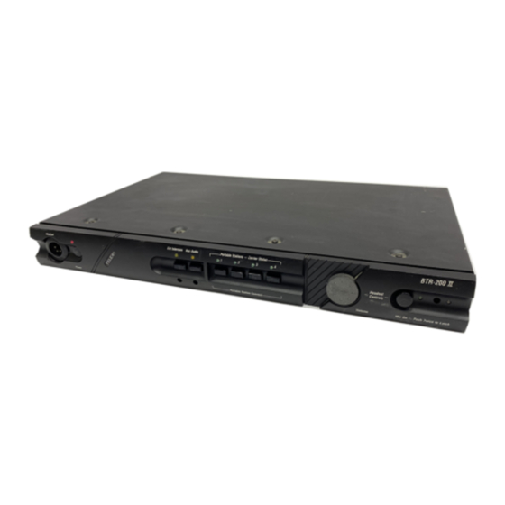
POWER ON INDICATOR Headset . LOCAL HEADSET CONNECTOR INTERCOM ENABLE SWITCH INTERCOM INDICATOR AUXILIARY ENABLE INDICATOR PORTABLE CARRIER INDICATORS I.-.--~ Portabte Station Connect-- ENABLE SWITCHES TO RECEIVE PORTABLE TRANSMITTERS AUXILIARY LEVEL CONTROL AUXILIARY ENABLE SWITCH INTERCOM LEVEL CONTROL Figure 2 Front Panel-BTR200 27160-8-00I-A ~OCAL... -
Page 7: Rear Panel - Btr-200
Input Transmit Cant Off Remote TRANSMITTER SWITCH SPEAKER / LOCAL MONITOR (8 Figure 3 Rear Panel BTR-200 27160-B-002-A RECEIVE ANTENNA CONNECTOR TELEX COMMUNICA TtONS. INC. Fex 1.0. 850BTR-200 MADE IN U.S.A. Power A~'~ Jack LSpeaker-l ------- 300 rnA POWER JACK SPEAKER GAIN CONTROL MIN.) -
Page 8: Rear Panel
Electret or Dynamic microphone. This switch to DYN Position. NOTE: All Telex headsets that are used with this intercom are dynamic type microphones. Auxiliary Audio Enable Switch, Level Control, and Indicator: The switch enables and disables the Auxiliary intelface when "IN"... -
Page 9: Chapter 2 - Identification Of Circuit Board Revision And Version
IDENTIFICATION OF CIRCUIT BOARD Version 1 and 2 use Rev A circuit boards. The location for the Rev letter is shown below. Version 2 contains a small circuit board with a switch. See Figure 4. CHAPTER 2 REVISION AND VERSION AUDIO BOARDS This board is installed in the holes for C124 and C125 (see below). -
Page 10: Receive Board
Rev C boards can be either Verion 3 or 4. The differences are all parts values: Version RIOI RI03 Rl25 6.2K 200K 200K 4.7K The BTR-200 uses one of two receive boards. Early production units came with 70714000, and 750309 was installed in later units. came in two versions that differed slightly (See table below): Version 2 was built only with Rev C boards. - Page 11 TRANSMIT BOARD ,.-- -------- 7-------- '70"12' ..-000 70724-000 REV A COMP Figure 7 Location of Rev Level for Versions 1 and 2 All Rev A boards are version Rev B boards may be version 1 or 2: Version R503 R521 CS31 4.7K...
-
Page 12: Exploded View - Btr-200
878520 PCB, Audio 878517 Connector bracket 51847011 Screw, #4-40 x 1/4", flathead 59908001 Connector, B4MB Switchcraft 878560 Wireset 150624-3 Telex label 52264005 Connector Housing, 5 Pin 878439-3 Front Panel 0086300 Copper strip, .343 x .005 878430 Chassis 878521 Transmit Board... - Page 13 TRANSMIT, RECEIVE & AUDIO CIRCUIT,BOARDS BTR-200 INSTRUMENT DISASSEMBLY 1. Remove 6 each #6 pan head phillips and #14 head phillips screws and remove cover. Refer to Figure 8. 2. Unsolder coax cables from transmit and receive boards. 3. Unsolder 3 copper straps from receive board (if present) 4.
-
Page 14: Transmit Board
CIRCUIT DESCRIPTION U50IC is an amplifier whose gain is controlled by the level of audio entering the rectifier at pin 16. As the level here increases, the gain is decreased and this results in a 2:1 compression characteristic. Pre-emphasis is added by U501B. R504, R505, and C508 set this at 115uS. -
Page 15: Voltage Tables - Transmit Board (878521)
Voltage Tables - Transmit Board (878521) 1====-r===r===r====jPI=N=N=U=rM=B=E"F'R==~===r==~==l1 DEVICE U501 DEVICE Q50l 1.88 Q502 0.78 Q503 1.21 PIN NUMBER 2.44 0.66 0.26 .--- U501 Q501, Q502 ---, Q503... - Page 16 Transmit Board Component Layout (Foil Side) C501 USO 1 +~04 R502 -e::>- ~nc5°bc50~ ",y 1505 CS08 -e:::>- c:::> -e::>- R501 R504 C507 C5<t9,.-t VRS01 Transmit Board Component Layout (Component Side) Figure 9 C503 PS12 l'lN OC506 U502 CS11 I()C512QQ nS005&' 05'3-/\10 I 0 I I 0 I...
- Page 17 G511 10UF G509 4.7UF C510 4-.7UF t-+-'-~\I\1~-' VR501 C513 100pf 47K R502 R501 C506 loopf 20 12 G50J R521 P512 I .. C505 4-.7UF G501 .. C504- lOoU~ R508 WC501 MV21 08 R507 FREQUENCY DEPENDENT COMPONENTS TABLE T501 FREQUENCY C516 C519 C520 C523...
- Page 18 R502 R501 C506 100P~ "'f 20 12 P512 j'" 16--l 3.9K C505 4.7UF C501 .. C504 100U1 j" j'" U502 78L05 C511i 10U~ j'" FREQUENCY DE:PENDENT COMPONENTS TABLE T501 FREQUENCY C516 C519 C520 C523 C524 C529 C5JO T501 154.570 MHZ 27PF 39PF 100PF 18PF 33PF 68PF 20PF -000 177.800 MHZ 22PF 30PF 75PF 12PF 27PF 47PF 15PF -002 183.730 MHZ 22PF 30PF 75PF 12PF 24PF 47PF 15PF -002 Figure 12...
- Page 19 PCB Transmit Assembly (878521-*) Ref No. Description PCB500 PCB Transmit Capacitors All capacitors in microfarads unless noted. Ref No. Description C501 Electrolytic, 100 C502-C504 Electrolytic, 1 C505 Electrolytic, 4.7 Ceramic, 100 pF C506 C507 Electrolytic, 1 C508 Film, poly, .01 C509-C51O Electrolytic, 4.7 C511...
-
Page 20: Receive Board
CIRCUIT DESCRIPTION PCB 70714000 This unit is a four channel single conversion receiver consisting of one front end and four I.F. strips. Signals entering the board proceed through 3 tuned circuits, Q30l, and 3 more tuned circuits to the mixer. MX301 is a doubly balanced diode mixer and receives +7 dBm from the oscillator. -
Page 21: Alignment Procedure
ALIGNMENT PROCEDURE Equipment Required: Signal Generator Sensitive RF Voltmeter DC Voltmeter AF Voltmeter 1. Connect the signal generator to the Receive Antenna jack. Set the deviation at 1 KHz. Refer to the frequency chart below. Look at the marking on the Y301 and set the generator to the corresponding ALIGN fre- quency. -
Page 22: Receive Board (750309)
23. Adjust T31O, T311, T312, T313, and T314 for maximum DC voltage at pin 5 of U304. 24. Set the signal generator output to 1 mV and adjust T315 for maximum audio at pin 7 of U305. 25. Adjust VR304 for 140 mV of audio at pin 7 of U305. - Page 23 4. Connect the signal generator to the Receive Antenna jack. Set the deviation to I KHz. Refer to the chart and select the channel 3 frequency. 5. Connect the AF voltmeter, distortion meter, and SINAD meter to U421 pin 1. Adjust VR421 to maximum counterclockwise.
- Page 24 NOTES: 3-13...
-
Page 25: Voltage Tables - Receive Board (70714000)
Voltage Tables - Receive Board (70714000) Q301 DEVICE Q302 2.54 Q303 Q304, Q306, 2.63 Q308, Q310 Q305, Q307, Q309, Q311 6.65 7.34 DEVICE t==r-=r-=PrIN=N=UrM=B=E=Rr===r====r=====I U301 1.58 1.58 1.61 U304 U306 U309 PIN NUMBER DEVICE 1I==,=====,====P U301 1.58 1.58 1.61 U304 U306 U309 1.58... -
Page 26: Voltage Tables - Receive Board (750309)
Voltage Tables· Receive Board (70714000) Continued DEVICE ..._PIN.,.-N_U"T"M_B..,.E_R-==J DEVICE t===P.,..IN=N_U=M=B...,E.-=R==j 8 7 6 10 0.05 U303 U305 U302 U307 U308 U310 5 5 0 0.05 2 3 4 1 2 3 PIN NUMBER PIN NUMBER Voltage Tables - Receive Board (750309) L303 DEVICE VERSION Gl G2 NOTE: If this part is... - Page 27 ~------------------------jr------------r------------------,-----j f-f:" C31J CJOl CaD;:} CJ05 Q301 3SK174 VCJO~ ()--j i-------, VCJOJ*r;;..::=.-_-+,,,,,b'-1 VC,JOl "l LJ05 C 3 0 : : f LJ02 VC305, VC30. LJOl CJoa lOOPF FL305 , FREQUENCY FL306 C3921 C393 IC3941c3951c3961c3971c3981c3991 C400 1 C405 IC4061c4071 C408 IC4121 '169 172 MHZ 12.36MHZ 43PF 330PF 168PF 150PF 1.82PFI36PF!.82PFI43PF 1330PF...
- Page 28 SHL~ @c::::J@FU03 ~ANT::::;/~g ° <>1 1301r N~§1J0303 T311Fo~CJeO ~~~~~&>C359 ro~o~~j~~~ @(f10R312@ 0 CO>c325C360Cjg 0 VC301 @o:: <O>c324 C304CCb @@C303 @ @-U09-@ vn020=:<\"y'::\ lf1C3oitQ> C323 0 l~gAC326JO 0 00_ 1302 L.302 L303 T30310 I @ _ If(§) ?o 0 ° . VCJ03 @R301@ ~302@...
- Page 29 P301 R305 R306 C301 C302 C306 o--1~~VC303 C30~ L302 VC305 VC306 L301 C305 lOOP/, R307 2.2K C422 ,C472 CF370 CF420 CF470 FREQUENCY C301 C302 C303 C307 C308 C313 C421 CF371 CF421 CF471 11.56 12.36 13,1 pI' 1.2pF 4.7 pI' pI' 43 PI' 39pF 169-172 pI' 43 pI' 11.075...
- Page 30 r:--------, > 3-19 Figure 1'"( Receive Board Componen~ Layout (Foil Side) vo~oQ01oI~~o~ 1000I~':CD~'t -c:>- C305 L304 • -e> c=:Jo C30l C302 C303 R30l R303 C3150 -e> R313 FB371 OR321 FB321 Q37b R37l Q320 R380 R330 -e> <:> L373 R470 <:> -e>...
- Page 31 PJ01 R306 "0 CJ', C318 CJ<lB R305 100PF I·oo1uF I,001uF RJ15 C301 1'" 1'" C"2 C3" CJ<l~V"OB "'05 I.305 ",307 3.JK FREQUENCY DEPENDENT COMPONENTS TABLE CF370 CF420 CF470 FREQUENCY CJ01 C302 C30J C307 CJOB CJ1J C421 C422 C472 L306 Y301 Y370 Y420 Y470...
- Page 32 Description Ref No. PCB300/400 Printed Circuit Board, Receive Capacitors All capacitors in microfarads unless noted. Description Ref No. C301 Ceramic, 5.6 pF 2 ,3 C301 Ceramic, 4.7 pF C302 (Not Used) C303 Ceramic, .82 pF 2 ,3 C303 Ceramic, .5 pF C304 (Not Used) C305...
- Page 33 PCB Receive Assembly 878522-* (Continued) Description RerNo. C406 Ceramic, 20 pF 2 ,3 C406 Ceramic, 24 pF Ceramic, 20 pF C407 2 ,3 C407 Ceramic, 24 pF Ceramic, 330 pF C408 2 ,3 C408 Ceramic, 270 pF Ceramic, .01 C409, C410 Ceramic, 2.2 pF C411 Ceramic, 36 pF...
- Page 34 Ref No. Description Crystals and Filters Crystal Filter Insulator MX301 Mixer, ASK-1 Y301' Crystal, Receive, 171.905 MHz Crystal, Receive, 207.800 MHz Y301 Y301 Crystal, Receive, 213.800 MHz Filter, 10.7 Crystal FL301 FL302 Filter, 11.56 MHz Crystal FL303 2 ,3 FL303 Filter, 11.075 MHz Crystal FL304' Filter, 11.56 MHz Cryst31...
- Page 35 PCB Receive Assembly 878662-* Description Ref No. Printed Circuit Board, Receive Capacitors All capacitors in microfarads unless noted. Ref No. Description C301 Ceramic, 5.6 pF 2 ,3 C301 Ceramic, 4.7 pF C302 Ceramic, .82 pF 2 ,3 C302 Ceramic, C303 Ceramic, 2 ,3 C303...
- Page 36 Description Ref No. Potentiometers 20K Potentiometer VR320 50K Potentiometer VR321 20K Potentiometer VR370 50K Potentiometer VR371 VR420 20K potentiometer VR421 50K Potentiometer VR470 20K Potentiometer 50K Potentiometer VR321 Colls and Chokes L301,L302 Coil, 2 1I2T, 10 mm . L303,L304 Coil, 2 1/2 CT, 10 mm Coil, 2 1I2T, 10 mm L305 Coil,2 1I4T, 114 Tap, 10 mm...
- Page 37 PCB Receive Assembly 878662-* (Continued) Resistors (Continued) Ref No. Description R327 lOOK R328 R329, R330 220K R331 R332-R334 (Not Used) R335-R369 R370 1.2K R371 R372 R373 l.5K R374 R375 330K R376 220K R377 lOOK R378 R379, R380 220K R381 R382-R384 R385-R419 (Not Used) R420...
-
Page 38: Audio Board
DIP switch which is used to configure the base for compatability with a specific wired inter- com. S103 functions as either an intercom onloff switch.(Telex, Clearcom standard) or as a channel AlB switch (RTS, Clem'com TW). In the case where the intercom interface is disconnected by S 103, R 186 functions as the load resistor. -
Page 39: Intercom Input
On versions 3 and later, U118 acts as a four pole Chebyshev low pass filter with a cutoff frequency of 5 KHz. This is to prevent transmis- sion of the 20 KHz tone which Telex intercoms use as the call signal. Auxiliary Output UllOA mixes together intercom input, microphone, and receive board signals. -
Page 40: Alignment Procedure
ALIGNMENT PROCEDURE: Equipment Required: Signal Generator Audio Generator Deviation Meter Audio Voltmeter Connect the audio generator to the AUX IN jack and set the output to 20 mV at 1 2. Select the AUX pushbutton on therront panel. Adjust VR601 (located just under the I1C push- button on the front panel) to maximum counterclockwise. - Page 41 RECEIVER 1 EXPANDER RECEIVER 2 EXPANDER RECEIVER 3 EXPANDER RECEIVER 4 EXPANDER DYNAMIC/ ELECTRET _~~ ... HEADSET I.4ICROPHONE AUXIN 3-31 __---------, I--"~ __--"" I---"~ I---"~ - - - - - - + I (ON VERSION 2 ONLy) IC---...~ - . J MIC GAIN Figure 19 Block Diagram Versions 1 and 2...
- Page 42 ---1 . . - ------- I--"~ RECEIVER 1 EXPANDER ---1 RECEIVER EXPANDER ---1 ~_------toI RECENER EXPANDER ---1 I--"'~--"'/ RECEIVER 4 EXPANDER DYNAMIC/ ELECTRET HEADSET MICROPHONE AUX GAIN AUX IN Block Diagram Versions 3 thru 6 INTERCOM GAIN BALANCE HIGH/LOW Figure 20 AUX OUT TRANSMIT OUT INTERCOM...
- Page 43 C144 C145 FIGURE Ul08 (aanaaaaaaal DETAIL R1840 s O O O Q 1 8 1 C143 C142 c:::J O O R l 8 2 Cl48 C148 SlO9 3-33 Jl04 J10S <:) C1S8 C1S9 C181 +0 0+ C17~ C188 C164 0 Co C1800"': : ...
- Page 44 Figure 22 Audio Board Component Layout (Foil Side) Versions 1 and 2 3-34...
-
Page 45: Display Board
el03 .0022UF 0110 lN4148 ~01J r.-r ~~R-2~'2-----'8 ~~~g:B Dl09 , r-:l lN4146 11'OOK Q'f~'+--1~-+-"".I'--!I--~ S110 : ~ ' ~ : : : i ' ~~C TAlK JOOK lo--------l<I D!,0~8 R213 -:::" C184- __j-----1T~TI---v'VDKIr1'__j r-_ _ . It R217 R214 R216 R211 c,'~iI lOOK... - Page 46 U " ' : A " 1,C'63 1° NE575 10QPF PORTABLE 1 9!~~~OK I . , .. 0 SELECT 'o,V F ,:...J U112'8 0111 ~>-----------------\-----. ~75. S~ 10I'U'_'v6B'vK,-_~ Jl09 3.•K lOU' Rl~5J7 ~ 1~JgJ' 1,RJ;~~~~f PORTABLE C'6': ~ 0~~:"702 06051 lU'I ~~;~ u~~~~~...
- Page 47 NOTE: VERSION 1 DOES NOT HAVE THE SWITCH BOARD ASSEMBLY. C124 AND C125 WILL BE LOCATED ON THE AUDIO BOARD RATHER THAN ON THE SWITCH BOARD. ----.lI~-.=Joqa '~.C_ ·@5 Riv.A Figure 25 Details of Board Differences Between Versions 1 and 2 3-37...
- Page 48 Q105"-../ R185 oc::::Jo DR222 U115 C144 C145 U108(;)(;) laaaa aaa aaaa 0 070'\0 R184~~~~l8 d)(;) R182 C148 C146 Details of Board Difference in Versions 3, 4, 5, and 6 QC117 R134D C136 P103 Detail A C141 R181 C142 Detail B Figure 26 3-38 NOTE: THIS AREA OF THE...
- Page 49 01llS""""'" 1117 R:l112 Dl117 '---J ~& gggg '"'' 2:i'Q.. ''''. . U117 R2ll9 R2Il8 c::::J '" ... '" ~ ~ ~ <II 3-39 JlllS VRlllJ Jlll4 Jl00 C157 Cl:l8 O2113 Cl5!1 +0 + C1Ii6 CJ.Z! u· Cl800+ C162 +~ D~ Pcg;...
- Page 50 ". NOTE: REFER TO FIGURES 26 Figure 28 AND 27 FOR DIFFERENCES IN Audio Board Component Layout (Foil Side) VERSIONS 3, 4, AND 5. Version 6 3-40...
- Page 51 U112:A NE575 I" C159~0J( ioil;' • \--.>---R-,9-5-------------t----.,IH 3.9Kr L, r« JlOO: 1 IK C;~9 • +1·our=I PORTABLE I' CI64 , 1 -,'06051 MPS3702 I :; I u~~~~~ R2'O 0100 3.3K C I 6 0 t t : 3 : ' ' - I ' O I U ~ . . . j F '-==:.:' --l-_--l- =-=_:...I--+...
- Page 52 U"2:A J,C163 100Pf NE575 PORTAI3LE 1 C159¢:;OK SELECT ,<iii ::.J; U112:8 C171 C'72 R'30 >-----------------l---:.;"IJ:--l, llil t;:-- NE575. ',OUF S1..9i fi±----' v V' - ---., ~ R~~~ J109 r-v--- IR'~~rR'96 '----+---r.,..-,-J '1 I , +~M~=f C165 lOOKl'OOK ~L~4 +1_ 0605 PORTABLE 1 MPS3702 ..hiOOUF...
- Page 53 U1120A J,CI6J 'OOPF NE575 PORTABLE 1 r' " C159~OK I , . . . SELECT C172 iO~F I, I ~l1~g fJJ~ ,::J; '---R-"19-"5--;;;01~"'2;;-------+----:;.~H ~"""j~ 1~,,,U~,F-,,4,,,.7/,-K_~ 5105 ,>- 3,9K Jl09, IIPS370 '---1---,r;---,-' R194 R198 • cj~!~ R210 lOOK lOOK 't"OUFT 3.3K C185 PORTABLE l' C164 +...
- Page 54 U112:A ±C163 NE575 100PF PORTABLE 1 C159~OK... r..::::. SELECT 10~F U'12:B C171 C172 R130 r-,>--::Rl:-:~:-5-M-PS3---;;~;-;I;;;;~2--------I-----':.l+ 3.9K8~ ~S.2h~I'U~F--'lJ4.,,7K,-_-, J,09 *rJe~~ ~ ~~~~ '00K ~L~4 C165 100Kl 00051 !-'N--g\!), PORTABLE 1 MPS3702 lOOUF Ql09 U112:C NE575 PORTABLE 2 10UF~ I" U112:0 C173 SELECT C174 r-,-R-,1-K96-M=PS3=-=:~=6Y7\C:3=--H----if-------...ijHi..l I"...
- Page 55 PCB Audio Assembly, (878520) Versions 1 thru 6 Ref No. Description Printed Circuit Board, Audio IPCB100nOO Capacitors in microfarads unless noted. AU capacitors Description Ref No. Electrolytic, 2.2 C101, C102 CI03 Poly film, .0022 CI04 Ceramic, 100 pF Electrolytic, 1 CI05 C106 Ceramic, .01...
- Page 56 PCB Audio Assembly (878520) Versions 1 thru 6 Continued Description Ref No. Connectors 1101 Connector, 3 Pin, XLR Female 1102 (Not Used) 1103 Connector, 3 Pin, XLR Male 1104 Connector,3 Pin, XLR Female 1105 Connector, 3 Pin, XLR Male 1106 Jack, speaker, 1/4"...
- Page 57 Audio Assembly (878520) Versions 1 thru 6 Continued All resistors in ohms, 1/8 watt, 5 % unless noted. Resistors & Potentiometers Continued Ref No. Description Part No. R182 1,1/4 watt 52154909 1 - 5 R183 52154030 R183 (Not Used) R184 52154077 R185 3.6K...
- Page 58 PCB Display (878519) Ref No. Description Part No. J601 Cable Assembly 640063-3 J602 Cable Assembly 640063-3 Sprocket 450464 VR601 Pilier Potentiometel~ lOOK 724779 VR602 Piber Potentiometer, lOOK 724779 VR603 Volumne Potentiometer 723087 VR604 Piber Potentiometer, lOOK 724779 PCB600 PCB, Display 70716000 LED601 LED,Red...
- Page 59 _ _ _ _ _ _TELEX@ Printed in U.S.A. PN 802482 24 MAR 1993...