Sony GV-D200 Service Manual
Digital video cassette recorder
Hide thumbs
Also See for GV-D200:
- Operating instructions manual (76 pages) ,
- Specifications (2 pages) ,
- Service manual (81 pages)
Table of Contents
Advertisement
GV-D200/D200E/D800/D800E
SERVICE MANUAL
Ver 1.2 2003. 06
NTSC MODEL : GV-D200/D800
PAL MODEL
: GV-D200E/D800E
Function difference table
Model
GV-D200/200E
Function
LCD
—
VCR
System
Video recording system
2 rotary heads
Helical scanning system
Audio recording system
Rotary heads, PCM system
Quantization: 12 bits (Fs 32 kHz,
stereo 1, stereo 2), 16 bits (Fs 48 kHz,
stereo)
Video signal
GV-D200/D800:
NTSC color, EIA standards
GV-D200E/D800E:
PAL colour, CCIR standards
Recommended cassette
Hi8
/Digital8
video cassette
Recording/playback time
(GV-D200/D800: using
120 min. Hi8 video cassette)
(GV-D200E/D800E: using
90 min. Hi8 (PAL) video cassette)
SP mode: 1 hour
LP mode: 1 hour and 30 minutes
Fastforward/rewind time
(GV-D200/D800: using
120 min. Hi8 video cassette)
(GV-D200E/D800E: using
90 min. Hi8 (PAL) video cassette)
Approx. 5 minutes and 15 seconds
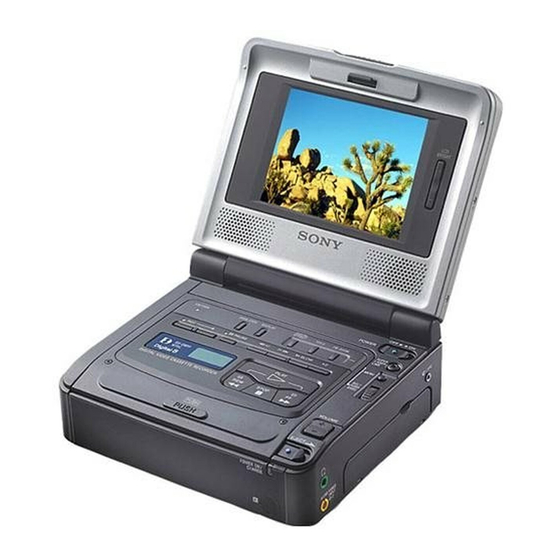
Photo : GV-D800E
GV-D800/D800E
4.0 inches
SPECIFICATIONS
Input/output
connectors
S video input
4-pin mini DIN
Luminance signal: 1 Vp-p, 75 ohms,
unbalanced
GV-D200/D800:
Chrominance signal: 0.286 Vp-p
GV-D200E/D800E:
Chrominance signal: 0.3 Vp-p,
75 ohms, unbalanced
S video output
4-pin mini DIN
Luminance signal: 1 Vp-p, 75 ohms,
unbalanced
GV-D200/D800:
Chrominance signal: 0.286 Vp-p
GV-D200E/D800E:
Chrominance signal: 0.3 Vp-p,
75 ohms, unbalanced
Audio/Video input
AV MINIJACK
Video: 1 Vp-p, 75 ohms, unbalanced,
sync negative
Audio: 327 mV, input impedance
more than 47 kiloohms
Video output
Phono jack, 1 Vp-p, 75 ohms,
unbalanced, sync negative
Audio output
Phono jacks (2) 327 mV, output
impedance less than 1 kiloohm
RFU DC OUT
Special minijack DC 5 V
DIGITAL VIDEO CASSETTE RECORDER
For MECHANISM ADJUSTMENT, refer to
the "8mm Video MECHANICAL
ADJUSTMENT MANUAL
DV input/output
4-pin connector
Headphone jack
Stereo minijack (ø 3.5 mm)
LANC
jack
Stereo mini-minijack (ø 2.5 mm)
LCD screen (GV-D800/D800E)
Picture
4.0 type
80.6 × 60.5 mm (3 1/4 × 2 1/2 in.)
Total dot number
123,200 (560 × 220)
General
Power requirements
7.2 V (battery pack)
8.4 V (AC power adaptor)
Average power consumption
(when using the battery pack)
GV-D800/D800E only
During playback using LCD
4.9 W
During playing back when you close
the LCD panel
3.0 W
Operating temperature
0 °C to 40 °C (32 °F to 104 °F)
Storage temperature
–20 °C to +60 °C (–4 °F to +140 °F)
US Model
Canadian Model
GV-D200/D800
AEP Model
UK Model
E Model
GV-D200E/D800E
B MECHANISM
" (9-973-801-11).
Dimensions (Approx.)
GV-D200/D200E:
148 × 50 × 135 mm
(5 7/8 × 2 × 5 3/8 in.)
GV-D800/D800E:
148 × 65 × 135 mm
(5 7/8 × 2 5/8 × 5 3/8 in.) (w/h/d)
Mass (approx.)
GV-D200/D200E:
660 g (1 lb 7 oz)
GV-D800/D800E:
930 g (2 lb)
excluding the battery pack and
cassette
Supplied accessories
See page 2.
AC power adaptor
Power requirements
100 - 240 V AC, 50/60 Hz
Power consumption
23 W
Output voltage
DC OUT: 8.4 V, 1.5 A in the
operating mode
Operating temperature
0 °C to 40 °C (32 °F to 104 °F)
Storage temperature
–20 °C to +60 °C (–4 °F to +140 °F)
— Continued on next page —
Advertisement
Table of Contents

Related Manuals for Sony GV-D200


Summary of Contents for Sony GV-D200
- Page 1 AEP Model Ver 1.2 2003. 06 UK Model E Model GV-D200E/D800E B MECHANISM Photo : GV-D800E NTSC MODEL : GV-D200/D800 For MECHANISM ADJUSTMENT, refer to PAL MODEL : GV-D200E/D800E the “8mm Video MECHANICAL Function difference table ADJUSTMENT MANUAL ” (9-973-801-11).
-
Page 2: Supplied Accessories
MARK 0 ON THE SCHEMATIC DIAGRAMS AND IN THE PARTS CRITIQUES POUR LA SÉCURITÉ DE FONCTIONNEMENT. NE LIST ARE CRITICAL TO SAFE OPERATION. REPLACE THESE REMPLACER CES COMPOSANTS QUE PAR DES PIÈSES SONY COMPONENTS WITH SONY PARTS WHOSE PART NUMBERS DONT LES NUMÉROS SONT DONNÉS DANS CE MANUEL OU APPEAR AS SHOWN IN THIS MANUAL OR IN SUPPLEMENTS DANS LES SUPPÉMENTS PUBLIÉS PAR SONY. -
Page 3: Table Of Contents
TABLE OF CONTENTS SERVICE NOTE 2-4. PD-130, LS-56 BOARDS (D800, D800E MODEL) ······ 2-4 2-5. LCD WINDOW CABINET ASSEMBLY (SP-901, 902) POWER SUPPLY DURING REPAIRS ····························· 6 (D800, D800E MODEL) ················································· 2-5 TO TAKE OUT A CASSETTE WHEN NOT EJECT 2-6. - Page 4 • VC-250 (DC/DC CONVERTER)(15/16) 8 Page Table ··································································· 5-13 SCHEMATIC DIAGRAM ···························· 4-39 3-2-2. INITIALIZATION OF E, F, 7 PAGE DATA ················· 5-14 • VC-250 (CONNECTION)(16/16) Initializing the E, F, 7 Page Data ··································· 5-14 SCHEMATIC DIAGRAM ···························· 4-41 Modification of E, F, 7 Page Data ································· 5-14 •...
- Page 5 2-1. C Page Emergence Memory Address ···························· 5-41 2-2. F Page Emergence Memory Address ···························· 5-42 2-3. EMG Code (Emergency Code) ····································· 5-42 2-4. MSW Code ···································································· 5-43 Bit Value Discrimination ··············································· 5-44 Switch check (1) ···························································· 5-44 Switch check (2) ···························································· 5-44 Switch check (3) ····························································...
-
Page 6: Service Note
SERVICE NOTE POWER SUPPLY DURING REPAIRS In this unit, about 10 seconds after power is supplied (8.4V) to the battery terminal using the service power code (J-6082-223-A), the power is shut off so that the unit cannot operate. These following two methods are available to prevent this. Take note of which to use during repairs. Method 1: Connect the adjustment remote commander RM-95 (J-6082-053-B) to the LANC jack, and set the HOLD switch to the “ADJ”... -
Page 7: To Take Out A Cassette When Not Eject (Force Eject) (2
TO TAKE OUT A CASSETTE WHEN NOT EJECT (FORCE EJECT) (2) (TO TAKE OUT A CASSETTE WITHOUT HURTING THE TAPE) 1 Disconnect the power supply (Battery or AC adaptor) 2 Refer to 2-2. to remove the cabinet (lid) assembly. 3 Refer to 2-2. to remove the cabinet (bottom) assembly. 4 Refer to 2-1. -
Page 8: Self-Diagnosis Function
SELF-DIAGNOSIS FUNCTION SELF-DIAGNOSIS FUNCTION SELF-DIAGNOSIS DISPLAY When problems occur while the unit is operating, the counter of the When problems occur while the unit is operating, the self-diagnosis function starts working, and displays on the LCD screen or monitor viewfinder shows a 4-digit display consisting of an alphabet and TV (Note) what to do. -
Page 9: Self-Diagnosis Code Table
SELF-DIAGNOSIS CODE TABLE Self-diagnosis Code Block Detailed Symptom/State Correction Function Code Non-standard battery is used. Use the info LITHIUM battery. Condensation. Remove the cassette, and insert it again after one hour. Video head is dirty. Clean with the optional cleaning cassette. LOAD direction. -
Page 10: General
GV-D200/D200E/D800/D800E SECTION 1 This section is extracted from instruction GENERAL manual. (GV-D800E model) - Page 19 1-10...
- Page 20 1-11...
- Page 21 1-12...
- Page 22 1-13...
- Page 23 1-14...
- Page 24 1-15...
- Page 25 1-16...
- Page 26 1-17...
- Page 27 1-18...
- Page 28 1-19...
- Page 29 1-20...
- Page 30 1-21...
- Page 31 1-22...
- Page 32 1-23E...
-
Page 33: Disassembly
GV-D200/D200E/D800/D800E SECTION 2 DISASSEMBLY The following flow chart shows the disassembly procedure. 2-1. Cassette Lid assembly 2-2. Bottom cabinet assembly, FP-571 flexible board (Lithium battery) PD-130 board service position 2-3. LCD cabinet assembly (D800, D800E model) (D800, D800E model) 2-6. Battery panel assembly, Battery terminal board, 2-4. -
Page 34: Cassette Lid Assembly
NOTE: Follow the disassembly procedure in the numerical order given. 2-1. CASSETTE LID ASSEMBLY 2 Two screws (M2 × 4), lock ace, p2 1 Open the LCD panel in the direction of the arrow A . 6 Cassette lid (GV-D800/D800E model) assembly Push 5 Claw... -
Page 35: Board (Lithium Battery)
2-3. LCD CABINET ASSEMBLY (D800, D800E MODEL) 2 Two screws (M2 × 4), lock ace, p2 6 Remove the LCD cabinet assembly in the direction of the arrow. 3 Two screws (M2 × 3), lock ace, p2 1 Two screws (M2 × 4), lock ace, p2 4 Two claws... -
Page 36: Boards (D800, D800E Model)
2-4. PD-130, LS-56 BOARDS (D800, D800E MODEL) 9 Three screws (M2 × 3), lock ace, p2 6 Two tapping screws (B2 × 5) 0 Remove the PD-130 board 7 FP-569 flexible in the direction of the arrow. board (26, 32P) 3 Harness (PL-53) (2P) 8 Harness (EP-51) (2P) qs LS-56 board, LS bracket... -
Page 37: Lcd Window Cabinet Assembly (Sp-901, 902)
2-5. LCD WINDOW CABINET ASSEMBLY (SP-901, 902)(D800, D800E MODEL) 1 Two tapping screws (B2 × 5) 2 Two tapping screws (B2 × 5) 5 LCD ground plate 3 PD frame 4 Screw (M2 × 3), lock ace, p2 6 LCD901 9 ND901 7 Two claws 8 Two claws... -
Page 38: Battery Panel Assembly, Battery Terminal
2-6. BATTERY PANEL ASSEMBLY, BATTERY TERMINAL BOARD, DC-IN CONNECTOR 7 Two tapping screws (B2 × 5) 0 Mechanism section 9 DC-IN connector (3P), DC jack assembly 6 Battery panel assembly, Battery terminal board 5 FP-247 flexible board (50P) 3 FP-569 flexible board (26, 32P) 1 FP-570 flexible board (40P) -
Page 39: Control Switch Block (Fk-78), Loading Lid
2-8. CONTROL SWITCH BLOCK (FK-78), LOADING LID 2 Screw (M1.4 × 1.6) 1 Remove the control switch block (FK-78) (10P) in the direction of the arrow. 6 Control switch block (FK-78) (10P) 7 Two screws (M2 × 4), lock ace, p2 3 Screw (M1.4 ×... -
Page 40: Cabinet (R) Block Assembly, Jack Frame
2-10. CABINET (R) BLOCK ASSEMBLY, JACK FRAME (IO-68, IR-38 BOARDS) 2 Cabinet (R) block assembly 1 Three tapping screws (B2 × 5) 3 Five tapping screws (B2 × 6) 4 Cabinet (R) REMOVING THE JACK FRAME 8 Screw (M2 × 3), 5 FP-247 flexible lock ace, p2 board (50P) -
Page 41: Upper Cabinet Assembly
2-11.EX-36 BOARD, FP-570 FLEXIBLE BOARD 1 Three tapping screws (B2 × 5) 2 Harness (EP-51) (2P) 3 EX-36 board, FP-570 flexible board (40P) 2-12.UPPER CABINET ASSEMBLY, LCD BLOCK ASSEMBLY (D800, D800E MODEL) 2 FP-602 flexible board (5P), Strap sheet metal (L) 4 Strap sheet metal (R) 5 Upper cabinet assembly 3 Two screws (M2 ×... - Page 42 2-13.HINGE UNIT, FP-569 FLEXIBLE BOARD (D800, D800E MODEL) When attaching the hinge unit, wrap the FP-569 flexible board hinge shaft as shown while taking care so that the flexible board must not be caught or pinched. Hinge unit FP-569 flexible board (26, 32P) 3 FP-569 flexible board (26, 32P)
- Page 43 [CONNECTION DIAGRAM FOR SERVICE POSITION (Mainly for voltage measurement and check)] (VC-250, FU-145, IO-68 BOARDS, MECHANISM DECK) Control switch block (FK-78) (10P) CPC-13 jig (J-6082-443-A) VC-250 board CN933 AC POWER ADAPTOR AC IN DC-IN connector (3P), DC jack assembly Battery panel assembly, Battery terminal board FP-247 flexible board (50P)
-
Page 44: Circuit Boards Location
2-14.CIRCUIT BOARDS LOCATION LCD DISPLAY MODULE (D800/D800E ONLY) PD-130 LCD DRIVER, FP-602 BACK LIGHT (DV IN/OUT) LS-56 (LCD SWITCH) EX-36 (MULTI CONNECTOR) IR-38 (IR TRANSMITTER) FP-575 (LANC) FU-145 (DC/DC CONVERTER) IO-68 (AV IN/OUT) FP-246 (REMOTE COMMANDER RECEIVER) VC-250 REC/PB AMP, DAC, DV INTERFACE, AD CONVERTER, Y/C PROCESSOR, LINE A/D, LINE IN/OUT, IR, AUDIO IN/OUT, DRUM/CAPSTAN MOTOR DRIVE, MECHA CONTROL, HI CONTROL, DC/DC CONVERTER 2-12... -
Page 45: Flexible Boards Location
2-15.FLEXIBLE BOARDS LOCATION The flexible boards contained in the mechanism deck are not shown. CONTROL SWITCH BLOCK (FK-78) FP-570 FP-571 FP-569 FP-572 FP-247 2-13E... -
Page 46: Block Diagrams
GV-D200/D200E/D800/D800E SECTION 3 BLOCK DIAGRAMS 3-1. OVERALL BLOCK DIAGRAM (1/4) ( ) : Page No. shown in ( ) indicates the page to refer on the schematic diagram. (SEE PAGE 4-45) IO-68 BOARD VC-250 BOARD(1/4) (4-26) (4-23) (1/2) (4-25) IC3701... -
Page 47: Overall Block Diagram (2/4)
GV-D200/D200E/D800/D800E 3-2. OVERALL BLOCK DIAGRAM (2/4) ( ) : Page No. shown in ( ) indicates the page to refer on the schematic diagram. CN1105 VC-250 BOARD(2/4) DV IN/OUT (4-15) X3301 IC3301 24.576MHz (CAIN) CN929 CN1104 (4-17) TPA+,- DV SIGNAL... -
Page 48: Overall Block Diagram (3/4)
GV-D200/D200E/D800/D800E 3-3. OVERALL BLOCK DIAGRAM (3/4) ( ) : Page No. shown in ( ) indicates the page to refer on the schematic diagram. B710-MECHA DECK FU-145 BOARD(1/2) VC-250 BOARD(3/4) (4-33) (SEE PAGE 4-56) (4-35) (4-33) CN921 M901 IC4401 IC1301... -
Page 49: Overall Block Diagram (4/4)
GV-D200/D200E/D800/D800E 3-4. OVERALL BLOCK DIAGRAM (4/4) ( ) : Page No. shown in ( ) indicates the page to refer on the schematic diagram. (GV-D800/D800E) PD-130 LS-56 BOARD FK-78 BOARD VC-250 BOARD (4/4) (4-37) BOARD (3/3) IC4803 (SEE PAGE 4-61) -
Page 50: Power Block Diagram (1/2)
GV-D200/D200E/D800/D800E 3-5. POWER BLOCK DIAGRAM (1/2) ( ) : Page No. shown in ( ) indicates the page to refer on the schematic diagram. FU–145 BOARD VC–250 BOARD(1/2) DC PACK SW SHOE ON CN1301 CN921 BATT SIG EX UNREG EX UNREG... -
Page 51: Power Block Diagram (2/2)
GV-D200/D200E/D800/D800E 3-6. POWER BLOCK DIAGRAM (2/2) ( ) : Page No. shown in ( ) indicates the page to refer on the schematic diagram. FP-571 (FLEXIBLE) VC-250 BOARD(2/2) BT001 BATT LI3V VANADIUM (SEE PAGE 4-37) LITHIUM CN926 BATTERY IC4803 (4-37) -
Page 52: Printed Wiring Boards And Schematic Diagrams
GV-D200/D200E/D800/D800E SECTION 4 PRINTED WIRING BOARDS AND SCHEMATIC DIAGRAMS 4-1. FRAME SCHEMATIC DIAGRAM (1/2) FP-247 FLEXIBLE J102 VC-250 BOARD(1/2) VIDEO CN5713 CN002 CN001 CN922 LANC_SIG LANC_SIG XVTR_MODE_SW XVTR_MODE_SW 1/16 REC/PB ANP XVTR_MODE_SW XVTR_MODE_SW LANC_SIG LANC_SIG DC OUT 2/16 PB AMP,DAC... -
Page 53: Frame Schematic Diagram (1/2)
GV-D200/D200E/D800/D800E FRAME SCHEMATIC DIAGRAM (2/2) GV-D800/D800E MODEL ND901 BACK LIGHT LCD 901 4 INCH COLOR LCD UNIT LS-56 BOARD PL-53 CN5502 CN01 HARNESS CN5608 AD_6 AD_6 S5601 XVD_OUT PD-130 BOARD BLIGHT+ S001 S5602 (LCD ON/OFF) PANEL_COM LCD DRIVER(1/2) CN5506 BLIGHT-... -
Page 54: Printed Wiring Board
GV-D200/D200E/D800/D800E GV-D200/D200E/D800/D800E 4-2. PRINTED WIRING BOARDS AND SCHEMATIC DIAGRAMS THIS NOTE IS COMMON FOR WIRING BOARDS AND SCHEMATIC DIAGRAMS (In addition to this, the necessary note is printed in each block) (For printed wiring boards) (Measuring conditions voltage and waveform) •... - Page 55 GV-D200/D200E/D800/D800E VC-250 (REC/PB AMP, DAC, DV INTERFACE, AD CONVERTER, Y/C PROCESSOR, LINE A/D, LINE I/O, IR, AUDIO I/O, DRUM/CAPSTAN MOTOR DRIVE, MECHA CONTROL, HI CONTROL, DC/DC CONVERTER, CONNECTION) PRINTED WIRING BOARD — Ref. No. VC-250 Board; 30,000 Series — For printed wiring board •...
- Page 56 GV-D200/D200E/D800/D800E REC/PB AMP, DAC, DV I/F, Y/C PROCESSOR, LINE, SERVO, MECHA/HI CONT, D-D CONV. VC-250...
-
Page 57: Rec/Pb Amp
GV-D200/D200E/D800/D800E For Schematic Diagram • Refer to page 4-7 for printed wiring board. • Refer to page 4-68 for waveforms. VC-250 BOARD(1/16) NO MARK:REC/PB MODE REC/PB AMP(RF BLOCK) R :REC MODE Q3111 P :PB MODE -REF.NO.:30000 SERIES- 2SA1832F-Y/GR(TPL3) XX MARK:NO MOUNT... -
Page 58: Pb Amp, Dac
GV-D200/D200E/D800/D800E For Schematic Diagram • Refer to page 4-7 for printed wiring board. VC-250 BOARD(2/16) PB AMP,DAC(RF,ER BLOCK) RP_4.75V TO(15/16) A_2.8V -REF.NO.:30000 SERIES- PB_RF TO(11/16,16/16) L3201 XX MARK:NO MOUNT 22uH F0_ADJ_RF_IN NO MARK:REC/PB MODE TO(16/16) R :REC MODE RF_ENV P :PB MODE... - Page 59 GV-D200/D200E/D800/D800E For Schematic Diagram • Refer to page 4-7 for printed wiring board. • Refer to page 4-68 for waveforms. VC-250 BOARD(3/16) NO MARK:REC/PB MODE R :REC MODE DV INTERFACE (JC-1 BLOCK) P :PB MODE -REF.NO.:30000 SERIES- XX MARK:NO MOUNT...
- Page 60 GV-D200/D200E/D800/D800E For Schematic Diagram • Refer to page 4-7 for printed wiring board. VC-250 BOARD(4/16) NO MARK:REC/PB MODE R :REC MODE DV INTERFACE(JC-2 BLOCK) P :PB MODE -REF.NO.:30000 SERIES- XX MARK:NO MOUNT D_1.9V TO(15/16) D_2.8V MCDA7 MCDA7 MCDA6 R3359 R3352...
-
Page 61: Ad Converter
GV-D200/D200E/D800/D800E For Schematic Diagram • Refer to page 4-7 for printed wiring board. • Refer to page 4-68 for waveforms. VC-250 BOARD(5/16) AD CONVERTER(CH BLOCK) -REF.NO.:30000 SERIES- XX MARK:NO MOUNT FB1501 D_2.8V NO MARK:REC/PB MODE IC1505 REG_GND R :REC MODE... -
Page 62: Y/C Processor
GV-D200/D200E/D800/D800E For Schematic Diagram • Refer to page 4-7 for printed wiring board. • Refer to page 4-68 for waveforms. VC-250 BOARD(6/16) NO MARK:REC/PB MODE Y/C PROCESSOR(CL BLOCK) R :REC MODE P :PB MODE -REF.NO.:30000 SERIES- XX MARK:NO MOUNT SIGNAL PATH... -
Page 63: Line A/D
GV-D200/D200E/D800/D800E For Schematic Diagram • Refer to page 4-7 for printed wiring board. SIGNAL PATH VC-250 BOARD(7/16) NO MARK:REC/PB MODE LINE A/D(IN BLOCK) VIDEO SIGNAL R :REC MODE P :PB MODE -REF.NO.:30000 SERIES- CHROMA Y/CHROMA XX MARK:NO MOUNT TO(4/16,5/16, SPCK... -
Page 64: Line In/Out
GV-D200/D200E/D800/D800E For Schematic Diagram • Refer to page 4-7 for printed wiring board. VC-250 BOARD(8/16) A_4.75V TO(15/16) LINE IN/OUT(IO BLOCK) D_2.8V -REF.NO.:30000 SERIES- TAKO_CK XX MARK:NO MOUNT TAKO_C_OUT TO(7/16) C3721 L3703 ALIGN_APC_ERROR AGC_CONT TO(5/16,7/16) TAKO_Y_OUT ACC_CONT R3732 R3731 INPUT_SEL TO(11/16,14/16) - Page 65 GV-D200/D200E/D800/D800E For Schematic Diagram • Refer to page 4-7 for VC-250 printed wiring board. • Refer to page 4-59 for IR-38 printed wiring board. • Refer to page 4-69 for waveform. VC-250 BOARD(9/16) NO MARK:ON/OFF MODE IR(IR-BLOCK) ( ):IR ON MODE...
-
Page 66: Mechanism Control
GV-D200/D200E/D800/D800E For Schematic Diagram • Refer to page 4-7 for printed wiring board. • Refer to page 4-69 for waveform. NO MARK:REC/PB MODE VC-250 BOARD(10/16) R :REC MODE MECHANISM CONTROL(VC BLOCK) P :PB MODE * :Cannot measure -REF.NO.:30000 SERIES- Note:Capacitor is mounted to the location XX MARK:NO MOUNT where R4919 is printed. -
Page 67: Audio I/O
GV-D200/D200E/D800/D800E For Schematic Diagram • Refer to page 4-7 for printed wiring board. • Refer to page 4-69 for waveform. VC-250 BOARD(11/16) BPF_MONI TO(16/16) AUDIO I/O(AU BLOCK) NO MARK:REC/PB MODE R :REC MODE PB_RF TO(2/16,16/16) -REF.NO.:30000 SERIES- P :PB MODE... -
Page 68: Drum/Capstan Motor Drive
GV-D200/D200E/D800/D800E For Schematic Diagram • Refer to page 4-7 for VC-250 printed wiring board. • Refer to page 4-67 for FP-249, FP-355, FP-356 printed wiring boards. • Refer to page 4-68,69 for waveforms. R4446 VC-250 BOARD(12/16) MT_5V TO(11/16,15/16) R4444 VTR_UNREG... -
Page 69: Mecha Control
GV-D200/D200E/D800/D800E For Schematic Diagram • Refer to page 4-7 for printed wiring board. • Refer to page 4-69 for waveforms. VC-250 BOARD(13/16) REG_GND MECHA CONTROL(MC BLOCK) TO(15/16) FB4501 -REF.NO.:30000 SERIES- D_2.8V R4514 XX MARK:NO MOUNT C4506 100k 0.01u NO MARK:REC/PB MODE... -
Page 70: Hi Control
GV-D200/D200E/D800/D800E For Schematic Diagram • Refer to page 4-7 for VC-250 printed wiring board. • Refer to page 4-67 for FP-571 printed wiring board. • Refer to page 4-69 for waveforms. VC-250 BOARD(14/16) HI CONTROL(HI BLOCK) (NOT USE) -REF.NO.:30000 SERIES-... - Page 71 GV-D200/D200E/D800/D800E For Schematic Diagram • Refer to page 4-7 for printed wiring board. VC-250 BOARD(15/16) NO MARK:REC/PB MODE DC/DC CONVERTER(DD BLOCK) R :REC MODE P :PB MODE -REF.NO.:30000 SERIES- XX MARK:NO MOUNT CN921 MT_5V TO(11/16,12/16) CAP_VS CAP_VS CAP_VS DRUM_VS DRUM_VS...
- Page 72 GV-D200/D200E/D800/D800E For Schematic Diagram • Refer to page 4-7 for printed wiring board. CN923 VC-250 BOARD(16/16) GV-D800/800E CN933 MODEL ONLY SP_R_+ TO(3/16,13/16) CONNECTION(CN BLOCK) AFC_F0 SP_R_- TO(6/16,10/16) AFC_F0 -REF.NO.:30000 SERIES- REG_GND REG_GND TO(14/16) BPF_MONI BPF_MONI XX MARK:NO MOUNT BL_CONT BL_CONT...
-
Page 73: Lanc), Io-68 (Av In/Out)
GV-D200/D200E/D800/D800E FP-575 (LANC), IO-68 (AV IN/OUT) PRINTED WIRING BOARDS — Ref. No. IO-68 Board; 10,000 Series — FP-575 FLEXIBLE BOARD S001 POWER 1-667-404- J001 LANC LCD DISPLAY MODULE (D800/D800E ONLY) PD-130 LCD DRIVER, FP-602 BACK LIGHT (DV IN/OUT) LS-56 (LCD SWITCH) -
Page 74: Av In/Out
GV-D200/D200E/D800/D800E R103 CN105 R101 R133 D111 XVTR_MODE_SW L103 100uH MA8082-(K8).S0 IO-68 BOARD 2520 LANC_SIG J102 L104 100uH 2520 AV IN/OUT FB101 XLANC_JACK_IN R106 REG_GND R107 -REF.NO.:10000 SERIES- C102 R105 R102 R134 C110 C104 AUDIO C107 REG_GND 0.001u C103 C101 0.001u 0.001u... -
Page 75: Printed Wiring Board
GV-D200/D200E/D800/D800E FU-145 (DC/DC CONVERTER) PRINTED WIRING BOARD — Ref. No. FU-145 Board; 10,000 Series — For printed wiring board • Refer to page 4-72 for parts location. • FU-145 board consists of multiple layers. However, only the sides (layers) A and B are shown. - Page 76 GV-D200/D200E/D800/D800E For Schematic Diagram • Refer to page 4-7 for printed wiring board. FU-145 BOARD DC/DC CONVERTER L1317 L1318 22uH 4.7uH -REF.NO.:10000 SERIES- C1347 XX MARK:NO MOUNT Q1309 CN1301 C1332 CPH6702-TL C1344 4.7u 4.7u NO MARK:REC/PB MODE SWITCHING CAP_VS GV-D800/D800E MODEL ONLY...
-
Page 77: Printed Wiring Board
GV-D200/D200E/D800/D800E PD-130 (LCD DRIVER, BACK-LIGHT) PRINTED WIRING BOARD — Ref. No. PD-130 Board; 10,000 Series — For printed wiring board • Refer to page 4-73 for parts location. • PD-130 board consists of multiple layers. However, only the sides (layers) A and B are shown. - Page 78 GV-D200/D200E/D800/D800E LS-56 (LCD SWITCH) PRINTED WIRING BOARD — Ref. No. LS-56 Board; 20,000 Series — LCD DRIVER, BACK-LIGHT LCD SWITCH 4-53 4-54 PD-130 LS-56...
- Page 79 GV-D200/D200E/D800/D800E For Schematic Diagram • Refer to page 4-51 for printed wiring board. • Refer to page 4-69 for waveforms. PD-130 BOARD(1/2) (GV-D800/800E MODEL ONLY) LCD DRIVER -REF.NO.:10,000 SERIES L5504 L5503 10uH 10uH XX MARK:NO MOUNT NO MARK:REC/PB MODE C5513 C5514 0.1u...
-
Page 80: Back-Light
GV-D200/D200E/D800/D800E For Schematic Diagram • Refer to page 4-51 for PD-130 printed wiring board. • Refer to page 4-54 for LS-56 printed wiring board. PD-130 BOARD(2/2) (GV-D800/800E MODEL ONLY) BACK LIGHT LS-56 BOARD BRIGHT+ BRIGHT- -REF.NO.:10000 SERIES- LCD SWITCH S5601... -
Page 81: Ir Transmitter
GV-D200/D200E/D800/D800E IR-38 (IR TRANSMITTER), CONTROL SWITCH BLOCK (FK-78) PRINTED WIRING BOARDS — Ref. No. IR-38 Board; 10,000 Series, Control switch block (FK-78) Board; 40,000 Series — • Refer to page 4-28 for IR-38 schematic diagram. CONTROL SWITCH BLOCK (FK-78) S014... - Page 82 GV-D200/D200E/D800/D800E CONTROL SWITCH BLOCK (FK-78) -REF.NO.:40000 SERIES- D001 SML-211UT-T86 R022 XX MARK:NO MOUNT (REC) 1608 D003 SML-211YT-T86 R024 (CAUTION) 1608 D002 SML-211DT-T86 R023 (PAUSE) D_2.8V 1608 XREC_LED XCAUTION_LED R101 S007 S008 S009 S010 S011 XPAUSE_LED VC250 BOARD(16/16) R102 KEY_AD1 PAUSE...
-
Page 83: Printed Wiring Board
GV-D200/D200E/D800/D800E EX-36 (MULTI CONNECTOR) PRINTED WIRING BOARD — Ref. No. EX-36 Board; 10,000 Series — For printed wiring board • Refer to page 4-73 for parts location. • EX-36 board consists of multiple layers. However, only the sides (layers) A and B are shown. - Page 84 GV-D200/D200E/D800/D800E EX-36 BOARD MULTI CONNECTOR -REF.NO.:10000 SERIES- CN204 CN203 VIDEO_OUT VIDEO_GND VIDEO_OUT_GND V/Y_IN V/Y_IN V/Y_IN_GND VIDEO_IN_GND AUDIO_R_IN AUDIO_R_IN AUDIO_R_IN_GND AUDIO_L_IN AUDIO_L_IN AUDIO_IN_GND AUDIO_L_IN_GND LANC_SIG LANC_SIG IO_GND LANC_GND LANC_GND MULTI CONNECTOR EX_GND VIDEO_GND EX_GND VIDEO_OUT AUDIO_R_OUT VIDEO_OUT_GND AUDIO_L_OUT AUDIO_R_OUT AUDIO_OUT_GND VC-250...
-
Page 85: Printed Wiring Boards
GV-D200/D200E/D800/D800E FP-571 (BATTERY), FP-249 (S/T REEL) PRINTED WIRING BOARDS 4-3. WAVEFORMS — Ref. No. FP-571, FP-249 Boards; 20,000 Series — • Refer to page 4-37 for FP-571 schematic diagram. VC-250 BOARD • Refer to page 4-33 for FP-249, FP-355, FP-356 schematic diagrams. -
Page 86: Waveforms
GV-D200/D200E/D800/D800E VC-250 PD-130 BOARD BOARD IC5501 w; IC5502 wh IC4401 ed IC4902 1 2.8Vp-p 2.8Vp-p 3.6Vp-p 3.6Vp-p 0.6 sec 85 nsec 50 nsec IC5501 ws IC4401 ra IC5701 qf 2.8Vp-p 250mVp-p 1.1 sec 300 nsec 3.7Vp-p IC4401 tj,tl,ya IC3901 ws IR ON IC5501 wf 3.4Vp-p... -
Page 87: Mounted Parts Location
GV-D200/D200E/D800/D800E 4-4. MOUNTED PARTS LOCATION VC-250 BOARD (SIDE A) C901 C3203 C5722 L2201 R1521 E-8 R3737 D-8 R4839 H-3 C902 C3204 C5723 L2202 R1522 F-8 R3738 D-8 R4840 H-3 C1320 C3205 C5724 L2203 R1523 D-2 R3739 D-8 R4845 H-3 C1322... - Page 88 GV-D200/D200E/D800/D800E VC-250 BOARD (SIDE B) C903 E-20 C3603 F-14 C3928 B-12 L1311 B-15 R3307 E-18 R3646 E-14 R4853 G-19 R5776 H-13 C1335 B-12 C3604 F-13 C3929 B-12 L1313 C-12 R3308 F-18 R3648 E-14 R4854 G-19 R5777 H-14 C1339 C-12 C3608...
- Page 89 GV-D200/D200E/D800/D800E IO-68 BOARD (SIDE A) IO-68 BOARD (SIDE B) FU-145 BOARD (SIDE A) FU-145 BOARD (SIDE B) C103 L101 C101 C504 L1305 C501 R501 C104 L103 C102 C505 L1310 C502 R504 C107 L104 C113 C506 L1317 C503 R505 C110 L105...
- Page 90 GV-D200/D200E/D800/D800E PD-130 BOARD (SIDE A) IR-38 BOARD (SIDE A) EX-36 BOARD (SIDE A) C5501 Q5501 F-6 C392 BZ201 C5502 Q5502 F-7 C5503 Q5503 G-7 D362 CN204 E-5 C5504 Q5504 F-7 D363 CN205 E-1 C5505 Q5505 F-7 C5506 Q5506 G-7 F361...
-
Page 91: Adjustments
GV-D200/D200E/D800/D800E SECTION 5 ADJUSTMENTS Before starting adjustment EVR Data Re-writing Procedure When Replacing Board The data that is stored in the repair board, is not necessarily correct. Perform either procedure 1 or procedure 2 or procedure 3 when replacing board. -
Page 92: Adjusting Items When Replacing Main Parts And Boards
1-1. Adjusting items when replacing main parts and boards. When replacing main parts, adjust the items indicated by z in the following table. *1: When replacing the drum assy. or mechanism deck, reset the data of page: 2, address: A2 to A4 to “00”. (Refer to “Record of Use check” of “5-4. -
Page 93: Adjustment Preparations
5-1. ADJUSTMENT PREPARATIONS For details of the adjustment remote commander, refer to “5-4. SERVICE MODE”. With 4-inch LCD panel: GV-D800/D800E Without 4-inch LCD panel: GV-D200/D200E 1-1. PREPARATIONS BEFORE ADJUSTMENT 1-1-1. List of Service Tools • Oscilloscope • Regulated power supply •... -
Page 94: Mechanism Section Adjustment
ADJUSTMENT Mechanism Section adjustments, checks, and replacement of mechanism parts, refer to the separate volume “8mm Video Mechanism Adjustment Manual B Mechanism ”. Note 1: NTSC model: GV-D200/D800 2-1-2. TAPE PATH ADJUSTMENT PAL model: GV-D200E/D800E 1. Preparations for Adjustment 2-1. -
Page 95: Digital8 Mode
2-2. DIGITAL8 MODE 2-2-3. OVERALL TAPE PATH CHECK 2-2-1. HOW TO ENTER RECORD MODE WITHOUT 1. Recording of the tape path check signal CASSETTE Clean the tape running side (tape guide, capstan shaft, pinch roller). Connect the adjustment remote commander to the LANC jack. Input a color bar signal to the AUDIO/VIDEO INPUT jack. -
Page 96: Electrical Adjustment
For details of the adjustment remote commander, refer to “5-4. SERVICE MODE”. 3-1. PREPARATIONS BEFORE ADJUSTMENTS Use the following measuring instruments for video section adjustments. Note: NTSC model:GV-D200/D800 PAL model: GV-D200E/D800E 3-1-1. Equipment to Required 1) TV monitor 13) PAL Hi8/standard8 alignment tapes (For PAL model) 2) Oscilloscope (dual-phenomenon, band width above 30 MHz •... -
Page 97: Precautions On Adjusting
3-1-2. Precautions on Adjusting 3-1-3. Adjusting Connectors Disconnecting the VC-250 board CN926 (4P, 0.8mm) means Some of the adjusting points of the video section are concentrated disconnecting the lithium 3V power supply (FP-571 board at VC-250 board CN933. Connect the measuring instruments via BT001), data such as date, time, user-set menus will be lost. -
Page 98: Connecting The Equipment
3-1-4. Connecting the Equipment Connect the measuring instruments as shown in Fig. 5-3-2, and perform the adjustments. LANC jack Pattern generator Adjustment VIDEO remote (Yellow) Video output commander (75 Ω ) AUDIO L (White) Main unit AUDIO R (Red) AUDIO/VIDEO INPUT jack VIDEO OUTPUT jack TV monitor... -
Page 99: Alignment Tape
3-1-5. Alignment Tape The following table lists alignment tapes which are available. Use the tape specified in the signal column for each adjustment. If the type of tape to be used for checking operations is not specified, use whichever type. Digital8 alignment tape Name Usage... -
Page 100: Input/Output Level And Impedance
Fig. 5-3-3. Shows the color bar signals recorded on the alignment tape. Note : Measure using the VIDEO terminal (Terminated at 75 Ω). For NTSC model White (100%) White (75%) Burst signal 0.714V (75%) 0.286V Black 0.286V White (100%) Horizontal sync signal Color bar signal waveform Color bar pattern For PAL model... -
Page 101: Initialization Of C, D, 8 Page Data
3-2. INITIALIZATION OF C, D, E, F, 7, 8 PAGE Processing after Completing Modification of C, D, 8 Page data DATA Order Page Address Data Procedure Set the data 3-2-1. INITIALIZATION OF C, D, 8 PAGE DATA Set the data, and press the PAUSE button. - Page 102 4. D Page Table Initial value Address Remark Note: Fixed data-1: Initialized data. (Refer to “1. Initializing the C, D, 8 NTSC PAL Page Data”.) 93 to 99 Fixed data-1 Fixed data-2: Modified data. (Refer to “2. Modification of C, D, 8 Page Data”).
-
Page 103: Page Table
5. 8 Page Table Initial value Address Remark Note: Fixed data-1: Initialized data. (Refer to “1. Initializing the C, D, 8 NTSC PAL Page Data”.) Fixed data-2 Fixed data-2: Modified data. (Refer to “2. Modification of C, D, 8 Page Data”). 6A to 83 Fixed data-1 Fixed data-2... -
Page 104: Initialization Of E, F, 7 Page Data
Order Page Address Data Procedure Set the data. Fixed data-2 Set the following data. 1D to 22 Fixed data-1 55: GV-D200/D800 (NTSC) Fixed data-2 51: GV-D200E/D800E (PAL) Set the following data, and press Fixed data-1 PAUSE button. Fixed data-2 55: GV-D200/D800 (NTSC) - Page 105 4. E Page Table Initial value Address Remark Note: Fixed data-1: Initialized data. (Refer to “1. Initializing the E, F, 7 NTSC PAL Page Data”.) Fixed data-2 Fixed data-2: Modified data. (Refer to “2. Modification of E, F, 7 Page Data”). 95 to 97 Fixed data-1 Fixed data-2...
-
Page 106: Page Table
5. 7 Page Table Address Remark Note: Fixed data-1: Initialized data. Fixed data-2 (Refer to “1. Initializing the E, F, 7 Page Data”.) Fixed data-2: Modified data. (Refer to “2. Modification of E, F, 7 Page Data”). Fixed data-1 Address Remark Fixed data-2 00 to 05... -
Page 107: System Control System Adjustment
3-3. SYSTEM CONTROL SYSTEM ADJUSTMENT 1-2. Serial No. Input Write the serial No. and model code in the EEPROM (nonvolatile memory). Convert the serial No. on the name plate from decimal to 1. Serial No. Input hexadecimal, and write in the EEPROM. 1-1. - Page 108 Hexa- Hexa- Hexa- Hexa- Hexa- Hexa- Hexa- Hexa- Decimal Decimal Decimal Decimal Decimal Decimal Decimal Decimal decimal decimal decimal decimal decimal decimal decimal decimal 0000 8192 2000 16384 4000 24576 6000 32768 8000 40960 A000 49152 C000 57344 E000 0100 8448 2100 16640...
-
Page 109: Battery End Adjustment
2. Battery End Adjustment Set the battery end voltage. If the voltage is incorrect, the life of the battery will shorten. The image at the battery end will also be rough. Mode Playback Signal Arbitrary Measurement Point Display data of page: 2, address: 5D Measuring Instrument Adjustment remote commander Adjustment Page... -
Page 110: Servo And Rf System Adjustment
3-4. SERVO AND RF SYSTEM ADJUSTMENT 2. PLL fo & LPF fo Pre-Adjustment (VC-250 Board) Before perform the servo and RF system adjustments, check that the specified value of “27MHz Origin Oscillation Adjustment” of Mode VTR stop “VIDEO SYSTEM ADJUSTMENT” is satisfied. Measurement Point Display data of page: 3, address: 03 Measuring Instrument... -
Page 111: Switching Position Adjustment (Vc-250 Board)
3. Switching Position Adjustment (VC-250 Board) 4. AGC Center Level and APC & AEQ Adjustment To obtain normal playback waveform output during the Digital8 4-1. Preparations before adjustments playback mode, adjust the switching position. Mode VTR playback Mode Recording Signal SW/OL reference tape (WR5-2D) Signal Color bar... -
Page 112: Apc & Aeq Adjustment (Vc-250 Board)
4-3. APC & AEQ Adjustment (VC-250 Board) 4-4. Processing after Completing Adjustments Order Page Address Data Procedure Mode Playback Signal Recorded signal at “Preparations Set the data. before adjustments” Set the data. Measurement Point Pin qh of CN933 (RF MON) (Note 1) Set the data. -
Page 113: Pll Fo & Lpf Fo Final Adjustment (Vc-250 Board)
5. PLL fo & LPF fo Final Adjustment (VC-250 Board) 6. Hi8/Standard8 Switching Position Adjustment (VC-250 Board) If deviated in this case causes switching noise or jitter on the Hi8/ Mode VTR stop Standard8 mode played back screen. Signal Arbitrary Mode Playback Measurement Point... -
Page 114: Cap Fg Offset Adjustment (Vc-250 Board)
7. CAP FG Offset Adjustment (VC-250 board) Set the Cap FG signal duty cycle to 50% to establish an appropriate capstan servo. If deviated, the uneven rotation of capstan and noise can occur in the Hi8/Standard8 LP mode. Mode Playback Signal Hi8/standard 8 alignment tape : For checking operation... -
Page 115: Video System Adjustments
3-5. VIDEO SYSTEM ADJUSTMENTS 2. Chroma BPF fo Adjustment (VC-250 Board) Set the center frequency of IC3701 chroma band-pass filter. Switch setting: Mode VTR stop DEMO MODE (Menu setting) ........OFF Signal No signal Measurement Point CH1: Chroma signal terminal of S 1. -
Page 116: S Video Out Y Level Adjustment (Vc-250 Board)
3. S VIDEO OUT Y Level Adjustment (VC-250 Board) 4. S VIDEO OUT Chroma Level Adjustment (VC-250 Board) Mode VTR stop Mode VTR stop Signal No signal Signal No signal Measurement Point Y signal terminal of S VIDEO OUT Measurement Point Chroma signal terminal of S VIDEO jack (75Ω... -
Page 117: Video Out Y, Chroma Level Check (Vc-250 Board)
Check that the burst signal level Set the following data, and press (B) satisfies the specified value. PAUSE button. Set the data, and press PAUSE 69: GV-D200/D800 (NTSC) button. 65: GV-D200E/D800E (PAL) Set the data, and press PAUSE Set the following data, and press button. -
Page 118: Hi8/Standard 8Mm Afc Fo Adjustment (Vc-250 Board)
7. Hi8/standard 8mm AFC fo Adjustment (VC-250 board) Adjust the pull-in range of the clock generator (IC2201) for A/D conversion during Hi8/standard 8mm playback. Mode VTR stop Signal No signal Measurement Point Pin 2 of CN933 (AFC f0) Measuring Instrument Digital voltmeter Adjustment Page Adjustment Address... -
Page 119: Ir Video Carrier Frequency Adjustment (Vc-250 Board)
3-6. IR TRANSMITTER ADJUSTMENTS Adjust using the IR receiver jig (J-6082-383-A). Note: If the distance between the IR receiver jig and the VCR is below 1m, cover the LASER LINK emitter with a ND filter. (For example, when the distance is 30cm to 50cm, cover the LASER LINK emitter with a ND filter 1.0.) Switch setting: LASER LINK ........ -
Page 120: Ir Audio Deviation Adjustment (Vc-250 Board)
3. IR Audio Deviation Adjustment (VC-250 board) Mode VTR stop Signal Video : No signal Audio : –400Hz, –7.5dBs, Audio left and right terminal of AUDIO/VIDEO jack Measurement Point AUDIO L terminal and AUDIO R terminal of IR receiver jig (Terminated at 47kΩ) Measuring Instrument Audio level meter... -
Page 121: Audio System Adjustments
3-7. AUDIO SYSTEM ADJUSTMENTS 1. Hi8/Standard8 AFM BPF fo Adjustment (VC-250 board) Sets the BPF passing frequency of IC760 so that the AFM signal [Connecting the measuring instruments for the audio] can separate from the playback RF signal properly. If deviated. the Connect the audio system measuring instruments in addition to the mono/stereo mode will be differentiated incorrectly, and noises and video system measuring instruments as shown in Fig. - Page 122 2. Hi8/Standard8 AFM 1.5 MHz Deviation Adjustment 4. Digital8 Playback Level Check (VC-250 board) Mode Playback Adjust to the optimum 1.5MHz audio FM signal deviation. Signal Digital8 alignment tape: If the adjustment is not correct, its playback level will differ from For audio operation check that of other units.
-
Page 123: Overall Noise Level Check
7. Overall Noise Level Check 8. Overall Separation Check Mode Recording and playback Mode Recording and playback Signal No signal: Audio terminal left and Signal No signal: Audio terminal <left> right of AUDIO/VIDEO INPUT jack [right] of AUDIO/VIDEO INPUT jack Measurement Point AUDIO OUT jack LEFT or RIGHT 400Hz, –7.5dBs signal: Audio... -
Page 124: Lcd System Adjustment (Gv-D800/D800E)
3-8. LCD SYSTEM ADJUSTMENT 1. LCD Initial Data Input (1) (GV-D800/D800E) Mode VTR stop Signal No signal Note 1: The back light (fluorescent tube) is driven by a high voltage AC Adjustment Page power supply. Therefore, do not touch the back light holder to avoid electrical shock. -
Page 125: Lcd Initial Data Input (2)
2. LCD Initial Data Input (2) 3. VCO Adjustment (PD-130 board) Set the VCO free-run frequency. If deviated, the LCD screen will Mode VTR stop be blurred. Signal No signal Mode VTR stop Adjustment Page Signal No signal Adjustment Address A0 to B1 Measurement Point Pin 8 of CN5502 (XHD OUT) -
Page 126: Rgb Amp Adjustment (Pd-130 Board)
4. RGB AMP Adjustment (PD-130 board) 5. Contrast Adjustment (PD-130 board) Set the D range of the RGB decoder used to drive the LCD to the Set the level of the VIDEO signal for driving the LCD to the specified specified value. -
Page 127: Com Amp Adjustment (Pd-130 Board)
6. COM AMP Adjustment (PD-130 board) 7. V-COM Adjustment (PD-130 board) Set the common electrode drive signal level of LCD to the specified Set the DC bias of the common electrode drive signal of LCD to the value. specified value. If deviated, the LCD display will move, producing flicker and Mode VTR stop... -
Page 128: White Balance Adjustment (Pd-130 Board)
8. White Balance Adjustment (PD-130 board) Correct the white balance. If deviated, the reproduction of the LCD screen may degenerate. Mode VTR stop Signal No signal Measurement Point Check on LCD screen Measuring Instrument Adjustment Page Adjustment Address A8, A9 Specified Value The LCD screen should not be colored. -
Page 129: Service Mode
5-4. SERVICE MODE 4-1. ADJUSTMENT REMOTE COMMANDER 2. Precautions Upon Using the Adjustment Remote Commander The adjustment remote commander is used for changing the calculation coefficient in signal processing, EVR data, etc. The Mishandling of the adjustment remote commander may erase the correct adjustment data at times. -
Page 130: Data Process
4-2. DATA PROCESS The calculation of the DDS display and the adjustment remote commander display data (hexadecimal notation) are required for obtaining the adjustment data of some adjustment items. In this case, after converting the hexadecimal notation to decimal notation, calculate and convert the result to hexadecimal notation, and use it as the adjustment data. -
Page 131: Service Mode
4-3. SERVICE MODE 2. Emergence Memory Address 2-1. C Page Emergence Memory Address Additional note on adjustment Note: After the completion of the all adjustments, cancel the service mode Page C Address F4 to FF by either of the following ways. 1) After data on page: D and F is restored, unplug the main power Address Contents... -
Page 132: F Page Emergence Memory Address
2-2. F Page Emergence Memory Address 2-3. EMG Code (Emergency Code) Note 1: Emergence of PB mode only. Codes corresponding to the errors which occur are written in C page, addresses F4, F8 and FC (or F page, addresses 10, 14 and 18). The type of error indicated by the code are shown in the following Page F Address 10 to 1B... -
Page 133: Msw Code
2-4. MSW Code • The lower parts of the data of C page, addresses F6, FA and FE (or F page, addresses 12, 16 and 1A) represent the MSW codes (mode switch mechanism position) when errors occurs. • The upper parts of the data of C page, addresses F6, FA and FE (or F page, addresses 12, 16 and 1A) represent, when the mechanism position is to be moved, the MSW codes at the start movement (when moving the loading motor). -
Page 134: Bit Value Discrimination
3. Bit Value Discrimination Bit values must be discriminated using the display data of the Display on the Bit values adjustment remote commander for the following items. Us the table adjustment bit3 bit2 bit1 bit0 below to discriminate if the bit value is “1” or “0”. remote commander bit7... -
Page 135: Switch Check (4)
7. Switch check (4) Page 2 Address 60, 61, 62, 65, 66 Using method: Select page: 2, address: 60, 61, 62, 65, 66. By discriminating the display data, the pressed key can be discriminated. Data Address 00 to 0C 0D to 24 25 to 3F 40 to 5D 5E to 81... -
Page 136: Record Of Self-Diagnosis Check
9. Record of Self-diagnosis check Page 2 Address B0 to C6 Address Self-diagnosis code “Repaired by” code (Occurred 1st time) *1 “Block function” code (Occurred 1st time) “Detailed” code (Occurred 1st time) “Repaired by” code (Occurred 2nd time) *1 “Block function” code (Occurred 2nd time) “Detailed”... -
Page 137: Repair Parts List
GV-D200/D200E/D800/D800E SECTION 6 REPAIR PARTS LIST 6-1. EXPLODED VIEWS NOTE: • -XX, -X mean standardized parts, so they may • The mechanical parts with no reference number The components identified by mark 0 or have some differences from the original one. -
Page 138: Overall Section-2
6-1-2. OVERALL SECTION-2 GV-D200/D200E GV-D800/D800E LCD section (See page 6-3) : BT001 (Lithium battary) FP-571 flexible board on the mount position. (See page 4-67) Ref. No. Part No. Description Remarks Ref. No. Part No. Description Remarks * 51 3-978-678-01 SHEET METAL (L), STRAP... -
Page 139: Lcd Section (D800/D800E Model)
6-1-3. LCD SECTION (D800/D800E MODEL) ND901 SP901 LCD901 SP902 supplied Ref. No. Part No. Description Remarks Ref. No. Part No. Description Remarks X-3951-049-1 CABINET ASSY, LCD WINDOW A-7074-572-A PD-130 BOARD, COMPLETE 3-064-405-01 PLATE, SP GROUND 3-065-218-01 HINGE UNIT 3-948-339-61 TAPPING 3-968-729-71 SCREW (M2X4), LOCK ACE, P2 3-064-400-01 SHEET (LCD BLIND) X-3951-046-1 CABINET ASSY, LCD (D800) -
Page 140: Mechanism Section
6-1-4. MECHANISM SECTION not supplied not supplied Mechanism deck (See page 6-5 to 6-7) Ref. No. Part No. Description Remarks Ref. No. Part No. Description Remarks 1-476-355-21 SWITCH BLOCK, CONTROL (FK-78) 10P 3-978-711-01 LID, LOADING 3-968-729-51 SCREW (M2X3), LOCK ACE, P2 * 160 X-3947-997-1 FRAME ASSY, MAIN 3-703-816-33 SCREW (M1.4X1.6), SPECIAL HEAD... -
Page 141: Cassette Compartment Assembly
6-1-5. CASSETTE COMPARTMENT ASSEMBLY LS chassis assembly (See page 6-6) Mechanism chassis assembly (See page 6-7) Ref. No. Part No. Description Remarks Ref. No. Part No. Description Remarks A-7040-421-A DAMPER ASSY X-3945-399-1 GEAR ASSY, GOOSENECK 7-624-102-04 STOP RING 1.5, TYPE -E 3-947-503-01 SCREW (M1.4) X-3949-153-2 CASSETTE COMPARTMENT ASSY 3-979-686-01 WASHER, STOPPER... -
Page 142: Ls Chassis Assembly
6-1-6. LS CHASSIS ASSEMBLY S002 Q001 S001 supplied H001 D001 H002 FP-249 not supplied Q002 Ref. No. Part No. Description Remarks Ref. No. Part No. Description Remarks A-7040-419-A BASE (S) BLOCK ASSY, GUIDE 3-965-565-01 CLAW, T SOFT A-7040-418-B BASE (T) BLOCK ASSY, GUIDE X-3945-397-4 DECK ASSY, REEL, S 3-965-559-01 STOPPER (T) X-3945-396-1 BAND ASSY, TENSION REGULATOR... -
Page 143: Mechanism Chassis Assembly
6-1-7. MECHANISM CHASSIS ASSEMBLY M901 81 1 M903 supplied M902 S901 supplied Ref. No. Part No. Description Remarks Ref. No. Part No. Description Remarks 3-987-953-01 SPACER, RUBBER 3-965-542-01 SHIELD, MOTOR 3-965-550-02 SCREW (M1.7X1.6) 3-965-539-01 GEAR (A) 1-657-785-11 FP-248 FLEXIBLE BOARD 3-965-538-01 SLEEVE, MOTOR HOLDER 3-054-404-01 SPACER, CAPSTAN 3-965-540-01 HOLDER, MOTOR... -
Page 144: Electrical Parts List
EX-36 FP-246 FP-249 FP-355 FP-356 FP-571 FU-145 6-2. ELECTRICAL PARTS LIST NOTE: • Due to standardization, replacements in the • COILS When indicating parts by reference number, parts list may be different from the parts uH: µH please include the board name. specified in the diagrams or the components •... - Page 145 FU-145 Ref. No. Part No. Description Remarks Ref. No. Part No. Description Remarks C1304 1-107-826-11 CERAMIC CHIP 0.1uF 10.00% 16V < FUSE > C1305 1-165-176-11 CERAMIC CHIP 0.047uF 10.00% 16V C1306 1-162-970-11 CERAMIC CHIP 0.01uF 0 F501 1-576-406-21 FUSE, MICRO (1.4A) 0 F502 C1307 1-162-967-11 CERAMIC CHIP...
- Page 146 8-719-062-16 DIODE 01ZA8.2 (TPL3) R1309 1-216-833-11 METAL CHIP 1/16W D108 8-719-073-03 DIODE MA8082-(K8).S0 R1310 1-216-864-11 METAL CHIP 1/16W D109 8-719-061-82 DIODE TLSU1002 (TPX1,SONY) D110 8-719-062-16 DIODE 01ZA8.2 (TPL3) R1311 1-216-839-11 METAL CHIP 1/16W R1312 1-216-829-11 METAL CHIP 4.7K 1/16W D111 8-719-073-03 DIODE MA8082-(K8).S0...
- Page 147 IO-68 IR-38 LS-56 PD-130 Ref. No. Part No. Description Remarks Ref. No. Part No. Description Remarks R129 1-216-823-11 METAL CHIP 1.5K 1/16W < SWITCH > R130 1-216-825-11 METAL CHIP 2.2K 1/16W R131 1-216-828-11 METAL CHIP 3.9K 1/16W S001 1-771-091-21 SWITCH, PUSH (1 KEY) (LCD ON/OFF) R132 1-216-817-11 METAL CHIP 1/16W...
- Page 148 PD-130 VC-250 Ref. No. Part No. Description Remarks Ref. No. Part No. Description Remarks < DIODE > R5563 1-216-841-11 METAL CHIP 1/16W R5564 1-216-857-11 METAL CHIP 1/16W D5502 8-713-102-80 DIODE 1T369-01-T8A R5565 1-216-857-11 METAL CHIP 1/16W D5503 8-719-073-01 DIODE MA111-(K8).S0 R5569 1-216-848-11 METAL CHIP 180K...
- Page 149 VC-250 Ref. No. Part No. Description Remarks Ref. No. Part No. Description Remarks C1357 1-125-822-11 TANTALUM 10uF C3111 1-104-851-11 TANTAL. CHIP 10uF C1505 1-115-156-11 CERAMIC CHIP C3112 1-164-935-11 CERAMIC CHIP 470PF C1507 1-135-259-11 TANTAL. CHIP 10uF 6.3V C3113 1-164-943-11 CERAMIC CHIP 0.01uF C1508 1-125-837-91 CERAMIC CHIP...
- Page 150 VC-250 Ref. No. Part No. Description Remarks Ref. No. Part No. Description Remarks C3316 1-164-937-11 CERAMIC CHIP 0.001uF C3708 1-125-838-11 CERAMIC CHIP 2.2uF 6.3V C3317 1-164-943-11 CERAMIC CHIP 0.01uF C3709 1-164-677-11 CERAMIC CHIP 0.033uF C3318 1-164-943-11 CERAMIC CHIP 0.01uF C3710 1-125-838-11 CERAMIC CHIP 2.2uF 6.3V...
- Page 151 VC-250 Ref. No. Part No. Description Remarks Ref. No. Part No. Description Remarks C3919 1-117-863-11 CERAMIC CHIP 0.47uF 6.3V C4806 1-119-749-11 TANTAL. CHIP 33uF C3920 1-117-863-11 CERAMIC CHIP 0.47uF 6.3V C4807 1-125-777-11 CERAMIC CHIP 0.1uF C3921 1-164-862-11 CERAMIC CHIP 33PF C4808 1-164-943-11 CERAMIC CHIP 0.01uF...
- Page 152 VC-250 Ref. No. Part No. Description Remarks Ref. No. Part No. Description Remarks C5748 1-164-943-11 CERAMIC CHIP 0.01uF < FERRITE BEAD > C5749 1-164-870-11 CERAMIC CHIP 68PF C5750 1-135-201-11 TANTALUM CHIP 10uF FB1501 1-414-760-21 FERRITE C5751 1-135-259-11 TANTAL. CHIP 10uF 6.3V FB1502 1-500-284-21 INDUCTOR C5752...
- Page 153 VC-250 Ref. No. Part No. Description Remarks Ref. No. Part No. Description Remarks < COIL > Q1326 8-729-037-53 TRANSISTOR 2SA1832F-Y/GR (TPL3) (D800/D800E) L1306 1-412-056-11 INDUCTOR 4.7uH Q2204 8-729-037-53 TRANSISTOR 2SA1832F-Y/GR (TPL3) L1307 1-412-056-11 INDUCTOR 4.7uH Q2206 8-729-037-52 TRANSISTOR 2SC4738F-Y/GR (TPL3) L1308 1-469-524-91 INDUCTOR 4.7uH...
- Page 154 VC-250 Ref. No. Part No. Description Remarks Ref. No. Part No. Description Remarks < RESISTOR > R2213 1-218-962-11 RES-CHIP 5.6K 1/16W R2215 1-218-953-11 RES-CHIP 1/16W R901 1-218-934-11 RES-CHIP 1/16W R2216 1-218-963-11 RES-CHIP 6.8K 1/16W R902 1-216-311-00 METAL CHIP 1/10W R2218 1-218-949-11 RES-CHIP 1/16W R903...
- Page 155 VC-250 Ref. No. Part No. Description Remarks Ref. No. Part No. Description Remarks R3126 1-218-969-11 RES-CHIP 1/16W R3310 1-218-965-11 RES-CHIP 1/16W (D200/D200E:AEP,E/D800/D800E) (D200/D200E:AEP,E/D800/D800E) R3127 1-218-971-11 RES-CHIP 1/16W R3311 1-218-965-11 RES-CHIP 1/16W (D200/D200E:AEP,E/D800/D800E) (D200/D200E:AEP,E/D800/D800E) R3128 1-218-965-11 RES-CHIP 1/16W R3312 1-218-946-11 RES-CHIP 1/16W (D200/D200E:AEP,E/D800/D800E) (D200/D200E:AEP,E/D800/D800E)
- Page 156 VC-250 Ref. No. Part No. Description Remarks Ref. No. Part No. Description Remarks R3370 1-218-938-11 METAL CHIP 0.5% 1/16W R3905 1-218-961-11 RES-CHIP 4.7K 1/16W R3371 1-208-707-11 METAL CHIP 0.5% 1/16W R3908 1-218-967-11 RES-CHIP 1/16W R3372 1-218-938-11 METAL CHIP 0.5% 1/16W R3909 1-218-989-11 RES-CHIP 1/16W...
- Page 157 VC-250 Ref. No. Part No. Description Remarks Ref. No. Part No. Description Remarks R4447 1-218-971-11 RES-CHIP 1/16W R4833 1-218-985-11 METAL CHIP 470K 0.5% 1/16W R4448 1-218-971-11 RES-CHIP 1/16W R4834 1-218-985-11 METAL CHIP 470K 0.5% 1/16W R4502 1-218-977-11 RES-CHIP 100K 1/16W R4835 1-218-989-11 METAL CHIP 0.5%...
- Page 158 VC-250 Ref. No. Part No. Description Remarks Ref. No. Part No. Description Remarks R4911 1-218-977-11 RES-CHIP 100K 1/16W R5741 1-218-990-11 SHORT R4912 1-218-961-11 RES-CHIP 4.7K 1/16W R5742 1-218-965-11 RES-CHIP 1/16W R4913 1-218-957-11 RES-CHIP 2.2K 1/16W R5743 1-218-965-11 RES-CHIP 1/16W R4914 1-218-990-11 SHORT R5750 1-218-990-11 SHORT...
- Page 159 Ver 1.2 2003. 06 Ref. No. Part No. Description Remarks ACCESSORIES *********** 1-475-599-11 ADAPTOR, AC (AC-L10A) 1-569-008-21 ADAPTOR, CONVERSION 2P (D200E:E/D800E:E) 1-573-291-11 ADAPTOR, CONVERSION 21P (D200E:AEP,UK/D800E:AEP,UK) 1-575-334-11 CORD, CONNECTION (A/V)(1.5m) 1-769-608-11 CORD, POWER (D200E:AEP,E/D800E:AEP,E) 1-783-374-11 CORD, POWER (D200E:UK/D800E:UK) 1-790-107-22 CORD, POWER (D200,D800) 1-824-009-71 CORD, CONNECTION (A/V CONVERTING)(17cm) 3-064-176-11 MANUAL, INSTRUCTION (ENGLISH) (D800) 3-064-176-21 MANUAL, INSTRUCTION (FRENCH) (D800)
- Page 160 GV-D200/D200E/D800/D800E 2003F1600-1 Sony EMCS Co. 9-929-853-11 ©2003.6 — 206 — Published by DI CS Strategy Div.
- Page 161 GV-D200/D200E/D800/D800E US Model Canadian Model SERVICE MANUAL GV-D200/D800 AEP Model UK Model Ver 1.1 2002. 03 E Model GV-D200E/D800E SUPPLEMENT-1 File this supplement with the Service Manual. (PV01-058) The LCD assembly Type C is added to the conventional Type S.
- Page 162 GV-D200/D200E/D800/D800E For Schematic Diagram • Refer to page 4-51 for printed wiring board. (Page 4-55) ( ) : Page No. shown in ( ) indicates the page to refer on the original Service Manual. • Refer to page 4-69 for waveforms.
- Page 163 GV-D200/D200E/D800/D800E SECTION 5. ADJUSTMENTS SECTION 6. REPAIR PARTS LIST 3-8. LCD SYSTEM ADJUSTMENT (GV-D800/D800E) 6-1. EXPLODED VIEWS : Added portion. : Added portion. Page Before change After change Page Before change After change Ref. No. Part No. Description Remarks Ref. No.
- Page 164 GV-D200/D200E/D800/D800E : Added portion. Page After change Before change Ref. No. Part No. Description Remarks Ref. No. Part No. Description Remarks < TRANSISTOR > < TRANSISTOR > Q5502 8-729-041-23 TRANSISTOR MGSF1P02LT1 Q5502 8-729-041-23 TRANSISTOR MGSF1P02LT1 (LCD TYPE S) Q5503 8-729-042-26 TRANSISTOR 2SB1462J-QR(K8).SO...
- Page 165 GV-D200/D200E/D800/D800E 2002C1600-1 Sony EMCS Co. 9-929-853-81 ©2002.3 — 8 — Published by DI Customer Center...
- Page 166 Reverse 992985313.pdf Revision History S.M. Rev. Ver. Date History Contents issued 2000.09 Official Release — — 2002.03 Supplement-1 The display LCD assembly Type C is added to the conventional Type S. In accordance with the addition of Type C, schematic dia- gram, adjustment and repair parts list of the PD-130 board are changed.