Sony GV-D200 Service Manual
Hide thumbs
Also See for GV-D200:
- Operating instructions manual (76 pages) ,
- Specifications (2 pages) ,
- Service manual (166 pages)
Advertisement
Quick Links
Download this manual
See also:
Service Manual
GV-D200/D200E/D800/D800E
SERVICE MANUAL
Ver 1.0 2000. 09
NTSC MODEL : GV-D200/D800
PAL MODEL
: GV-D200E/D800E
Function difference table
Model
GV-D200/200E
Function
LCD
—
VCR
System
Video recording system
2 rotary heads
Helical scanning system
Audio recording system
Rotary heads, PCM system
Quantization: 12 bits (Fs 32 kHz,
stereo 1, stereo 2), 16 bits (Fs 48 kHz,
stereo)
Video signal
GV-D200/D800:
NTSC color, EIA standards
GV-D200E/D800E:
PAL colour, CCIR standards
Recommended cassette
Hi8
/Digital8
video cassette
Recording/playback time
(GV-D200/D800: using
120 min. Hi8 video cassette)
(GV-D200E/D800E: using
90 min. Hi8 (PAL) video cassette)
SP mode: 1 hour
LP mode: 1 hour and 30 minutes
Fastforward/rewind time
(GV-D200/D800: using
120 min. Hi8 video cassette)
(GV-D200E/D800E: using
90 min. Hi8 (PAL) video cassette)
Approx. 5 minutes and 15 seconds
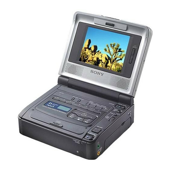
Photo : GV-D800E
GV-D800/D800E
4.0 inches
SPECIFICATIONS
Input/output
connectors
S video input
4-pin mini DIN
Luminance signal: 1 Vp-p, 75 ohms,
unbalanced
GV-D200/D800:
Chrominance signal: 0.286 Vp-p
GV-D200E/D800E:
Chrominance signal: 0.3 Vp-p,
75 ohms, unbalanced
S video output
4-pin mini DIN
Luminance signal: 1 Vp-p, 75 ohms,
unbalanced
GV-D200/D800:
Chrominance signal: 0.286 Vp-p
GV-D200E/D800E:
Chrominance signal: 0.3 Vp-p,
75 ohms, unbalanced
Audio/Video input
AV MINIJACK
Video: 1 Vp-p, 75 ohms, unbalanced,
sync negative
Audio: 327 mV, input impedance
more than 47 kiloohms
Video output
Phono jack, 1 Vp-p, 75 ohms,
unbalanced, sync negative
Audio output
Phono jacks (2) 327 mV, output
impedance less than 1 kiloohm
RFU DC OUT
Special minijack DC 5 V
DIGITAL VIDEO CASSETTE RECORDER
For MECHANISM ADJUSTMENT, refer to
the "8mm Video MECHANICAL
ADJUSTMENT MANUAL
DV input/output
4-pin connector
Headphone jack
Stereo minijack (ø 3.5 mm)
LANC
jack
Stereo mini-minijack (ø 2.5 mm)
LCD screen (GV-D800/D800E)
Picture
4.0 type
80.6 × 60.5 mm (3 1/4 × 2 1/2 in.)
Total dot number
123,200 (560 × 220)
General
Power requirements
7.2 V (battery pack)
8.4 V (AC power adaptor)
Average power consumption
(when using the battery pack)
GV-D800/D800E only
During playback using LCD
4.9 W
During playing back when you close
the LCD panel
3.0 W
Operating temperature
0 °C to 40 °C (32 °F to 104 °F)
Storage temperature
–20 °C to +60 °C (–4 °F to +140 °F)
US Model
Canadian Model
GV-D200/D800
AEP Model
UK Model
E Model
GV-D200E/D800E
B MECHANISM
" (9-973-801-11).
Dimensions (Approx.)
GV-D200/D200E:
148 × 50 × 135 mm
(5 7/8 × 2 × 5 3/8 in.)
GV-D800/D800E:
148 × 65 × 135 mm
(5 7/8 × 2 5/8 × 5 3/8 in.) (w/h/d)
Mass (approx.)
GV-D200/D200E:
660 g (1 lb 7 oz)
GV-D800/D800E:
930 g (2 lb)
excluding the battery pack and
cassette
Supplied accessories
See page 2.
AC power adaptor
Power requirements
100 - 240 V AC, 50/60 Hz
Power consumption
23 W
Output voltage
DC OUT: 8.4 V, 1.5 A in the
operating mode
Operating temperature
0 °C to 40 °C (32 °F to 104 °F)
Storage temperature
–20 °C to +60 °C (–4 °F to +140 °F)
— Continued on next page —
Advertisement

Related Manuals for Sony GV-D200


Summary of Contents for Sony GV-D200
- Page 1 AEP Model Ver 1.0 2000. 09 UK Model E Model GV-D200E/D800E B MECHANISM Photo : GV-D800E NTSC MODEL : GV-D200/D800 For MECHANISM ADJUSTMENT, refer to PAL MODEL : GV-D200E/D800E the “8mm Video MECHANICAL Function difference table ADJUSTMENT MANUAL ” (9-973-801-11).
-
Page 2: Service Mode Display
SELF-DIAGNOSIS FUNCTION SELF-DIAGNOSIS FUNCTION SELF-DIAGNOSIS DISPLAY When problems occur while the unit is operating, the counter of the When problems occur while the unit is operating, the self-diagnosis function starts working, and displays on the LCD screen or monitor viewfinder shows a 4-digit display consisting of an alphabet and TV (Note) what to do. - Page 3 SELF-DIAGNOSIS CODE TABLE Self-diagnosis Code Block Detailed Symptom/State Correction Function Code Non-standard battery is used. Use the info LITHIUM battery. Condensation. Remove the cassette, and insert it again after one hour. Video head is dirty. Clean with the optional cleaning cassette. LOAD direction.
- Page 4 GV-D200/D200E/D800/D800E SECTION 3 BLOCK DIAGRAMS 3-1. OVERALL BLOCK DIAGRAM (1/4) ( ) : Page No. shown in ( ) indicates the page to refer on the schematic diagram. (SEE PAGE 4-45) IO-68 BOARD VC-250 BOARD(1/4) (4-26) (4-23) (1/2) (4-25) IC3701...
- Page 5 GV-D200/D200E/D800/D800E 3-2. OVERALL BLOCK DIAGRAM (2/4) ( ) : Page No. shown in ( ) indicates the page to refer on the schematic diagram. CN1105 VC-250 BOARD(2/4) DV IN/OUT (4-15) X3301 IC3301 24.576MHz (CAIN) CN929 CN1104 (4-17) TPA+,- DV SIGNAL...
- Page 6 GV-D200/D200E/D800/D800E 3-3. OVERALL BLOCK DIAGRAM (3/4) ( ) : Page No. shown in ( ) indicates the page to refer on the schematic diagram. B710-MECHA DECK FU-145 BOARD(1/2) VC-250 BOARD(3/4) (4-33) (SEE PAGE 4-56) (4-35) (4-33) CN921 M901 IC4401 IC1301...
- Page 7 GV-D200/D200E/D800/D800E 3-4. OVERALL BLOCK DIAGRAM (4/4) ( ) : Page No. shown in ( ) indicates the page to refer on the schematic diagram. (GV-D800/D800E) PD-130 LS-56 BOARD FK-78 BOARD VC-250 BOARD (4/4) (4-37) BOARD (3/3) IC4803 (SEE PAGE 4-61)
- Page 8 GV-D200/D200E/D800/D800E 3-5. POWER BLOCK DIAGRAM (1/2) ( ) : Page No. shown in ( ) indicates the page to refer on the schematic diagram. FU–145 BOARD VC–250 BOARD(1/2) DC PACK SW SHOE ON CN1301 CN921 BATT SIG EX UNREG EX UNREG...
- Page 9 GV-D200/D200E/D800/D800E 3-6. POWER BLOCK DIAGRAM (2/2) ( ) : Page No. shown in ( ) indicates the page to refer on the schematic diagram. FP-571 (FLEXIBLE) VC-250 BOARD(2/2) BT001 BATT LI3V VANADIUM (SEE PAGE 4-37) LITHIUM CN926 BATTERY IC4803 (4-37)
- Page 10 GV-D200/D200E/D800/D800E SECTION 4 PRINTED WIRING BOARDS AND SCHEMATIC DIAGRAMS 4-1. FRAME SCHEMATIC DIAGRAM (1/2) FP-247 FLEXIBLE J102 VC-250 BOARD(1/2) VIDEO CN5713 CN002 CN001 CN922 LANC_SIG LANC_SIG XVTR_MODE_SW XVTR_MODE_SW 1/16 REC/PB ANP XVTR_MODE_SW XVTR_MODE_SW LANC_SIG LANC_SIG DC OUT 2/16 PB AMP,DAC...
- Page 11 GV-D200/D200E/D800/D800E FRAME SCHEMATIC DIAGRAM (2/2) GV-D800/D800E MODEL ND901 BACK LIGHT LCD 901 4 INCH COLOR LCD UNIT LS-56 BOARD PL-53 CN5502 CN01 HARNESS CN5608 AD_6 AD_6 S5601 XVD_OUT PD-130 BOARD BLIGHT+ S001 S5602 (LCD ON/OFF) PANEL_COM LCD DRIVER(1/2) CN5506 BLIGHT-...
- Page 12 GV-D200/D200E/D800/D800E For Schematic Diagram • Refer to page 4-7 for printed wiring board. • Refer to page 4-68 for waveforms. VC-250 BOARD(1/16) NO MARK:REC/PB MODE REC/PB AMP(RF BLOCK) R :REC MODE Q3111 P :PB MODE -REF.NO.:30000 SERIES- 2SA1832F-Y/GR(TPL3) XX MARK:NO MOUNT...
- Page 13 GV-D200/D200E/D800/D800E For Schematic Diagram • Refer to page 4-7 for printed wiring board. VC-250 BOARD(2/16) PB AMP,DAC(RF,ER BLOCK) RP_4.75V TO(15/16) A_2.8V -REF.NO.:30000 SERIES- PB_RF TO(11/16,16/16) L3201 XX MARK:NO MOUNT 22uH F0_ADJ_RF_IN NO MARK:REC/PB MODE TO(16/16) R :REC MODE RF_ENV P :PB MODE...
- Page 14 GV-D200/D200E/D800/D800E For Schematic Diagram • Refer to page 4-7 for printed wiring board. • Refer to page 4-68 for waveforms. VC-250 BOARD(3/16) NO MARK:REC/PB MODE R :REC MODE DV INTERFACE (JC-1 BLOCK) P :PB MODE -REF.NO.:30000 SERIES- XX MARK:NO MOUNT...
- Page 15 GV-D200/D200E/D800/D800E For Schematic Diagram • Refer to page 4-7 for printed wiring board. VC-250 BOARD(4/16) NO MARK:REC/PB MODE R :REC MODE DV INTERFACE(JC-2 BLOCK) P :PB MODE -REF.NO.:30000 SERIES- XX MARK:NO MOUNT D_1.9V TO(15/16) D_2.8V MCDA7 MCDA7 MCDA6 R3359 R3352...
- Page 16 GV-D200/D200E/D800/D800E For Schematic Diagram • Refer to page 4-7 for printed wiring board. • Refer to page 4-68 for waveforms. VC-250 BOARD(5/16) AD CONVERTER(CH BLOCK) -REF.NO.:30000 SERIES- XX MARK:NO MOUNT FB1501 D_2.8V NO MARK:REC/PB MODE IC1505 REG_GND R :REC MODE...
- Page 17 GV-D200/D200E/D800/D800E For Schematic Diagram • Refer to page 4-7 for printed wiring board. • Refer to page 4-68 for waveforms. VC-250 BOARD(6/16) NO MARK:REC/PB MODE Y/C PROCESSOR(CL BLOCK) R :REC MODE P :PB MODE -REF.NO.:30000 SERIES- XX MARK:NO MOUNT SIGNAL PATH...
- Page 18 GV-D200/D200E/D800/D800E For Schematic Diagram • Refer to page 4-7 for printed wiring board. SIGNAL PATH VC-250 BOARD(7/16) NO MARK:REC/PB MODE LINE A/D(IN BLOCK) VIDEO SIGNAL R :REC MODE P :PB MODE -REF.NO.:30000 SERIES- CHROMA Y/CHROMA XX MARK:NO MOUNT TO(4/16,5/16, SPCK...
- Page 19 GV-D200/D200E/D800/D800E For Schematic Diagram • Refer to page 4-7 for printed wiring board. VC-250 BOARD(8/16) A_4.75V TO(15/16) LINE IN/OUT(IO BLOCK) D_2.8V -REF.NO.:30000 SERIES- TAKO_CK XX MARK:NO MOUNT TAKO_C_OUT TO(7/16) C3721 L3703 ALIGN_APC_ERROR AGC_CONT TO(5/16,7/16) TAKO_Y_OUT ACC_CONT R3732 R3731 INPUT_SEL TO(11/16,14/16)
- Page 20 GV-D200/D200E/D800/D800E For Schematic Diagram • Refer to page 4-7 for VC-250 printed wiring board. • Refer to page 4-59 for IR-38 printed wiring board. • Refer to page 4-69 for waveform. VC-250 BOARD(9/16) NO MARK:ON/OFF MODE IR(IR-BLOCK) ( ):IR ON MODE...
- Page 21 GV-D200/D200E/D800/D800E For Schematic Diagram • Refer to page 4-7 for printed wiring board. • Refer to page 4-69 for waveform. NO MARK:REC/PB MODE VC-250 BOARD(10/16) R :REC MODE MECHANISM CONTROL(VC BLOCK) P :PB MODE * :Cannot measure -REF.NO.:30000 SERIES- Note:Capacitor is mounted to the location XX MARK:NO MOUNT where R4919 is printed.
- Page 22 GV-D200/D200E/D800/D800E For Schematic Diagram • Refer to page 4-7 for printed wiring board. • Refer to page 4-69 for waveform. VC-250 BOARD(11/16) BPF_MONI TO(16/16) AUDIO I/O(AU BLOCK) NO MARK:REC/PB MODE R :REC MODE PB_RF TO(2/16,16/16) -REF.NO.:30000 SERIES- P :PB MODE...
- Page 23 GV-D200/D200E/D800/D800E For Schematic Diagram • Refer to page 4-7 for VC-250 printed wiring board. • Refer to page 4-67 for FP-249, FP-355, FP-356 printed wiring boards. • Refer to page 4-68,69 for waveforms. R4446 VC-250 BOARD(12/16) MT_5V TO(11/16,15/16) R4444 VTR_UNREG...
- Page 24 GV-D200/D200E/D800/D800E For Schematic Diagram • Refer to page 4-7 for printed wiring board. • Refer to page 4-69 for waveforms. VC-250 BOARD(13/16) REG_GND MECHA CONTROL(MC BLOCK) TO(15/16) FB4501 -REF.NO.:30000 SERIES- D_2.8V R4514 XX MARK:NO MOUNT C4506 100k 0.01u NO MARK:REC/PB MODE...
- Page 25 GV-D200/D200E/D800/D800E For Schematic Diagram • Refer to page 4-7 for VC-250 printed wiring board. • Refer to page 4-67 for FP-571 printed wiring board. • Refer to page 4-69 for waveforms. VC-250 BOARD(14/16) HI CONTROL(HI BLOCK) (NOT USE) -REF.NO.:30000 SERIES-...
- Page 26 GV-D200/D200E/D800/D800E For Schematic Diagram • Refer to page 4-7 for printed wiring board. VC-250 BOARD(15/16) NO MARK:REC/PB MODE DC/DC CONVERTER(DD BLOCK) R :REC MODE P :PB MODE -REF.NO.:30000 SERIES- XX MARK:NO MOUNT CN921 MT_5V TO(11/16,12/16) CAP_VS CAP_VS CAP_VS DRUM_VS DRUM_VS...
- Page 27 GV-D200/D200E/D800/D800E For Schematic Diagram • Refer to page 4-7 for printed wiring board. CN923 VC-250 BOARD(16/16) GV-D800/800E CN933 MODEL ONLY SP_R_+ TO(3/16,13/16) CONNECTION(CN BLOCK) AFC_F0 SP_R_- TO(6/16,10/16) AFC_F0 -REF.NO.:30000 SERIES- REG_GND REG_GND TO(14/16) BPF_MONI BPF_MONI XX MARK:NO MOUNT BL_CONT BL_CONT...
- Page 28 GV-D200/D200E/D800/D800E R103 CN105 R101 R133 D111 XVTR_MODE_SW L103 100uH MA8082-(K8).S0 IO-68 BOARD 2520 LANC_SIG J102 L104 100uH 2520 AV IN/OUT FB101 XLANC_JACK_IN R106 REG_GND R107 -REF.NO.:10000 SERIES- C102 R105 R102 R134 C110 C104 AUDIO C107 REG_GND 0.001u C103 C101 0.001u 0.001u...
- Page 29 GV-D200/D200E/D800/D800E For Schematic Diagram • Refer to page 4-7 for printed wiring board. FU-145 BOARD DC/DC CONVERTER L1317 L1318 22uH 4.7uH -REF.NO.:10000 SERIES- C1347 XX MARK:NO MOUNT Q1309 CN1301 C1332 CPH6702-TL C1344 4.7u 4.7u NO MARK:REC/PB MODE SWITCHING CAP_VS GV-D800/D800E MODEL ONLY...
- Page 30 GV-D200/D200E/D800/D800E For Schematic Diagram • Refer to page 4-51 for printed wiring board. • Refer to page 4-69 for waveforms. PD-130 BOARD(1/2) (GV-D800/800E MODEL ONLY) LCD DRIVER -REF.NO.:10,000 SERIES L5504 L5503 10uH 10uH XX MARK:NO MOUNT NO MARK:REC/PB MODE C5513 C5514 0.1u...
- Page 31 GV-D200/D200E/D800/D800E For Schematic Diagram • Refer to page 4-51 for PD-130 printed wiring board. • Refer to page 4-54 for LS-56 printed wiring board. PD-130 BOARD(2/2) (GV-D800/800E MODEL ONLY) BACK LIGHT LS-56 BOARD BRIGHT+ BRIGHT- -REF.NO.:10000 SERIES- LCD SWITCH S5601...
- Page 32 GV-D200/D200E/D800/D800E CONTROL SWITCH BLOCK (FK-78) -REF.NO.:40000 SERIES- D001 SML-211UT-T86 R022 XX MARK:NO MOUNT (REC) 1608 D003 SML-211YT-T86 R024 (CAUTION) 1608 D002 SML-211DT-T86 R023 (PAUSE) D_2.8V 1608 XREC_LED XCAUTION_LED R101 S007 S008 S009 S010 S011 XPAUSE_LED VC250 BOARD(16/16) R102 KEY_AD1 PAUSE...
- Page 33 GV-D200/D200E/D800/D800E EX-36 BOARD MULTI CONNECTOR -REF.NO.:10000 SERIES- CN204 CN203 VIDEO_OUT VIDEO_GND VIDEO_OUT_GND V/Y_IN V/Y_IN V/Y_IN_GND VIDEO_IN_GND AUDIO_R_IN AUDIO_R_IN AUDIO_R_IN_GND AUDIO_L_IN AUDIO_L_IN AUDIO_IN_GND AUDIO_L_IN_GND LANC_SIG LANC_SIG IO_GND LANC_GND LANC_GND MULTI CONNECTOR EX_GND VIDEO_GND EX_GND VIDEO_OUT AUDIO_R_OUT VIDEO_OUT_GND AUDIO_L_OUT AUDIO_R_OUT AUDIO_OUT_GND VC-250...
- Page 34 GV-D200/D200E/D800/D800E FP-571 (BATTERY), FP-249 (S/T REEL) PRINTED WIRING BOARDS 4-3. WAVEFORMS — Ref. No. FP-571, FP-249 Boards; 20,000 Series — • Refer to page 4-37 for FP-571 schematic diagram. VC-250 BOARD • Refer to page 4-33 for FP-249, FP-355, FP-356 schematic diagrams.
- Page 35 GV-D200/D200E/D800/D800E VC-250 PD-130 BOARD BOARD IC5501 w; IC5502 wh IC4401 ed IC4902 1 2.8Vp-p 2.8Vp-p 3.6Vp-p 3.6Vp-p 0.6 sec 85 nsec 50 nsec IC5501 ws IC4401 ra IC5701 qf 2.8Vp-p 250mVp-p 1.1 sec 300 nsec 3.7Vp-p IC4401 tj,tl,ya IC3901 ws IR ON IC5501 wf 3.4Vp-p...
- Page 36 GV-D200/D200E/D800/D800E SECTION 5 ADJUSTMENTS Before starting adjustment EVR Data Re-writing Procedure When Replacing Board The data that is stored in the repair board, is not necessarily correct. Perform either procedure 1 or procedure 2 or procedure 3 when replacing board.
- Page 37 1-1. Adjusting items when replacing main parts and boards. When replacing main parts, adjust the items indicated by z in the following table. *1: When replacing the drum assy. or mechanism deck, reset the data of page: 2, address: A2 to A4 to “00”. (Refer to “Record of Use check” of “5-4.
-
Page 38: Adjustment Preparations
5-1. ADJUSTMENT PREPARATIONS For details of the adjustment remote commander, refer to “5-4. SERVICE MODE”. With 4-inch LCD panel: GV-D800/D800E Without 4-inch LCD panel: GV-D200/D200E 1-1. PREPARATIONS BEFORE ADJUSTMENT 1-1-1. List of Service Tools • Oscilloscope • Regulated power supply •... -
Page 39: Mechanism Section
ADJUSTMENT Mechanism Section adjustments, checks, and replacement of mechanism parts, refer to the separate volume “8mm Video Mechanism Adjustment Manual B Mechanism ”. Note 1: NTSC model: GV-D200/D800 2-1-2. TAPE PATH ADJUSTMENT PAL model: GV-D200E/D800E 1. Preparations for Adjustment 2-1. - Page 40 2-2. DIGITAL8 MODE 2-2-3. OVERALL TAPE PATH CHECK 2-2-1. HOW TO ENTER RECORD MODE WITHOUT 1. Recording of the tape path check signal CASSETTE Clean the tape running side (tape guide, capstan shaft, pinch roller). Connect the adjustment remote commander to the LANC jack. Input a color bar signal to the AUDIO/VIDEO INPUT jack.
-
Page 41: Electrical Adjustment
For details of the adjustment remote commander, refer to “5-4. SERVICE MODE”. 3-1. PREPARATIONS BEFORE ADJUSTMENTS Use the following measuring instruments for video section adjustments. Note: NTSC model:GV-D200/D800 PAL model: GV-D200E/D800E 3-1-1. Equipment to Required 1) TV monitor 13) PAL Hi8/standard8 alignment tapes (For PAL model) 2) Oscilloscope (dual-phenomenon, band width above 30 MHz •... - Page 42 3-1-2. Precautions on Adjusting 3-1-3. Adjusting Connectors Disconnecting the VC-250 board CN926 (4P, 0.8mm) means Some of the adjusting points of the video section are concentrated disconnecting the lithium 3V power supply (FP-571 board at VC-250 board CN933. Connect the measuring instruments via BT001), data such as date, time, user-set menus will be lost.
- Page 43 3-1-4. Connecting the Equipment Connect the measuring instruments as shown in Fig. 5-3-2, and perform the adjustments. LANC jack Pattern generator Adjustment VIDEO remote (Yellow) Video output commander (75 Ω ) AUDIO L (White) Main unit AUDIO R (Red) AUDIO/VIDEO INPUT jack VIDEO OUTPUT jack TV monitor...
- Page 44 3-1-5. Alignment Tape The following table lists alignment tapes which are available. Use the tape specified in the signal column for each adjustment. If the type of tape to be used for checking operations is not specified, use whichever type. Digital8 alignment tape Name Usage...
- Page 45 Fig. 5-3-3. Shows the color bar signals recorded on the alignment tape. Note : Measure using the VIDEO terminal (Terminated at 75 Ω). For NTSC model White (100%) White (75%) Burst signal 0.714V (75%) 0.286V Black 0.286V White (100%) Horizontal sync signal Color bar signal waveform Color bar pattern For PAL model...
- Page 46 3-2. INITIALIZATION OF C, D, E, F, 7, 8 PAGE Processing after Completing Modification of C, D, 8 Page data DATA Order Page Address Data Procedure Set the data 3-2-1. INITIALIZATION OF C, D, 8 PAGE DATA Set the data, and press the PAUSE button.
- Page 47 4. D Page Table Initial value Address Remark Note: Fixed data-1: Initialized data. (Refer to “1. Initializing the C, D, 8 NTSC PAL Page Data”.) 93 to 99 Fixed data-1 Fixed data-2: Modified data. (Refer to “2. Modification of C, D, 8 Page Data”).
- Page 48 5. 8 Page Table Initial value Address Remark Note: Fixed data-1: Initialized data. (Refer to “1. Initializing the C, D, 8 NTSC PAL Page Data”.) Fixed data-2 Fixed data-2: Modified data. (Refer to “2. Modification of C, D, 8 Page Data”). 6A to 83 Fixed data-1 Fixed data-2...
- Page 49 Order Page Address Data Procedure Set the data. Fixed data-2 Set the following data. 1D to 22 Fixed data-1 55: GV-D200/D800 (NTSC) Fixed data-2 51: GV-D200E/D800E (PAL) Set the following data, and press Fixed data-1 PAUSE button. Fixed data-2 55: GV-D200/D800 (NTSC)
- Page 50 4. E Page Table Initial value Address Remark Note: Fixed data-1: Initialized data. (Refer to “1. Initializing the E, F, 7 NTSC PAL Page Data”.) Fixed data-2 Fixed data-2: Modified data. (Refer to “2. Modification of E, F, 7 Page Data”). 95 to 97 Fixed data-1 Fixed data-2...
- Page 51 5. 7 Page Table Address Remark Note: Fixed data-1: Initialized data. Fixed data-2 (Refer to “1. Initializing the E, F, 7 Page Data”.) Fixed data-2: Modified data. (Refer to “2. Modification of E, F, 7 Page Data”). Fixed data-1 Address Remark Fixed data-2 00 to 05...
- Page 52 3-3. SYSTEM CONTROL SYSTEM ADJUSTMENT 1-2. Serial No. Input Write the serial No. and model code in the EEPROM (nonvolatile memory). Convert the serial No. on the name plate from decimal to 1. Serial No. Input hexadecimal, and write in the EEPROM. 1-1.
- Page 53 Hexa- Hexa- Hexa- Hexa- Hexa- Hexa- Hexa- Hexa- Decimal Decimal Decimal Decimal Decimal Decimal Decimal Decimal decimal decimal decimal decimal decimal decimal decimal decimal 0000 8192 2000 16384 4000 24576 6000 32768 8000 40960 A000 49152 C000 57344 E000 0100 8448 2100 16640...
- Page 54 2. Battery End Adjustment Set the battery end voltage. If the voltage is incorrect, the life of the battery will shorten. The image at the battery end will also be rough. Mode Playback Signal Arbitrary Measurement Point Display data of page: 2, address: 5D Measuring Instrument Adjustment remote commander Adjustment Page...
- Page 55 3-4. SERVO AND RF SYSTEM ADJUSTMENT 2. PLL fo & LPF fo Pre-Adjustment (VC-250 Board) Before perform the servo and RF system adjustments, check that the specified value of “27MHz Origin Oscillation Adjustment” of Mode VTR stop “VIDEO SYSTEM ADJUSTMENT” is satisfied. Measurement Point Display data of page: 3, address: 03 Measuring Instrument...
- Page 56 3. Switching Position Adjustment (VC-250 Board) 4. AGC Center Level and APC & AEQ Adjustment To obtain normal playback waveform output during the Digital8 4-1. Preparations before adjustments playback mode, adjust the switching position. Mode VTR playback Mode Recording Signal SW/OL reference tape (WR5-2D) Signal Color bar...
- Page 57 4-3. APC & AEQ Adjustment (VC-250 Board) 4-4. Processing after Completing Adjustments Order Page Address Data Procedure Mode Playback Signal Recorded signal at “Preparations Set the data. before adjustments” Set the data. Measurement Point Pin qh of CN933 (RF MON) (Note 1) Set the data.
- Page 58 5. PLL fo & LPF fo Final Adjustment (VC-250 Board) 6. Hi8/Standard8 Switching Position Adjustment (VC-250 Board) If deviated in this case causes switching noise or jitter on the Hi8/ Mode VTR stop Standard8 mode played back screen. Signal Arbitrary Mode Playback Measurement Point...
- Page 59 7. CAP FG Offset Adjustment (VC-250 board) Set the Cap FG signal duty cycle to 50% to establish an appropriate capstan servo. If deviated, the uneven rotation of capstan and noise can occur in the Hi8/Standard8 LP mode. Mode Playback Signal Hi8/standard 8 alignment tape : For checking operation...
- Page 60 3-5. VIDEO SYSTEM ADJUSTMENTS 2. Chroma BPF fo Adjustment (VC-250 Board) Set the center frequency of IC3701 chroma band-pass filter. Switch setting: Mode VTR stop DEMO MODE (Menu setting) ........OFF Signal No signal Measurement Point CH1: Chroma signal terminal of S 1.
- Page 61 3. S VIDEO OUT Y Level Adjustment (VC-250 Board) 4. S VIDEO OUT Chroma Level Adjustment (VC-250 Board) Mode VTR stop Mode VTR stop Signal No signal Signal No signal Measurement Point Y signal terminal of S VIDEO OUT Measurement Point Chroma signal terminal of S VIDEO jack (75Ω...
- Page 62 Check that the burst signal level Set the following data, and press (B) satisfies the specified value. PAUSE button. Set the data, and press PAUSE 69: GV-D200/D800 (NTSC) button. 65: GV-D200E/D800E (PAL) Set the data, and press PAUSE Set the following data, and press button.
- Page 63 7. Hi8/standard 8mm AFC fo Adjustment (VC-250 board) Adjust the pull-in range of the clock generator (IC2201) for A/D conversion during Hi8/standard 8mm playback. Mode VTR stop Signal No signal Measurement Point Pin 2 of CN933 (AFC f0) Measuring Instrument Digital voltmeter Adjustment Page Adjustment Address...
- Page 64 3-6. IR TRANSMITTER ADJUSTMENTS Adjust using the IR receiver jig (J-6082-383-A). Note: If the distance between the IR receiver jig and the VCR is below 1m, cover the LASER LINK emitter with a ND filter. (For example, when the distance is 30cm to 50cm, cover the LASER LINK emitter with a ND filter 1.0.) Switch setting: LASER LINK ........
- Page 65 3. IR Audio Deviation Adjustment (VC-250 board) Mode VTR stop Signal Video : No signal Audio : –400Hz, –7.5dBs, Audio left and right terminal of AUDIO/VIDEO jack Measurement Point AUDIO L terminal and AUDIO R terminal of IR receiver jig (Terminated at 47kΩ) Measuring Instrument Audio level meter...
- Page 66 3-7. AUDIO SYSTEM ADJUSTMENTS 1. Hi8/Standard8 AFM BPF fo Adjustment (VC-250 board) Sets the BPF passing frequency of IC760 so that the AFM signal [Connecting the measuring instruments for the audio] can separate from the playback RF signal properly. If deviated. the Connect the audio system measuring instruments in addition to the mono/stereo mode will be differentiated incorrectly, and noises and video system measuring instruments as shown in Fig.
- Page 67 2. Hi8/Standard8 AFM 1.5 MHz Deviation Adjustment 4. Digital8 Playback Level Check (VC-250 board) Mode Playback Adjust to the optimum 1.5MHz audio FM signal deviation. Signal Digital8 alignment tape: If the adjustment is not correct, its playback level will differ from For audio operation check that of other units.
- Page 68 7. Overall Noise Level Check 8. Overall Separation Check Mode Recording and playback Mode Recording and playback Signal No signal: Audio terminal left and Signal No signal: Audio terminal <left> right of AUDIO/VIDEO INPUT jack [right] of AUDIO/VIDEO INPUT jack Measurement Point AUDIO OUT jack LEFT or RIGHT 400Hz, –7.5dBs signal: Audio...
- Page 69 3-8. LCD SYSTEM ADJUSTMENT 1. LCD Initial Data Input (1) (GV-D800/D800E) Mode VTR stop Signal No signal Note 1: The back light (fluorescent tube) is driven by a high voltage AC Adjustment Page power supply. Therefore, do not touch the back light holder to avoid electrical shock.
- Page 70 2. LCD Initial Data Input (2) 3. VCO Adjustment (PD-130 board) Set the VCO free-run frequency. If deviated, the LCD screen will Mode VTR stop be blurred. Signal No signal Mode VTR stop Adjustment Page Signal No signal Adjustment Address A0 to B1 Measurement Point Pin 8 of CN5502 (XHD OUT)
- Page 71 4. RGB AMP Adjustment (PD-130 board) 5. Contrast Adjustment (PD-130 board) Set the D range of the RGB decoder used to drive the LCD to the Set the level of the VIDEO signal for driving the LCD to the specified specified value.
- Page 72 6. COM AMP Adjustment (PD-130 board) 7. V-COM Adjustment (PD-130 board) Set the common electrode drive signal level of LCD to the specified Set the DC bias of the common electrode drive signal of LCD to the value. specified value. If deviated, the LCD display will move, producing flicker and Mode VTR stop...
- Page 73 8. White Balance Adjustment (PD-130 board) Correct the white balance. If deviated, the reproduction of the LCD screen may degenerate. Mode VTR stop Signal No signal Measurement Point Check on LCD screen Measuring Instrument Adjustment Page Adjustment Address A8, A9 Specified Value The LCD screen should not be colored.
-
Page 74: Service Mode
5-4. SERVICE MODE 4-1. ADJUSTMENT REMOTE COMMANDER 2. Precautions Upon Using the Adjustment Remote Commander The adjustment remote commander is used for changing the calculation coefficient in signal processing, EVR data, etc. The Mishandling of the adjustment remote commander may erase the correct adjustment data at times. - Page 75 4-2. DATA PROCESS The calculation of the DDS display and the adjustment remote commander display data (hexadecimal notation) are required for obtaining the adjustment data of some adjustment items. In this case, after converting the hexadecimal notation to decimal notation, calculate and convert the result to hexadecimal notation, and use it as the adjustment data.
- Page 76 4-3. SERVICE MODE 2. Emergence Memory Address 2-1. C Page Emergence Memory Address Additional note on adjustment Note: After the completion of the all adjustments, cancel the service mode Page C Address F4 to FF by either of the following ways. 1) After data on page: D and F is restored, unplug the main power Address Contents...
- Page 77 2-2. F Page Emergence Memory Address 2-3. EMG Code (Emergency Code) Note 1: Emergence of PB mode only. Codes corresponding to the errors which occur are written in C page, addresses F4, F8 and FC (or F page, addresses 10, 14 and 18). The type of error indicated by the code are shown in the following Page F Address 10 to 1B...
- Page 78 2-4. MSW Code • The lower parts of the data of C page, addresses F6, FA and FE (or F page, addresses 12, 16 and 1A) represent the MSW codes (mode switch mechanism position) when errors occurs. • The upper parts of the data of C page, addresses F6, FA and FE (or F page, addresses 12, 16 and 1A) represent, when the mechanism position is to be moved, the MSW codes at the start movement (when moving the loading motor).
- Page 79 3. Bit Value Discrimination Bit values must be discriminated using the display data of the Display on the Bit values adjustment remote commander for the following items. Us the table adjustment bit3 bit2 bit1 bit0 below to discriminate if the bit value is “1” or “0”. remote commander bit7...
- Page 80 7. Switch check (4) Page 2 Address 60, 61, 62, 65, 66 Using method: Select page: 2, address: 60, 61, 62, 65, 66. By discriminating the display data, the pressed key can be discriminated. Data Address 00 to 0C 0D to 24 25 to 3F 40 to 5D 5E to 81...
- Page 81 9. Record of Self-diagnosis check Page 2 Address B0 to C6 Address Self-diagnosis code “Repaired by” code (Occurred 1st time) *1 “Block function” code (Occurred 1st time) “Detailed” code (Occurred 1st time) “Repaired by” code (Occurred 2nd time) *1 “Block function” code (Occurred 2nd time) “Detailed”...