Yamaha YDS-12 Service Manual
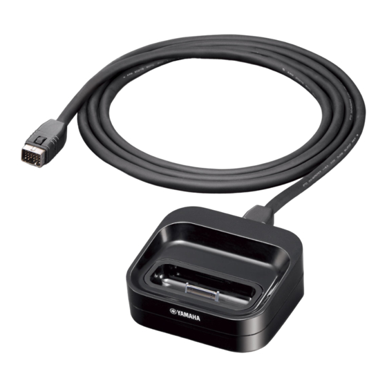
Universal dock for ipod
Hide thumbs
Also See for YDS-12:
- Owner's manual (80 pages) ,
- Owner's manual (11 pages) ,
- Owner's manual (17 pages)
Table of Contents
Advertisement
Quick Links
•
MODE switch setting
1. When checking operation, the mode switch of this unit properly corresponding MUST be set to the dock-compatible
component connected to this unit.
Position A: For the YDS-12 compatible component (the RX-V367 or later)
Position B: For the Dock-compatible component sold in 2009 or before
2. After repairing is completed, the mode switch of this unit MUST be set to "A" position.
・ モードスイッチの設定
1. 動作チェックする場合、本機に接続した DOCK 対応機器に対応
して本機のモードスイッチを正しくセットしてください。
ポジション A:YDS-12 対応機器(RX-V367 以降)
ポジション B:2009 年度以前に発売された DOCK 対応機器
2. 修理完了後、本機のモードスイッチを A の位置にセットして
ください。
This manual has been provided for the use of authorized YAMAHA Retailers and their service personnel.
It has been assumed that basic service procedures inherent to the industry, and more specifi cally YAMAHA Products, are already known
and understood by the users, and have therefore not been restated.
WARNING:
IMPORTANT:
The data provided is believed to be accurate and applicable to the unit(s) indicated on the cover. The research, engineering, and service
departments of YAMAHA are continually striving to improve YAMAHA products. Modifications are, therefore, inevitable and
specifi cations are subject to change without notice or obligation to retrofi t. Should any discrepancy appear to exist, please contact the
distributor's Service Division.
WARNING:
IMPORTANT:
■ CONTENTS
TO SERVICE PERSONNEL ............................................2
FRONT PANEL ...............................................................3
REAR PANELS ...............................................................3
SPECIFICATIONS / 参考仕様 .........................................4
INTERNAL VIEW ............................................................4
REPAIR NOTES / 修理上の留意点 ..................................5
1 0 1 1 7 1
UNIVERSAL DOCK for iPod
YDS-12
SERVICE MANUAL
IMPORTANT NOTICE
Failure to follow appropriate service and safety procedures when servicing this product may result in personal injury,
destruction of expensive components, and failure of the product to perform as specifi ed. For these reasons, we advise
all YAMAHA product owners that any service required should be performed by an authorized YAMAHA Retailer or
the appointed service representative.
The presentation or sale of this manual to any individual or fi rm does not constitute authorization, certifi cation or
recognition of any applicable technical capabilities, or establish a principle-agent relationship of any form.
Static discharges can destroy expensive components. Discharge any static electricity your body may have
accumulated by grounding yourself to the ground buss in the unit (heavy gauge black wires connect to this buss).
Turn the unit OFF during disassembly and part replacement. Recheck all work before you apply power to the unit.
DISASSEMBLY PROCEDURES / 分解手順 ...................6
IC DATA ...........................................................................7
BLOCK DIAGRAM ..........................................................8
PRINTED CIRCUIT BOARD ...........................................9
SCHEMATIC DIAGRAM ................................................ 10
REPLACEMENT PARTS LIST ...................................... 11
Copyright © 2010
This manual is copyrighted by YAMAHA and may not be copied or
redistributed either in print or electronically without permission.
Rear view / 背面
MODE switch
モードスイッチ
All rights reserved.
P.O.Box 1, Hamamatsu, Japan
'10.04
Advertisement
Table of Contents

Related Manuals for Yamaha YDS-12


Summary of Contents for Yamaha YDS-12
-
Page 1: Table Of Contents
This manual has been provided for the use of authorized YAMAHA Retailers and their service personnel. It has been assumed that basic service procedures inherent to the industry, and more specifi cally YAMAHA Products, are already known and understood by the users, and have therefore not been restated. -
Page 2: To Service Personnel
YDS-12 ■ TO SERVICE PERSONNEL AC LEAKAGE 1. Critical Components Information WALL EQUIPMENT TESTER OR OUTLET UNDER TEST EQUIVALENT Components having special characteristics are marked must be replaced with parts having specifications equal to those originally installed. 2. Leakage Current Measurement (For 120V Models Only) -
Page 3: Front Panel
YDS-12 ■ FRONT PANEL Top view Front view Side view ■ REAR PANELS Rear view Bottom view U, C models R, T, K, A, G, J models... -
Page 4: Specifications / 参考仕様
YDS-12 ■ SPECIFICATIONS / 参考仕様 ■ General / 総合 • DIMENSIONS Dimensions (W x H x D) / 寸法(幅 × 高さ × 奥行き) ......... 89 x 37 x 86 mm (3-1/2" x 1-1/2" x 3-3/8") Weight / 質量 ................. 160 g (5.64 oz.) Finish / 仕上げ... -
Page 5: Repair Notes / 修理上の留意点
The MAIN P.C.B. must be replaced as a whole in case of a failure. 2. Operation check 2. 動作確認 YDS-12 does not operate by itself. YDS-12 は単独で動作しません。 To check its operation, prepare the Dock-compatible 動作チェックする場合、DOCK 対応機器(AV レシー component (AV receiver, etc. (*1)) and type of the バーなど)および、iPod/iPhone(※... -
Page 6: Disassembly Procedures / 分解手順
YDS-12 ■ DISASSEMBLY PROCEDURES / 分解手順 1. Removal of MAIN P.C.B. 1. MAIN P.C.B. の外し方 a. Remove 3 screws ( ① ). (Fig. 1) a. ① のネジ 3 本を外します。 (Fig. 1) Screws ( ① ) are identified with ( ⇒ ) marks. (Fig. 1) ※... -
Page 7: Ic Data
XOUT clock output XIN clock input Power supply input MODE MODE H : Normal mode, L : Flash rewrite mode RXD1 RXD1 RS232C receive data input P1_7 DOCK_ID Dock_ID input (YDS-12/YDS-11) CLK0 CLK0 SPI_CLK RXD0 RXD0 SPI_SOMI TXD0 TXD0 SPI_SIMO P1_3... -
Page 8: Block Diagram
YDS-12 ■ BLOCK DIAGRAM USB_VBUS +VCC PWR+ +3.3V Regulator UGND DGND Authentication IC MODE SWITCH (+3.3V, UGND) 13 14 DOCK_ID MODE SWITCH DETECT ACCPWR_IPD ACCPWR_RCV Microprocessor (+3.3V, UGND) IC3, 4 Multiplexer RX_IPD TX_RCV (+3.3V, UGND) TX_IPD RX_RCV IPOD_DET IPOD_DET AUDIO_L... -
Page 9: Printed Circuit Board
YDS-12 ■ PRINTED CIRCUIT BOARD FOR INFORMATION ONLY (NO REPLACEMENT COMPONENT PARTS WILL BE AVAILABLE) MAIN P.C.B. MAIN P.C.B. (Side A) (Side B) MODE switch DOCK (To receiver) • Semiconductor Location • Semiconductor Location Ref no. Location Ref no. Location... -
Page 10: Schematic Diagram
YDS-12 ■ SCHEMATIC DIAGRAM FOR INFORMATION ONLY (NO REPLACEMENT COMPONENT PARTS WILL BE AVAILABLE) POINT B 1 / IC5 (7 pin, VCC), 2 / IC5 (3 pin, RESET) The voltage is measured with the dock-compatible component. 電圧はDOCK対応機器を接続して測定したものです。 POINT A XL1 (Pin 4 of IC5) -
Page 11: Replacement Parts List
YDS-12 ■ REPLACEMENT PARTS LIST • OVERALL ASS'Y Ref No. Part No. Description Remarks Markets 部 品 名 ランク WU907500 P.C.B. ASS'Y MAIN PCB MAIN WU898200 TOP CABINET トップキャビネット WR513800 SPRING IPOD スプリングiPod WU898400 BOTTOM CABINET JRTKAG ボトムキャビネット WU920600 BOTTOM CABINET ボトムキャビネット WV240800 CONNECTOR SUPPORT コネクターサポート ... - Page 12 YDS-12...