Yamaha PORTATONE PSR-540 Service Manual
Hide thumbs
Also See for PORTATONE PSR-540:
- Vejledning (157 pages) ,
- Owner's manual (160 pages) ,
- Manual de instrucciones (161 pages)
Table of Contents
Advertisement
Quick Links
SERVICE MANUAL
CONTENTS
SPECIFICATIONS ...................................................................................... 3
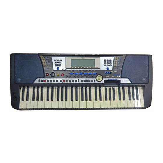
PANEL LAYOUT ....................................................................................... 4
CIRCUIT BOARD LAYOUT ....................................................................... 5
Block Diagram .................................................................................... 6
DISASSEMBLY PROCEDURE ................................................................. 7
Lsi Pin Description ............................................................................ 9
Ic Block Diagram ............................................................................. 11
CIRCUIT BOARDS .................................................................................. 12
TEST PROGRAM & INITIALIZE ............................................................... 16
MIDI IMPLEMENTATION CHART ............................................................ 18
PARTS LIST
PK
001629
HAMAMATSU,JAPAN
1.45K-536 I Printed in Japan'99.06
Advertisement
Table of Contents

Related Manuals for Yamaha PORTATONE PSR-540


Summary of Contents for Yamaha PORTATONE PSR-540
- Page 1 SERVICE MANUAL CONTENTS SPECIFICATIONS ..................3 PANEL LAYOUT ..................4 CIRCUIT BOARD LAYOUT ............... 5 BLOCK DIAGRAM ..................6 DISASSEMBLY PROCEDURE ..............7 LSI PIN DESCRIPTION ................9 IC BLOCK DIAGRAM ................11 CIRCUIT BOARDS .................. 12 TEST PROGRAM & INITIALIZE ............... 16 MIDI IMPLEMENTATION CHART ............
- Page 2 PSR-540 28CA1-8813687...
- Page 3 PSR540 HG73C205AFD (XU947C00) SWX00B TONE GENERATOR (DM IC200) NAME FUNCTION NAME FUNCTION Initial clear CMA3 Program address bus RFCLKI PLL Clock CMA8 Program address bus PLL Control CMA2 Program address bus AVDD_PLL Power supply read signal AVSS_PLL Ground CMA1 Program address bus MODE0 SWX dual mode high byte effective signal...
- Page 4 PSR540 HD63266F (XI939A00) FDC (Floppy Disk Controller) (DM IC800) NAME FUNCTION NAME FUNCTION 8"//5" Data transmission speed /TRKO Track 00 signal XTALSET Clock select /INDEX Index signal /RESET Rest /RDATA Read data input from FDD E//RD Enable/Read XTAL2 Clock RW//WR Read/write/Write EXTAL2 Chip select...
- Page 5 PSR-540 KS0066U-10B(XV226A00) LCD DRIVER (PN IC100) NAME FUNCTION NAME FUNCTION Data interface Segment signal output for LCD driving Common signal output for LCD driving Ground OSC1 Oscillator OSC2 Oscillator Power supply CLK1 Data latch clock Segment signal output for LCD CLK2 Data shift clock driving...
- Page 6 PSR-540 014: Output R Connect the level meter (with a JIS-C filter) to the [PHONE/AUX OUT] jack. (33 1. TEST PROGRAM ohm load) A. PREPARATION Set the [MASTER VOLUME] at maximum. PA-6 (AC adapter) is used. Check the output level (1kHz). Phones L: Less than -60.0 dBm The volume is usually moved to the use position when no volume change is required.
-
Page 7: Data Initialization
PSR-540 2. INITIALIZE Except for the data listed below, all PSR-540 panel settings are reset to their initial settings whenever the power is turned on. The data listed below are backed up (i.e. retained in the memory) as long as either an AC adaptor is connected or a set of batteries is installed. - Page 8 PSR-540 Note: See parts list for details of circuit board component parts.
- Page 9 PSR-540 WARNING Components having special characteristics are marked and must be replaced with parts having specification equal to those originally installed. Note: See parts list for details of circuit board component parts.