Sony MDS-JE510 Service Manual
Minidisc deck
Hide thumbs
Also See for MDS-JE510:
- Operating instructions manual (37 pages) ,
- Limited warranty (1 page) ,
- Operating instructions manual (35 pages)
Table of Contents
Advertisement
Advertisement
Table of Contents

Related Manuals for Sony MDS-JE510


Summary of Contents for Sony MDS-JE510
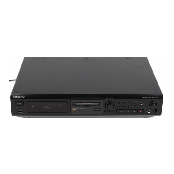
- Page 1 MDS-JE510 SERVICE MANUAL US Model Canadian Model AEP Model UK Model E Model Photo: AEP model Model Name Using Similar Mechanism MDS-JE500 MD Mechanism Type MDM-3A/3B Optical Pick-up Type KMS-260A/J1N SPECIFICATIONS — Continued on next page — MINIDISC DECK MICROFILM...
- Page 2 VAROITUS FONCTIONNEMENT. NE REMPLACER CES COMPOSANTS Parist voi räjähtää, jos se on virheellisesti asennettu. QUE PAR DES PIÈCES SONY DONT LES NUMÉROS Vaihda paristo ainoastaan laitevalmistajan suosittelemaan tyyppiin. SONT DONNÉS DANS CE MANUEL OU DANS LES Hävitä käytetty paristo valmistajan ohjeiden mukaisesti.
-
Page 3: Table Of Contents
SAFETY CHECK-OUT TABLE OF CONTENTS After correcting the original service problem, perform the follow- 1. SERVICING NOTE ............4 ing safety checks before releasing the set to the customer: Check the antenna terminals, metal trim, “metallized” knobs, screws, 2. GENERAL ................ -
Page 4: Servicing Note
SECTION 1 SERVICING NOTE JIG FOR CHECKING BD BOARD WAVEFORM The special jig (J-2501-124-A) is useful for checking the waveform of the BD board. The names of terminals and the checking items to be performed are shown as follows. I+3V : For measuring IOP (Check the deterioration of the optical pick-up laser) IOP : For measuring IOP (Check the deterioration of the optical pick-up laser) TEO : TRK error signal (Traverse adjustment) : Reference level for checking the signal... - Page 5 RETRY CAUSE DISPLAY MODE • In this test mode, the causes for retry of the unit during recording can be displayed on the fluorescent display tube. This is useful for locating the faulty part of the unit. • The data amount stored in D RAM, number of retries, and retry cause are displayed. Each is displayed in hexadecimal number. •...
- Page 6 Reading the Retry Cause Display Higher Bits Lower Bits Hexa- Hexadecimal Cause of Retry Occurring conditions decimal b7 b6 b5 b4 b3 b2 b1 b0 Binary Spindle is slow When spindle rotation is detected as slow (Not used) (Not used) When ADER was counted more than ader5 five times continuously...
-
Page 7: General
SECTION 2 GENERAL Location of Parts and Controls 9 10 11 POWER switch 13 PHONE LEVEL knob Remote sensor 14 PHONES jack 15 r REC (recording) button Display window 16 p (stop) button Disc compartment AMS knob 17 REPEAT button 18 P (pause) button DISPLAY/CHAR button 0/) buttons... - Page 8 This section is extracted from instruction manual. — 8 —...
- Page 9 — 9 —...
- Page 10 — 10 —...
- Page 11 — 11 —...
- Page 12 — 12 —...
- Page 13 — 13 —...
- Page 14 — 14 —...
- Page 15 — 15 —...
- Page 16 — 16 —...
- Page 17 — 17 —...
- Page 18 — 18 —...
- Page 19 — 19 —...
-
Page 20: Bracket (T), (L) And (R)
SECTION 3 DISASSEMBLY Note : Follow the disassembly procedure in the numerical order given. 4 Case 3-1. CASE AND FRONT PANEL ASSEMBLY 3 Screw 1 Two screws 2 Two screws claw 0 Remove the front panel assembly releasing two claws. 7 Flat type wire (CN303) 5 Screw... -
Page 21: Bd Board
3-3. BD BOARD 2 Flat type wire (15 core) 4 OP relay flexible board 1 Flexible board (Over write head) 5 BD board 3 Screw (BVTT2x4) 3-4. SUB CHASSIS 1 Two step screws 2 Two step screws 3 Two insulators 4 Two insulators Part A Part A... -
Page 22: Shutter Assembly
3-5. SHUTTER ASSEMBLY 1 Stopper washer Shutter assembly Shaft (lid) 2 Shaft (shutter) 3 Shutter assembly Hole B Shaft (shutter) Hole A When installing, install the shaft (shutter) into the hole A as shown in the figure before installing the shaft (lid) into the hole B. -
Page 23: Slider Complete Assembly
3-7. SLIDER COMPLETE ASSEMBLY 3 Set the shaft of Gear (LA) to be at the claw position in the figure. claw 45° 4 Remove the slider complete assembly 1 Screw in the direction of arrow with putting (M1.7x2) 2 Retainer (gear) out of two claws. -
Page 24: Test Mode
SECTION 4 TEST MODE 4-1. PRECAUTIONS FOR USE OF TEST MODE 1 As loading related operations will be performed regardless of the test mode operations being performed, be sure to check that the disc is stopped before setting and removing it. Even if the §EJECT button is pressed while the disc is rotating during continuous playback, continuous recording, etc., the disc will not stop rotating. - Page 25 4-5-1. Operating the Continuous Playback Mode 1. Entering the continuous playback mode 1 Set the disc in the unit. (Whichever recordable discs or discs for playback only are available.) 2 Rotate the AMS knob and display “CPLAY MODE”. 3 Press the YES button to change the display to “CPLAY IN”. 4 When access completes, the display changes to “C1 = AD = ”.
- Page 26 4-6. FUNCTIONS OF OTHER BUTTONS Function Contents Sets continuous playback when pressed in the STOP state. When pressed during continuous playback, the tracking servo turns ON/OFF. Stops continuous playback and continuous recording. The sled moves to the outer circumference only when this is pressed. The sled moves to the inner circumference only when this is pressed.
-
Page 27: Electrical Adjustments
SECTION 5 ELECTRICAL ADJUSTMENTS 5-1. PRECAUTIONS FOR CHECKING LASER DIODE 5-3. PRECAUTIONS FOR ADJUSTMENTS EMISSINON 1) When replacing the following parts, perform the adjustments and checks with ¬ in the order shown in the following table. To check the emission of the laser diode during adjustments, never view directly from the top as this may lose your eye-sight. - Page 28 5-6. LASER PPOWER ADJUSTMENT 5-5. TEMPERATURE COMPENSATION OFFSET Connection : ADJUTMENT Laser power Save the temperature data at that time in the non-volatile memory meter as 25 ˚C reference data. Note : 1. Usually, do not perform this adjustment. 2. Perform this adjustment in an ambient temperature of 22 ˚C to Optical pick-up 28 ˚C.
- Page 29 5-7. TRAVERSE ADJUSTMENT 11. Rotate the AMS knob until the waveform of the oscilloscope moves closer to the specified value. Connection : In this adjustment, waveform varies at intervals of approx. 2%. Oscilloscope Adjust the waveform so that the specified value is satisfied as much as possible.
- Page 30 5-8. FOCUS BIAS ADJUSTMENT 5-9. ERROR RATE CHECK 5-9-1. CD Error Rate Check Adjusting Method : 1. Load a continuously recorded disc (Refer to “5-4. Creating Con- Checking Method : tinuously Recorded Disc”.). 1. Load a check disc (MD) TDYS-1. 2.
-
Page 31: Circuit Boards Location
SECTION 6 DIAGRAMS 5-11. ADJUSTING POINTS AND CONNETING POINTS 6-1. CIRCUIT BOARDS LOCATION [BD BOARD] (SIDE A) 5 CN110 NOTE I + 3V BD board SW board CN101 MAIN board DISPLAY board D101 IC192 [BD BOARD] (SIDE B) EJECT SW board HP board CONTROL (SW) board IC171... - Page 32 MDS-JE510 6-2. BLOCK DIAGRAMS — BD SECTION — DIGITAL SERVO SIGNAL PROCESSOR, DIGITAL SIGNAL PROCESSOR OVER WRITE HEAD DRIVE EFM/ACIRC ENCODER/DECODER, SHOCK-PROOF MEMORY CONTROLLER, IC181 ATRAC ENCODER/DECODER, 2M-BIT DRAM IC121 SCTX XINT Q180 HR901 • Signal path OVER WRITE HEAD...
- Page 40 6-9. IC BLOCK DIAGRAMS • BD section IC121 CXD2650R IC101 CXA2523R 100 99 98 97 96 95 94 93 92 91 90 89 88 87 86 85 84 83 82 81 80 79 78 77 76 43 42 USROP – RF AGC 75 AUX2 SPINDLE...
- Page 41 IC121 CXD2652AR 100 99 98 97 96 95 94 93 92 91 90 89 88 87 86 85 84 83 82 81 80 79 78 77 76 75 AUX2 SPINDLE GENERATOR SERVO 74 TE MNT0 73 SE MNT1 MONITOR EACH 72 AVSS CONTROL BLOCK...
-
Page 42: Main Section
IC171 XL24C01AF 1024 BIT EEPROM ARRAY 8BIT 7BIT ADDRESS SLAVE WORD DATA TEST 7BIT DECODER ADDRESS RESISTOR RESISTOR START STOP CONTROL CIRCUIT HIGH VOLTAGE VOLTAGE GENERATION CIRCUIT IC192 L88MS33T START UP REFERENCE ERROR CIRCUIT VOLTAGE ON/OFF CURRENT PROTECTOR CONTROL LIMITER VOUT •... - Page 43 IC308 M5218AL IC310 M5293L REFERENCE VOLTAGE V– REFERENCE – ON/OFF VOLTAGE IC309 LA5620 OVERHEAT OVERCURRENT PROTECTION LIMITTER – STBY ANA5 – SYS3.3 – – 3.3V BACK – DELAY CIRCUIT P. DOWN – DELAY CIRCUIT VREF S. RESET — 61 —...
- Page 44 IC311 LB1641 DRIVER INPUT LOGIC BLOCK OUT1 OUT2 IC315 SN74HC153AN DATA INPUTS STROBE OUTPUT SELECT STROBE 1C0 OUTPUT SELECT DATA INPUTS — 62 —...
-
Page 45: Ic Pin Functions
6-10. IC PIN FUNCTIONS • IC101 RF Amplifier (CXA2523R) Pin No. Pin Name Function I-V converted RF signal I input I-V converted RF signal J input Middle point voltage (+1.5V) generation output 4 to 9 A to F Signal input from the optical pick-up detector Light amount monitor input Laser APC output APCREF... - Page 46 • IC121 Digital Signal Processor, Digital Servo Signal Processor, EFM/ACIRC Encoder/Decoder, Shock-proof Memory Controller, ATRAC Encoder/Decoder, 2M Bit DRAM (CXD2650R or CXD2652AR) Pin No. Pin Name Function FOK signal output to the system control MNT0 (FOK) “H” is output when focus is on MNT1 (SHCK) Track jump detection signal output to the system control MNT2 (XBUSY)
- Page 47 Pin No. Pin Name Function Data input/output for DRAM (Used : CXD2652AR, Not used : CXD2650R) D2, D3 48, 49 MVCI Clock input from an external VCO (Fixed at “L”) I (S) ASYO Playback EFM duplex signal output ASYI I (A) Playback EFM comparator slice level input AVDD +3V power supply (Analog)
- Page 48 Pin No. Pin Name Function Tracking servo drive PWM output (+) TFDR — +3V power supply (Digital) DVDD Focus servo drive PWM output (+) FFDR Focus servo drive PWM output (–) FRDR 176.4 kHz clock signal output (X’tal) (Not used) Sled servo drive PWM output (–) SRDR Sled servo drive PWM output (+)
- Page 49 • IC307 A/D, D/A converter (CXD8607N) Pin No. Pin Name Function INRP Rch analog (+) input INRM Rch analog (–) input REFI A/D reference voltage input (+3.2V) — +5V power supply (A/D, analog) AVss — Ground (A/D, analog) A/D analog block power down “L”: Power down —...
- Page 50 Pin No. Pin Name Function Lch PLM output 1 — +5V power supply (D/A, digital) — +5V power supply (A/D, digital) — — Ground (A/D, digital) TEST2 Test pin (Fixed at “L”) TEST3 — Ground (A/D, digital) SS1 (LF) — Not used —...
- Page 51 • IC316 System Control (RU8X11AMF-0109/RU8X11AMF-0115) Pin No. Pin Name Function Test pin. C1 is output when test mode (Not used) DAOUT 0 Test pin. ADER is output when test mode (Not used) DAOUT 1 Key input pin (D/A input) 3 to 5 KEY 0 to KEY 2 Detection input from the chucking-in switch “L”: Chucking CHUCK IN...
- Page 52 Pin No. Pin Name Function MNT2 Monitor 2 input from the CXD2650R or CXD2652AR MNT3 Monitor 3 input from the CXD2650R or CXD2652AR LED0 Drive output to the POWER ON/STANDBY display LED — — Not used — — Not used BUS OUT Not used —...
- Page 53 Pin No. Pin Name Function DIG-RST Reset signal output to the CXD2650R or CXD2652AR and motor driver Reset: “L” BEEP BEEP PWM output (Not used) DA-RST Reset signal output to the D/A, A/D converter Reset: “L” 84, 85 DSEL A, DSEL B Digital input selection signal output Laser modulation switching signal output Playback power: “L”, stop: “H”...
- Page 54 SECTION 7 EXPLODED VIEWS NOTE: The components identified by • Hardware (# mark) list and accessories and pack- • Items marked “*” are not stocked since they are mark ! or dotted line with mark ing materials are given in the last of this parts list. seldom required for routine service.
-
Page 55: Front Panel Section
X-4948-491-1 PANEL ASSY, FRONT (SILVER) * 64 A-4699-527-A DISPLAY BOARD, COMPLETE (US,CND,E,SP,HK) X-4948-772-1 PANEL ASSY, FRONT (BLACK)(AEP,UK,G) * 64 A-4699-785-A DISPLAY BOARD, COMPLETE (AEP,UK,G) 4-963-404-21 EMBLEM (5-A), SONY 3-389-320-01 CUSHION 4-983-651-01 WINDOW (DISPLAY) * 66 4-983-462-01 HOLDER (FL) 4-981-435-11 RING (DIA. 50), ORNAMENTAL... -
Page 56: Mechanism Deck Section (1) (Mdm-3A/3B)
7-3. MECHANISM DECK SECTION (1) (MDM-3A/3B) Note MDM-3A : US, CND, E, SP, HK MDM-3B : AEP, UK, G not supplied not supplied not supplied not supplied not supplied Ref. No. Part No. Description Remark Ref. No. Part No. Description Remark 4-628-167-01 SCREW, STEP 1-660-966-11 OP RELAY FLEXIBLE BOARD... -
Page 57: Mechanism Deck Section (2) (Mdm-3A/3B)
7-4. MECHANISM DECK SECTION (2) (MDM-3A/3B) not supplied not supplied not supplied M901 M903 M902 HR901 Les composants identifiés par The components identified by une marque ! sont critiques pour mark ! or dotted line with mark la sécurité. ! are critical for safety. Ne les remplacer que par une Replace only with part number piéce portant le numéro spécifié. -
Page 58: Electrical Parts List
SECTION 8 ELECTRICAL PARTS LIST Note: • Due to standardization, replacements in the parts list • SEMICONDUCTORS The components identified by In each case, u: µ , for example: may be different from the parts specified in the mark ! or dotted line with mark uA...: µ... - Page 59 Ref. No. Part No. Description Remark Ref. No. Part No. Description Remark IC124 8-759-473-29 IC MN41V4400SJ-08-T1 (AEP,UK,G) R137 1-216-025-91 METAL GLAZE 1/10W R140 1-216-029-00 METAL CHIP 1/10W IC152 8-759-430-25 IC BH6511FS-E2 IC171 8-759-428-58 IC XL24C01AF-E2 R141 1-216-295-91 CONDUCTOR, CHIP (2012) IC181 8-759-095-65 IC TC74ACT540FS R142...
- Page 60 CONTROL (SW) DISPLAY Ref. No. Part No. Description Remark Ref. No. Part No. Description Remark A-4699-528-A CONTROL (SW) BOARD, COMPLETE S756 1-762-875-21 SWITCH, KEYBOARD (DISPLAY/CHAR) (AEP,UK,G) ***************************** (US,CND,E,SP,HK) S756 1-554-303-21 SWITCH, TACTILE (DISPLAY/CHAR) (US,CND,E,SP,HK) A-4699-786-A CONTROL (SW) BOARD, COMPLETE (AEP,UK,G) S761 1-762-875-21 SWITCH, KEYBOARD (PLAY MODE)(AEP,UK,G) **************************************...
- Page 61 DISPLAY EJECT SW MAIN Ref. No. Part No. Description Remark Ref. No. Part No. Description Remark < BASE POST > < RESISTOR > LP700 1-690-880-41 LEAD (WITH CONNECTOR)(US,CND,E,SP,HK) R713 1-249-393-11 CARBON 1/4W F R714 1-249-393-11 CARBON 1/4W F < TRANSISTOR > <...
- Page 62 MAIN Ref. No. Part No. Description Remark Ref. No. Part No. Description Remark C208 1-136-433-11 FILM 100PF 630V C341 1-164-159-11 CERAMIC 0.1uF (AEP,UK,G) (US,CND,E,SP,HK) C209 1-126-933-11 ELECT 100uF C341 1-162-306-11 CERAMIC 0.01uF C210 1-137-368-11 FILM 0.0047uF 5% (AEP,UK,G) C211 1-137-364-11 FILM 0.001uF C342 1-164-159-11 CERAMIC...
- Page 63 MAIN Ref. No. Part No. Description Remark Ref. No. Part No. Description Remark < CONNECTOR > Q101 8-729-141-30 TRANSISTOR 2SC3623A-LK (AEP,UK,G) Q201 8-729-900-74 TRANSISTOR DTC143TS (US,CND,E,SP,HK) CN301 1-580-230-11 PIN, CONNECTOR (PC BOARD) 2P Q201 8-729-141-30 TRANSISTOR 2SC3623A-LK (AEP,UK,G) Q301 8-729-119-76 TRANSISTOR 2SA1175-HFE CN303 1-770-657-11 CONNECTOR, FFC/FPC 29P CN304...
- Page 64 MAIN Ref. No. Part No. Description Remark Ref. No. Part No. Description Remark R305 1-249-429-11 CARBON 1/4W R383 1-249-429-11 CARBON 1/4W R306 1-249-429-11 CARBON 1/4W R384 1-249-429-11 CARBON 1/4W R307 1-249-401-11 CARBON 1/4W F R385 1-249-429-11 CARBON 1/4W R388 1-249-441-11 CARBON 100K 1/4W R308...
- Page 65 Ref. No. Part No. Description Remark MISCELLANEOUS ************* 1-558-945-21 CORD, POWER (POLAR.SPT-1)(US,CND) 1-696-586-21 CORD, POWER (UK) 1-751-275-11 CORD, POWER (AEP,G,E,SP,HK) 1-777-275-11 WIRE (FLAT TYPE)(29 CORE) 1-569-008-11 ADAPTOR, CONVERSION 2P (E,SP) 1-770-019-11 ADAPTOR, CONVERSION PLUG 3P (HK) 1-777-278-11 WIRE (FLAT TYPE)(19 CORE) 1-777-276-11 WIRE (FLAT TYPE)(29 CORE) 1-777-517-11 WIRE (FLAT TYPE)(15 CORE) FL701...
- Page 66 MDS-JE510 Sony Corporation 97D0991-1 Printed in Japan © 1997. 4 9-960-950-11 Home A&V Products Company Published by General Engineering Dept. (SP) (Shibaura) — 84 —...