Yamaha Portatone PSR-S500 Service Manual
Hide thumbs
Also See for Portatone PSR-S500:
- Owner's manual (122 pages) ,
- Manual de instrucciones (122 pages)
Table of Contents
Advertisement
PK
001769
SERVICE MANUAL
SPECIFICATIONS(総合仕様) .............................................. 3/4
BLOCK DIAGRAM(ブロックダイアグラム) ........................... 5
PANEL LAYOUT(パネルレイアウト)..................................... 6
(ユニットレイアウト及び結線図)................................... 8
(サービス用延長ケーブル) .............................................. 9
DISASSEMBLY PROCEDURE(分解手順)........................... 10
LSI PIN DESCRIPTION(LSI 端子機能表) ............................. 17
IC BLOCK DIAGRAM (IC ブロック図) ................................. 22
CIRCUIT BOARDS(シート基板図)...................................... 23
TEST PROGRAM(テストプログラム)............................ 35/38
INITIALIZATION(初期化) ................................................. 42/43
DATA BACKUP(ユーザーデータのバックアップ) ........... 44/48
(システム起動フローチャート) ................................ 52/53
(MIDI インプリメンテーションチャート)..................... 54
MIDI DATA FORMAT ............................................................... 55
OVERALL CIRCUIT DIAGRAM(総回路図)
Copyright (c) Yamaha Corporation. All rights reserved.
HAMAMATSU, JAPAN
'06.10
Advertisement
Table of Contents

Related Manuals for Yamaha Portatone PSR-S500


Summary of Contents for Yamaha Portatone PSR-S500
-
Page 1: Table Of Contents
INITIALIZATION(初期化) ..........42/43 DATA BACKUP(ユーザーデータのバックアップ) ... 44/48 SYSTEM BOOTING FLOW CHART (システム起動フローチャート) ........ 52/53 MIDI IMPLEMENTATION CHART (MIDI インプリメンテーションチャート)..... 54 MIDI DATA FORMAT ............... 55 PARTS LIST OVERALL CIRCUIT DIAGRAM(総回路図) 001769 HAMAMATSU, JAPAN Copyright (c) Yamaha Corporation. All rights reserved. ’06.10... - Page 2 IMPORTANT NOTICE This manual has been provided for the use of authorized Yamaha Retailers and their service personnel. It has been assumed that basic service procedures inherent to the industry, and more specifically Yamaha Products, are already known and understood by the users, and have therefore not been restated.
-
Page 3: Contents(目次) Specifications(総合仕様
• 25W • Pitch Bend Wheel Power Supply Voice • Adaptor: Yamaha PA-301 or PA-300 AC power adaptor • 283 Panel Voices + 361 XGlite voices + 15 Drum/SFX Kits • Polyphony: 32 Dimensions (W x D x H) • LEFT •... - Page 4 PSR-S500 ■ 総合仕様 ・PCモード :PCモード 鍵盤 ・MIDI :ローカルオン/オフ、外部クロック、キーボー ・レギュラーサイズ61鍵 ドアウト、スタイルアウト、ソングアウト、 (C1∼C6:タッチレスポンス付き) イニシャルセットアップ ・メトロノーム :拍子、1拍の長さ、メトロノーム音量 ディスプレイ ・スコア :クオンタイズ、右手パート、左手パート ・320×240ドットLCD(バックライト付き) ・ユーティリティ :デモキャンセル セットアップ ・言語 :言語切り替え ・[電源切/入](STANDBY/ON)スイッチ ・全体音量(MASTERVOLUME)コントロール:小∼大 エフェクト ・コントラスト(CONTRAST)つまみ ・リバーブ :25種類 ・コーラス :30種類 パネルコントロール ・ハーモニー :26種類 ・[デモ]、[ソングモード] ・DSP :178種類 ・ソング[プリセット][ユーザー][USB][譜面][歌詞][録音] ・スタイルカテゴリー、楽器カテゴリー ソング ・トランスポーズ[+][−]、[メトロノーム]、[タップテンポ]、...
-
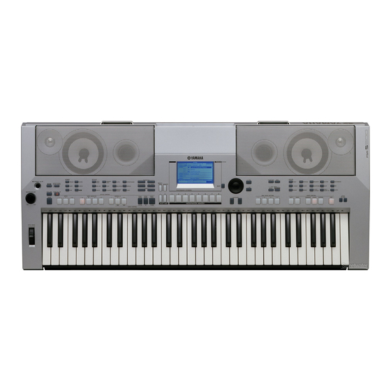
Page 6: Panel Layout(パネルレイアウト
PSR-S500 ■ PANEL LAYOUT(パネルレイアウト) !3 !4 • Front Panel(フロントパネル) q [STANDBY/ON] switch q [電源 切/入](STANDBY/ON)スイッチ w [MASTER VOLUME] control w [全体音量](MASTER VOLUME)コントロール e [DEMO] button e [デモ](DEMO)ボタン r [SONG MODE] button r [ソングモード](SONG MODE)ボタン t SONG t ソング [PRESET], [USER], [USB], [SCOPE] [プリセット](PRESET)、[ユーザー](USER)、... - Page 7 PSR-S500 @2 @3 Rear Panel (リアパネル) Dial ダイアル [+/YES] and [-/NO] buttons [+/YES]、[-/NO]ボタン CATEGORY [ ] and [ ] buttons カテゴリーボタン [ ] 、[ [機能](FUNCTION)ボタン [FUNCTION] button [MDB] button [ミュージックデータベース](MDB)ボタン FILE MENU [MENU] and [EXECUTE] buttons ファイル操作[メニュー](MENU)、[実行] (EXECUTE)ボタン ONE TOUCH SETTING [1] - [4] buttons VOICE ワンタッチセッティング(OTS) [1] - [4]ボタン...
-
Page 8: Circuit Board Layout & Wiring (ユニットレイアウト及び結線図
PSR-S500 ■ CIRCUIT BOARD LAYOUT & WIRING (ユニットレイアウト及び結線図) • Upper Case Assembly( ( ( ( ( 上 上 上 上 上 ケ ケ ケ ケ ケ ー ー ー ー ー ス ス ス ス ス Ass’y) ) ) ) ) JACK W401 •... -
Page 9: Extension Cable For Service Use(サービス用延長ケーブル
PSR-S500 No. Ref. Part No. Assembly Destination Remarks (パーツNo.) (束線) (行き先) (備考) (WH33630) JACK-CN453 SP(WF) WJ465900 FFC4 PNL-CN102 PNR-CN301 WJ466000 FFC5 PNC-CN202 PNL-CN101 WJ465700 FFC2 DM-CN701 PNL-CN103 WJ465800 FFC3 DM-CN901 AM-CN104 (WJ46010) JKAM AM-CN101 JACK-CN451 WJ465600 FFC1 DM-CN501 JACK-CN403 WH336400 AM-CN102 WE138500 DM-CN801... -
Page 10: Disassembly Procedure(分解手順
PSR-S500 ■ DISASSEMBLY PROCEDURE(分解手順) CAUTION: • Be sure to attach the removed filament tape just as it was before removal. • Contacts are visible from the back. Pay attention not to insert and install the cable to the connector inversely. (Fig.1) (注意):... - Page 11 PSR-S500 JACKシート JACK Circuit Board (Time required: About 3 minutes) (所要時間:約3分) Remove the lower case assembly. (See procedure 1.) 下ケースAss'yを外します。 (1項参照) [380A]のネジ5本と[385]のネジ2本を外し、 JACKシー ト を外 Remove the five (5) screws marked [380A] and the two (2) screws marked [385]. The JACK circuit board can します。...
- Page 12 PSR-S500 DMシート DM Circuit Board (所要時間:約4分) (Time required: About 4 minutes) 下ケースAss'yを外します。 (1項参照) Remove the lower case assembly. (See procedure 1.) AMシー ト を外します。 (3項参照) Remove the AM circuit board. (See procedure 3.) [380E]のネジ4本を外し、 DMシー ト を外します。 (図4) Remove the four (4) screws marked [380E]. The DM circuit board can then be removed.
- Page 13 PSR-S500 PSWシート PSW Circuit Board (Time required: About 3 minutes) (所要時間:約3分) Remove the lower case assembly. (See procedure 1.) 下ケースAss'yを外します。 (1項参照) [380C]のネジ2本を外し、 PSWシー ト を外します。 (図3) Remove the two (2) screws marked [380C]. The PSW circuit board can then be removed. (Fig.3) PSWシー...
- Page 14 PSR-S500 PNC Circuit Board PNCシート (Time required: About 6 minutes) (所要時間:約6分) 9-7-1 Remove the AM circuit board. (See procedure 3.) 9-7-1 AMシー ト を外します。 (3項参照) 9-7-2 Remove the DM circuit board. (See procedure 4.) 9-7-2 DMシー ト を外します。 (4項参照) 9-7-3 Remove the ten (10) screws marked [380J]. The PNC 9-7-3 [380J]のネジ10本を外し、...
- Page 15 PSR-S500 Rubber Contact 12P Rubber Contact 12P Rubber Contact 13P (接点ゴム 12P) (接点ゴム 12P) (接点ゴム 13P) [180A] [180B] [190B] [190A] Lower Key Bed Assembly Keyboard Assembly (下ケース鍵盤Ass'y) (16N-C61鍵盤Ass'y) [200A] [200A] [200A] [200A] [200B] [200A] B2 C3 B3 C4 B4 C5 B5 C6 One octave One octave...
- Page 16 PSR-S500 When installing the 61L circuit board (MK-L), tighten * * * * * シ シ シ シ シ ー ー ー ー ー ト ト ト ト ト 6 1 L 6 1 L 6 1 L 6 1 L 6 1 L (...
-
Page 17: Lsi Pin Description(Lsi 端子機能表
PSR-S500 ■ LSI PIN DESCRIPTION(LSI 端子機能表) CONTENTS(目次) ● ISP1161A1BD (X5879A00) USB CONTOLLER ............17 YMW767-VTZ (X6055A00) CPU+XG ................18 ● ● MB87S1280 (X6363A00) SSP1 ................... 19 µ ● PD789022GB-A15-8E (XZ560100) CPU ..............20 ● MN101C027YB (XS711200) CPU ................20 ● PCM1753DBQR (X7889A00) DAC ................ - Page 18 PSR-S500 YMW767-VTZ (X6055A00) CPU+XG DM: IC101 NAME FUNCTION NAME FUNCTION TESTN Input for TEST IOVDD IOVDD +3.3V PLLBPN PLL bypass select LBN/LWRN/PF6 External memory lower-byte enable PLLVDD PLLVDD +2.5V UBN/UWRN/PF7 External memory upper-byte enable Capacitor terminal for PLL RDN/PF4 External memory read enable PLLVSS PLLVSS MD00...
- Page 19 PSR-S500 MB87S1280 (X6363A00) SSP1 DM:IC401 NAME FUNCTION NAME FUNCTION WAITN Wait for external CPU MD[7] Data bus(ARM,DSP -> memory) IRQN_OUT Output of interrupt information MD[6] Data bus(ARM,DSP -> memory) VDDE VDDE +3.3V MD[5] SCANSW[4] MD[4] SCANSW[3] MD[3] Data bus(ARM,DSP -> memory) SCANSW[2] Scan control MD[2]...
- Page 20 PSR-S500 µPD789022GB-A15-8E (XZ560100) CPU DM:IC801 NAME FUNCTION NAME FUNCTION P32/INTP2/CPT2 Port 3/External interrupt input/Capture edge input Port 1 P31/INTP1 Port 3/External interrupt input P30/INTP0 P47/KR7 P22/RXD/SI0 Port 2/Asynchronous serial interface serial data input/Serial interface serial data input P46/KR6 P21/TXD/SO0 Port 2/Asynchronous serial interface serial data output/Serial interface serial data output P45/KR5 P20/ASCK//SCK0 Port 2/Asynchronous serial interface serial clock input/Serial interface serial clock...
- Page 21 PSR-S500 S1D13700F01A100 (X5422A00) LCD CONTROLLER DM:IC601 NAME FUNCTION NAME FUNCTION – Ground – Ground AB12 XCD1 Drain output AB11 XCG1 Gate input AB10 Adorress bus RESET# Reset SCANEN Test mode set up input TESTEN HIOVDD – Power supply CLKI Externally sourced system clock COREVDD –...
-
Page 22: Ic Block Diagram(Ic ブロック図
PSR-S500 ■ IC BLOCK DIAGRAM(IC ブロック図) SN74LVC138APWR(X7074A00) SN74LV32APWR (X5647A00) NJM4580E(TE2) (X2331A00) RC4580IDR (X7419A00) 3 to 8 Demultiplexer Quad 2 Input OR DM: IC302 DM:IC304, IC311 Dual Operational Amplifier DM: IC203 +DC Voltage Output A Supply Select Inverting Output B Input A Inverting Non-Inverting Input A... -
Page 23: Circuit Boards(シート基板図
PSR-S500 ■ CIRCUIT BOARDS(シート基板図) CONTENTS(目次) ● 61H Circuit Board (X2335C0) ..................34 ● 61L Circuit Board (X2336B0) ..................34 ● AM Circuit Board (X7722C0) ..................26 DM Circuit Board (X7721D0) ..................24 ● ● ENC Circuit Board (X7722C0) ..................27 ●... - Page 24 PSR-S500 DM Circuit Board ● to PNL-CN103 to LCD Unit to AM-CN104 to 61L-CN5 to 61H-CN1 to 61H-CN2 to ENC-CN301 Component Side(部品側) to JACK-CN403 Not installed 2NA-WH33370 Note: See parts list for details of circuit board component parts. 注:シートの部品詳細はパーツリストをご参照ください。...
- Page 25 PSR-S500 DM Circuit Board ● Pattern Side(パターン側) 2NA-WH33370...
- Page 26 PSR-S500 AM Circuit Board ● MVR Circuit Board ● to AM-CN204 to LCD Backlight MASTER VOLUME Component Side(部品側) PB Circuit Board ● PITCH BEND to AM-CN103 Component Side(部品側) Component Side(部品側) 2NA-WH33410 MVR: 2NA-WH33410 Note: See parts list for details of circuit board component parts. 2NA-WH33410 注:シートの部品詳細はパーツリストをご参照ください。...
- Page 27 PSR-S500 JACK Circuit Board ● PSW Circuit Board ● to JACK-CN452 STANDBY/ON Component Side(部品側) ENC Circuit Board ● to DM-CN702 Rotary Encoder Component Side(部品側) TW Circuit Board ● TWL: to Tweeter L(ツィーター(左)) TWL: to Tweeter R(ツィーター(右)) TWL: to JACK-CN455 TWR: to JACK-CN454 Component Side(部品側)...
- Page 28 PSR-S500 PNL Circuit Board ● Component Side(部品側) Note: See parts list for details of circuit board component parts. 2NA-WH33400 注:シートの部品詳細はパーツリストをご参照ください。...
- Page 29 PSR-S500 PNL Circuit Board ● to PNC-CN202 to PNR-CN301 to DM-CN701 Pattern Side(パターン側) 2NA-WH33400...
- Page 30 PSR-S500 PNC Circuit Board ● Component Side(部品側) 2NA-WH50940 Note: See parts list for details of circuit board component parts. 注:シートの部品詳細はパーツリストをご参照ください。...
- Page 31 PSR-S500 PNC Circuit Board ● to PNL-CN101 Pattern Side(パターン側) 2NA-WH50940...
- Page 32 PSR-S500 PNR Circuit Board ● Component Side(部品側) Note: See parts list for details of circuit board component parts. 2NA-WH50940 注:シートの部品詳細はパーツリストをご参照ください。...
- Page 33 PSR-S500 PNR Circuit Board ● to PNL-CN102 Pattern Side(パターン側) 2NA-WH50940...
- Page 34 PSR-S500 61H Circuit Board to DM-CN801 to 61L-CN4 to DM-CN803 61L Circuit Board to DM-CN802 to 61H-CN3 61H: 2NAKB-V869540 Note: See parts list for details of circuit board component parts. 61L: 2NAKB-V869520 注:シートの部品詳細はパーツリストをご参照ください。...
-
Page 35: Test Program
3) Jigs: Foot switch (FC-4 or FC-5), USB cable, USB memory, USB-MIDI driver (*1) PC (Install a USB-MIDI driver (*1) in PC and finish the THROUGH setup.) *1 Obtain the USB-MIDI driver from CD-ROM(X7838A00) for PSR-S500 or Yamaha official website. (URL>>http://www.yamahapkclub.com) HOW TO ENTER THE TEST PROGRAM While pressing the C2#, F2 and G2# keys, turn the [STANDBY/ON] switch on. - Page 36 PSR-S500 D. Test Item List TEST LCD Display Test Descriptions, Judgment Criteria 003 Ram Chk1 Checks the RAM that is connected to the CPU bus. The test results appear on the LCD. Check that the LCD displays "Main/Sub/SSP1 OK". (OK:"Main/Sub/SSP1 OK", NG:"Main/Sub/SSP1 NG") 006 Flash Rom Chk1 Checks the flash ROM that is connected to CPU bus.
- Page 37 PSR-S500 TEST LCD Display Test Descriptions, Judgment Criteria 028 LCD On Check that all LCD dots are on. (The whole screen becomes white.) 029 LCD Off Check that all LCD dots are off. (The whole screen becomes blue.) 031 Pedal1 Chk Connect the foot switch (FC-4 or FC-5) to the [SUSTAIN] jack.
- Page 38 PSR-S500 ■ テストプログラム ※ テストナンバー47のFactory Setを実行すると、設定したデータが失われます。 事前にユーザーデータをバックアップしておいて下さい。 測定条件 1) AC アダプターは PA-300、PA-301 を使用します。 2) 測定器: 周波数カウンター、レベル計(JIS-C フィルター使用) 注) 特に指示のない限りステレオプラグを用い、33 Ω負荷を接続して[PHONES/OUTPUT]端子にて測定します。 3) 治具:フットスイッチ(FC-4 または FC-5) 、USB ケーブル、USB メモリー、USB-MIDI ドライバー(*1) PC(USB-MIDI ドライバー(*1)をインストールし、PC 側は[Thru On]に設定しておきます。) PSR-S500 に付属の CD-ROM(X7838A00)又はヤマハホームページのダウンロードページから入手して下さい。 (URL>>http://www.yamahapkclub.com) テストプログラムの起動 C2# と F2 と G2# を同時に鍵盤を押さえながら、 [電源]スイッチを ON にします。 テストの進め方...
- Page 39 PSR-S500 テスト一覧 テスト LCD 表示 テスト内容及び判定条件 -- コントラストボリュームチェック。 LCD の視認しやすい位置にコントラストボリュームを設定します。 右回りで青、左回りで白くなります。 001 Version バージョン表示 ROM(Prog,Data,Wave,SSP1)のバージョンを表示します。 (OK の場合:"XXX" Prog/Data/Wave/SSP1, NG の場合:"Err" Prog/Data/Wave/SSP1) 002 Rom Chk1 ROM チェック CPU のバスに接続されている ROM をチェックします。 チェックの結果が LCD に表示されます。 (OK の場合:Prog/Data/Wave/SSP1 OK, NG の場合:Prog/Data/Wave/SSP1 NG) 003 Ram Chk1 RAM チェック...
- Page 40 PSR-S500 テスト LCD 表示 テスト内容及び判定条件 021 All LED Chk パネル LED 全点灯チェック パネルの全ての LED が点灯することを確認します。 022 Red LED Chk パネル赤色 LED 全点灯チェック パネルの全ての赤色 LED が点灯することを確認します。 023 Green LED Chk パネル緑色 LED 全点灯チェック パネルの全ての緑色 LED が点灯することを確認します。 028 LCD On LCD 全点灯チェック LCD の全てのドットが点灯することを確認します。...
- Page 41 PSR-S500 Table 1(表1) ORDER SWITCH NAME NOTE ORDER SWITCH NAME NOTE (順番) (SW名) (ノート番号) (順番) (SW名) (ノート番号) DIAL UP DIAL DOWN ORGAN DEMO BRASS SONG MODE FLUTE SONG PRESET PERCUSSION SONG SCORE SYNTH SONG USER OTS LINK SONG LYRICS AUTO FILL IN SONG USB ACMP SONG REC...
-
Page 42: Initialization(初期化
PSR-S500 ■ INITIALIZATION This function erases all backup data in the instrument's internal memory and restores the initial default settings and data. The following initialization procedures are provided. Backup Clear To clear data backed up to the internal memory, simultaneously hold the highest white key on the keyboard and turn the power on by pressing the [STANDBY/ON] switch. - Page 43 PSR-S500 ■ 初期化 この楽器の内部メモリーにあるソングデータやバックアップデータを消去し、設定を初期設定 (工場出荷時の状態)に戻すことを「初期化」と呼びます。初期化は以下の方法で行なってください。 バックアップクリア 本体のバックアップデータをクリアしたいときは、鍵盤の最高音(白鍵)を押しながら [電源切/入](STANDBY/ON)スイッチを押して電源を入れると、上記のデータは消去 され、楽器は初期設定値に戻ります。 メモリクリア コンピューターから本体内部メモリーに転送したソングデータやスタイルファイルをク リアしたいときは、鍵盤の最高音(白鍵)と一番高い黒鍵3つを同時に押しながら[電源 切/入](STANDBY/ON)スイッチを押して電源を入れると、上記のデータは消去されま す。 フラッシュクリアすると、購入した有料のソングデータも消去されます。消去したく ないデータは、必要に応じてコンピューターに保存して下さい。...
-
Page 44: Data Backup
PSR-S500 ■ DATA BACKUP To backup user data to an external device, use a USB flash memory. Refer to the following for the data you can backup using it. * User Songs * Style Files * Registration Memory Data * Auto Fill In On/Off * Each parameters in the function display: Timing, Split point, Touch sensitivity, Style volume, Metronome volume, Demo cancel, Language Master EQ type, Chrd fingering... -
Page 45: Formatting Usb Flash Memory
PSR-S500 Formatting USB Flash Memory A new USB flash memory device must be formatted before it can be used by this instrument. CAUTION Press the [EXECUTE] button again, or the • If you format a USB flash memory that already contains data, all of the data will be erased. - Page 46 PSR-S500 Saving Data Three types of data are saved to one “User File” by this operation: user song, style file, and registration memory data. When you save a “User File” the style file and registration memory are also saved automatically. Make sure that a appropriately formatted USB flash memory device has been properly connected to the instrument’s USB TO...
-
Page 47: Loading User Files And Style Files
PSR-S500 Loading User Files and Style Files User files and style file residing on a USB flash memory can be loaded to the instrument. Use the dial to select the user file or style CAUTION file you want to load. •... - Page 48 PSR-S500 ■ ユーザーデータのバックアップ ユーザーデータを外部機器へバックアップする際は、USBフラッシュメモリーをご利用下さい。 バックアップ可能なデータについては下記をご参照ください。 • ユーザーソング • スタイルファイル • レジストレーションメモリー • 自動フィルイン オン/オフ • FUNCTION画面内の各設定:チューニング、スプリットポイント、タッチ感度、スタイル音量、ソング音量、 メトロノーム音量、デモキャンセル、言語切り替え、マスターEQタイプ、 コードフィンガリング USBフラッシュメモリーを接続する USBフラッシュメモリーを USB TO DEVICE MAIN画面右下のUSBアクセス表示に 端子に、正しい向きで接続してください [CONNECT]と表示されているか確認します USBフラッシュメモリーの向き(上下、前後)を間違えない ようご注意ください。 CONNECT この状態で[メニュー](MENU)ボタンを押すと、USBフラ ッシュメモリーの操作ができる FILE CONTROL (ファイ ルコントロール)画面に入ります。ただし、この段階では まだ押さないでください。 IMPORTANT NOTE • コンピューターなど他の機器からUSBフラッシュメモリーにコピ •...
- Page 49 PSR-S500 USBフラッシュメモリーのフォーマット 市販のUSBフラッシュメモリーを、この楽器で使用できる状態にすることをフォーマット(初期化)といいます。 [実行](EXECUTE)ボタンを押すと、フォーマッ トの実行を再確認する表示が表れます • データが入っているUSBフラッシュメモリーをフォーマットすると キャンセルする場合は、[−/NO]ボタンを押します。 、中に記録されていたデータはすべて失われてしまいます。大切な データをフォーマットで消してしまわないようにご注意ください。 [実行](EXECUTE)ボタン又は[+/YES]ボタ ンを押すと、フォーマットが実行されます。 フォーマットするUSBフラッシュメモリーが USB TO DEVICE端子に接続された状態で、 MAIN 画面右下のUSBアクセス表示に • フォーマット実行中はキャンセルできません。絶対に電源を切 [CONNECT]と表示されているのを確認してく ったりUSBフラッシュメモリーを抜いたりしないでください。 ださい ファイルコントロールの[メニュー](MENU)ボ フォーマットが完了すると、メッセージが表示 タンを押して、FILE CONTROL 画面の Format されます の項目を表示させます [画面戻る](EXIT)ボタンを押してMAIN画面へ戻ります。 ファイル操作 NOTE 実行 メニュー • USBフラッシュメモリーにライトプロテクトがかかってい る場合はメッセージが表示され、フォーマット操作はでき ません。 カテゴリーボタン[ ]、[ ]を何度か押して、...
- Page 50 PSR-S500 ユーザーファイルを保存する ここで保存するユーザーファイルとは、ユーザーソング、スタイルファイル、レジストレーションメモリーの3つです。 これらは1つのファイルとして保存されます。 フォーマット済みのUSBフラッシュメモリー が USB TO DEVICE端子に接続された状態で 、MAIN 画面右下のUSBアクセス表示に [CONNECT]と表示されているのを確認して ください ファイル操作の[メニュー](MENU)ボタンを押 します カーソルを カーソルを 文字消去 ダイアルで カテゴリーボタン[ ]、[ ]を何度か押して、 左へ移動 右へ移動 文字を選択 ユーザーファイルセーブの項目「User File Save」を表示させます 保存操作によって作成されるファイルの名前が自動的に 付けられます。 カテゴリー カーソル [実行](EXECUTE)ボタンを押します。保存の 実行を確認する画面が表示されます キャンセルする場合は[−/NO]ボタンを押します。 ●すでにあるファイルを書き替えるには すでにUSBフラッシュメモリーにあるユーザー [実行](EXECUTE)ボタンまたは[+/YES]ボタ データファイルに上書きをする(書き替える)場合 ンを押すと保存が実行されます は、ダイアルや[+]、[−]ボタンでファイルを選...
- Page 51 PSR-S500 ユーザーファイルやスタイルファイルを読み込む(ロード) USBフラッシュメモリー内のユーザーファイルやスタイルファイルを、本体メモリーに読み込みます。 ダイアルを回して、読み込みたいユーザーフ ァイルまたはスタイルファイルを選択します • ユーザーファイルを読み込むと、001∼005のユーザーソング、ス USBフラッシュメモリー内にあるユーザーファイルがす タイルファイル(ユーザースタイル)、レジストレーションメモリ べて表示されると、次にスタイルファイルが表示されま ーはすべて上書きされます。スタイルファイルだけを読み込んだ す。 場合は、スタイルファイルだけ上書きされます。大切なデータは 読み込み前にUSBフラッシュメモリーに保存しておいて下さい。 NOTE • スタイルファイルは、USBフラッシュメモリーのルートにあ る必要があります。フォルダー内にあるスタイルファイルは 読み込みたいファイルの入ったUSBフラッシ 認識されません。 ュメモリーが USB TO DEVICE端子に接続され た状態で、MAIN 画面右下のUSBアクセス表示 [実行](EXECUTE)ボタンを押します。読み込 に[CONNECT]と表示されているのを確認して みの実行を確認する画面が表示されます ください キャンセルする場合は[−]ボタンを押します。 ファイルコントロールの[メニュー](MENU)ボ タンを押します [実行](EXECUTE)ボタンまたは[+/YES]ボタ ンを押すと読み込みが実行されます カテゴリーボタン[ ]、[ ]を何度か押してロ ードの項目「Load」を表示させます • 読み込み中はキャンセルできません。絶対に電源を切ったりUSB カテゴリー...
-
Page 52: System Booting Flow Chart
MIDI. reach this stage. The LCD or the LCDC IC is Backup NG ? The Yamaha logo display defective, if the LCD does not Displays the Flash ROM is defective (Opening screen) display the Yamaha logo. -
Page 53: システム起動フローチャート
PSR-S500 ■ システム起動フローチャート Power On 各種レジスタ設定 ポートの初期化 非バックアップ 変数の初期設定 FLASH/WE = L 各タスクの初期化 /MKS_IC = L ※SSP1への通信 MKS_ACK = H はこの辺りから。 DM シート /LCD_IC = L FLASH/WE: IC101 126,127pin LCD_DISP = L シリアル通信開始 /MKS_IC: IC101 29pin A/D_SEL = L MKS_ACK: IC101 37pin (PANEL) /PANEL_IC = L /LCD_IC:... -
Page 54: Midi Implementation Chart(Midi インプリメンテーションチャート
PSR-S500 ■ MIDI IMPLEMENTATION CHART(MIDI インプリメンテーションチャート) YAMAHA [ Portable Keyboard ] Date:18-Jul-2006 Model PSR-S500 MIDI Implementation Chart Version:1.0 Transmitted Recognized Remarks Function... Basic Default 1 - 16 1 - 16 Channel Changed Default Mode Messages Altered ************** Note 0 - 127... -
Page 55: Midi Dataformat
PSR-S500 ■ MIDI DATAFORMAT NOTE: 1 By default (factory settings) the instrument ordinarily functions <Reverb Type> F0H, 43H, 1nH, 4CH, 02H, 01H, 00H, mmH, as a 16-channel multi-timbral tone generator, and incoming llH, F7H data does not affect the panel voices or panel settings. How- •... - Page 56 PSR-S500 Chorus Types Type Description CHORUS1 CHORUS2 CHORUS3 CHORUS4 CHORUS5 CHORUS6 CHORUS7 Conventional chorus program with rich, warm chorusing. CHORUS8 GM CHORUS1 GM CHORUS2 GM CHORUS3 GM CHORUS4 FB CHORUS CELESTE1 A 3-phase LFO adds modulation and spaciousness to the sound. CELESTE2 FLANGER1 FLANGER2...
- Page 57 PSR-S500 Type Description SYMPHONIC1 Adds more stages to the modulation of Celeste. SYMPHONIC2 ENS DETUNE Chorus effect without modulation, created by adding a slightly pitch-shifted sound. KARAOKE1 KARAOKE2 Echo for karaoke. KARAOKE3 This effect isolates only the early reflection components of the reverb. GATE REVERB Simulation of gated reverb.
- Page 58 PSR-S500 Type Description PHASER1 PHASER2 EP PHASER1 Cyclically modulates the phase to add modulation to the sound. EP PHASER2 EP PHASER3 DYN PHASER PITCH CHG1 PITCH CHG2 Changes the pitch of the input signal. PITCH CHG3 ROTARY SP1 ROTARY SP2 ROTARY SP3 ROTARY SP4 ROTARY SP5...
-
Page 59: Parts List
PARTS LIST CONTENTS(目次) OVERALL ASSEMBLY (総組立) ..........2 UPPER CASE ASSEMBLY(上ケースAss’y) ......4 KEYBOARD ASSEMBLY (GH3 鍵盤 Ass’y ) ......7 LOWER CASE ASSEMBLY(下ケースAss’y) ......8 ELECTRICAL PARTS(電気部品) .......... 10 Note) DESTINATION ABBREVIATIONS Australian model Chinese model British model South-east Asia model Canadian model Taiwan model German model... - Page 60 PSR-S500 ■ OVERALL ASSEMBLY (総組立) Upper case assembly Music rest See page 4. (譜面板) (上ケースAss'y) (4ページ参照) Lower case assembly See page 8. (下ケースAss'y) (8ページ参照) Lower key bed assembly (下ケース鍵盤Ass'y) Keyboard assembly See page 7. (16N-C61鍵盤) (7ページ参照) L110 AC adaptor(PA-301) (ACアダプター(PA-301)) This figure shows Japanese model.
- Page 61 PSR-S500 PART NO. DESCRIPTION 部 品 名 REMARKS REF NO. QTY RANK OVERALL ASSEMBLY 総 組 立 PSR-S500 Overall Assembly 総 組 立 (WH03840) Upper Case Assembly 上 ケ ー ス A s s ’ y (WH08850) Lower Key Bed Assembly 下...
- Page 62 PSR-S500 ■ UPPER CASE ASSEMBLY (上ケース Ass’y) 385 450 310b 310a...
- Page 63 PSR-S500 PART NO. DESCRIPTION 部 品 名 REMARKS REF NO. QTY RANK UPPER CASE ASSEMBLY 上 ケ ー ス A s s ’ y PSR-S500 Upper Case Assembly 上 ケ ー ス A s s ’ y (WH08850) WH038500 Upper Case 上...
- Page 64 PSR-S500 PART NO. DESCRIPTION 部 品 名 REMARKS REF NO. QTY RANK Wiring Assembly JKAM J K A M 束 線 A s s ’ y (WJ46010) WJ465600 Wiring Assembly FFC1 F F C 束 線 1 WH336400 Connector Assembly LCD L...
- Page 65 PSR-S500 ■ KEYBOARD ASSEMBLY (16N-C61 鍵盤 Ass’y ) Keyboard assembly (16N-C61鍵盤) MK circuit board assembly (MKシートAss'y) Lower case F (下ケース成形品(F)) 部 品 名 PART NO. DESCRIPTION REMARKS REF NO. QTY RANK KEYBOARD ASSEMBLY 1 6 N − C 6 1 鍵 盤 PSR-S500 Keyboard Assembly 1...
- Page 66 PSR-S500 ■ LOWER CASE ASSEMBLY (下ケース Ass’y) L20b L20a L30b L30a Lower case sub assembly (下ケースサブAss'y)
- Page 67 PSR-S500 PART NO. DESCRIPTION 部 品 名 REMARKS REF NO. QTY RANK LOWER CASE ASSEMBLY 下 ケ ー ス A s s ’ y PSR-S500 Lower Case Assembly 下 ケ ー ス A s s ’ y (WH08870) WH088800 Lower Case Sub Assembly 下...
- Page 68 PSR-S500 ■ ELECTRICAL PARTS(電気部品) PART NO. DESCRIPTION 部 品 名 REMARKS REF NO. QTY RANK ELECTRICAL PARTS 電 気 部 品 PSR-S500 WH334300 Circuit Board A M シ ー ト (WH33410)(X7722C0) WH334500 Circuit Board E N C シ ー ト (WH33410)(X7722C0) WH334200 Circuit Board...
- Page 69 PSR-S500 PART NO. DESCRIPTION 部 品 名 REMARKS REF NO. QTY RANK V5515400 Mylar Capacitor C214 0.1000 50V J マ イ ラ ー コ ン VR168300 C214 Monolithic Mylar Capacitor ECQ-V1H104JL3 積 層 マ イ ラ ー コ ン UA355100 Mylar Capacitor マ...
- Page 70 PSR-S500 PART NO. DESCRIPTION 部 品 名 REMARKS REF NO. QTY RANK VT279200 Coil L405 DX001-20UH TATEJI コ イ ル 2 0 U 天 津 VB835000 Coil L406 FL05RD200AT TATETE コ イ ル 2 0 U VT279200 Coil L406 DX001-20UH TATEJI...
- Page 71 PSR-S500 PART NO. DESCRIPTION 部 品 名 REMARKS REF NO. QTY RANK US145100 Ceramic Capacitor-F (chip) -318 0.1000 25V Z RECT. チ ッ プ セ ラ ( F ) UF118470 Electrolytic Cap. (chip) C401 470 6.3V UUR0J4 チ ッ プ ケ ミ コ ン UF038100 Electrolytic Cap.
- Page 72 PSR-S500 PART NO. DESCRIPTION 部 品 名 REMARKS REF NO. QTY RANK US145100 Ceramic Capacitor-F (chip) -907 0.1000 25V Z RECT. チ ッ プ セ ラ ( F ) US145100 C909 Ceramic Capacitor-F (chip) 0.1000 25V Z RECT. チ ッ プ セ ラ ( F ) US145100 Ceramic Capacitor-F (chip) チ...
- Page 73 PSR-S500 PART NO. DESCRIPTION 部 品 名 REMARKS REF NO. QTY RANK WH469300 Common Mode Coil L501 DLP31SN121ML2L コ モ ン モ ー ド コ イ ル WH469300 Common Mode Coil L502 DLP31SN121ML2L コ モ ン モ ー ド コ イ ル V8589700 Chip Inductance L601...
- Page 74 PSR-S500 PART NO. DESCRIPTION 部 品 名 REMARKS REF NO. QTY RANK RD356100 Carbon Resistor (chip) R617 1.0K 63M J RECT. チ ッ プ 抵 抗 RD353100 Carbon Resistor (chip) R618 1.0 63M J RECT. チ ッ プ 抵 抗 RD353100 Carbon Resistor (chip) -620...
- Page 75 PSR-S500 PART NO. DESCRIPTION 部 品 名 REMARKS REF NO. QTY RANK WF300900 LED (chip) LD109 SML-512DW ORANGE チ ッ プ L E D テ ー ENDING 1 WF300900 LD110 LED (chip) SML-512DW ORANGE チ ッ プ L E D テ ー ENDING 2 WF300900 LED (chip)
- Page 76 PSR-S500 PART NO. DESCRIPTION 部 品 名 REMARKS REF NO. QTY RANK WF300900 LED (chip) LD207 SML-512DW ORANGE チ ッ プ L E D テ ー MEMORY 4 WF301000 LED (chip) LD208 SML-012PTT86A GREE チ ッ プ L E D テ ー MEMORY 4 WF300900 LED (chip)
- Page 77 < Page1 > PSR-S500 PSR-S500 OVERALL CIRCUIT DIAGRAM 1/6 (DM 1/3 ) Reset Time: 50mS Detect Voltage: 3.6V <Page2 E4> <Page2 G2> RESET <Page2 E6> <Page3 D3> <Page2 D7> CPU+XG <Page2 C3> <Page3 D2> <Page3 H3> P2ROM P2ROM P2ROM (WAVE) (PROG, WAVE) (WAVE) <Page2 I7>...
- Page 78 < Page2 > PSR-S500 PSR-S500 OVERALL CIRCUIT DIAGRAM 2/6 (DM 2/3, JACK 2/2 ) JACK SUSTAIN P2ROM(PROG) TO HOST <Page3 D4> W401 <Page1 C2> not installed <Page3 E5> <Page3 I7> <Page1 D4> TO DEVICE SSP1 <Page1 C3> CONTRAST DRAM (4M) 28CC1-2001009321-2 2 DC/DC CONVERTER USB HIGH SIDE SWITCH...
- Page 79 < Page3 > PSR-S500 PSR-S500 OVERALL CIRCUIT DIAGRAM 3/6 (DM 3/3 ) <Page1 B3> <Page1 C3> to PNL-CN103 <Page6 K5> <Page1 C3> to 61H-CN1 <Page1 B4> <Page5 C5> to ENC-CN301 not installed <Page1 B3> <Page4 B6> <Page1 B3> not installed to 61L-CN5 <Page5 C8>...
- Page 80 < Page4 > PSR-S500 PSR-S500 OVERALL CIRCUIT DIAGRAM 4/6 (AM, ENC, JACK 1/2, MVR, PB, PSW, TW ) JACK POWER AMP PHONES/ 28CC1-2001009321-1 2 OUTPUT to DM-CN901 <Page3 J6> DCIN 16V DC/DC CONVERTER 28CC1-2001009321-1 2 PITCH BEND 28CC1-2001009321-1 2 REGULATOR +5V LCD Back Light 28CC1-2001009321-1 2 28CC1-2001009321-1 2...
- Page 81 < Page5 > PSR-S500 PSR-S500 OVERALL CIRCUIT DIAGRAM 5/6 (PNC, PNR, 61H, 61L) to PNL-CN101 <Page6 K2> to PNL-CN102 <Page6 K4> 28CC1-2001009323-2 28CC1-2001009323-1 1 to DM-CN801 (C4~C6) <Page3 J3> to DM-CN803 <Page3 J5> 28CC1-8822437 (C1~B3) to DM-CN802 <Page3 J4> 28CC1-8822436 WARNING Components having special characteristics are maked and must be replaced...
- Page 82 < Page6 > PSR-S500 PSR-S500 OVERALL CIRCUIT DIAGRAM 6/6 (PNL ) to PNC-CN202 <Page5 A2> to PNR-CN301 <Page5 F3> to DM-CN701 <Page3 B2> 28CC1-2001009322 1 (セ):Ceramic Capacitor(セラミックコンデンサー) WARNING Components having special characteristics are maked and must be replaced with parts having specification equal to those originally installed. Note: See parts list for details of circuit board component parts.