Table of Contents
Advertisement
Quick Links
Advertisement
Table of Contents

Related Manuals for Clevo N240BU


Summary of Contents for Clevo N240BU
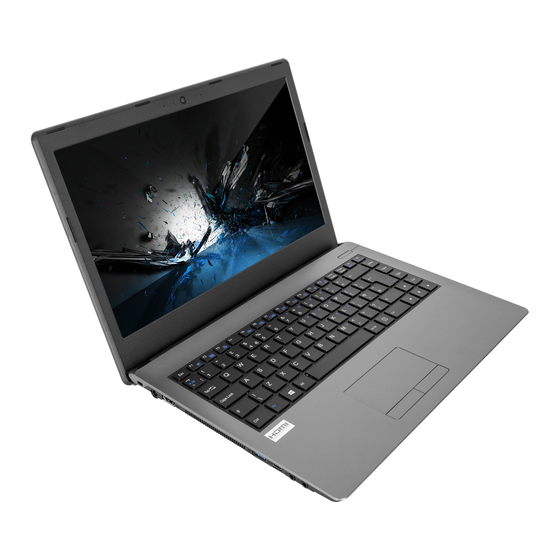
- Page 1 N240BU / N241BU...
- Page 3 Preface Notebook Computer N240BU / N241BU Service Manual...
- Page 4 Preface Notice The company reserves the right to revise this publication or to change its contents without notice. Information contained herein is for reference only and does not constitute a commitment on the part of the manufacturer or any subsequent ven- dor.
- Page 5 This manual is intended for service personnel who have completed sufficient training to undertake the maintenance and inspection of personal computers. It is organized to allow you to look up basic information for servicing and/or upgrading components of the N240BU / N241BU series notebook PC.
- Page 6 Preface IMPORTANT SAFETY INSTRUCTIONS Follow basic safety precautions, including those listed below, to reduce the risk of fire, electric shock and injury to per- sons when using any electrical equipment: 1. Do not use this product near water, for example near a bath tub, wash bowl, kitchen sink or laundry tub, in a wet basement or near a swimming pool.
-
Page 7: Instructions For Care And Operation
Preface Instructions for Care and Operation The notebook computer is quite rugged, but it can be damaged. To prevent this, follow these suggestions: Don’t drop it, or expose it to shock. If the computer falls, the case and the components could be damaged. Do not expose the computer Do not place it on an unstable Do not place anything heavy... -
Page 8: Power Safety
Preface Avoid interference. Keep the computer away from high capacity transformers, electric motors, and other strong mag- netic fields. These can hinder proper performance and damage your data. Take care when using peripheral devices. Use only approved brands of Unplug the power cord before peripherals. -
Page 9: Battery Precautions
Preface Battery Precautions • Only use batteries designed for this computer. The wrong battery type may explode, leak or damage the computer. • Do not continue to use a battery that has been dropped, or that appears damaged (e.g. bent or twisted) in any way. Even if the computer continues to work with a damaged battery in place, it may cause circuit damage, which may possibly result in fire. - Page 10 Preface Related Documents You may also need to consult the following manual for additional information: User’s Manual on CD/DVD This describes the notebook PC’s features and the procedures for operating the computer and its ROM-based setup pro- gram. It also describes the installation and operation of the utility programs provided with the notebook PC. System Startup °...
-
Page 11: Table Of Contents
Preface Contents Introduction ..........1-1 Bottom ................... A-4 LCD ....................A-5 Overview ..................1-1 HDD ....................A-6 Specifications ..................1-2 Schematic Diagrams......... B-1 External Locator - Top View with LCD Panel Open ......1-4 External Locator - Front & Right Side Views .........1-5 System Block Diagram ..............B-2 External Locator - Left Side &... - Page 12 Preface 3V, 5V, 3VS, 5VS, CTL Signal ........... B-28 VDD3, VDD5 ................B-29 VDDQ_VTT, 1.5VS, 1.8VS ............B-30 1.0V Series ................... B-31 VCore, VCCGT, VCCSA, VCCIO ..........B-32 RT3601BC ................... B-33 Charger, DC-In ................B-34 USB Board ................... B-35 CRT ....................B-36 RTL8411B ..................
-
Page 13: Introduction
Chapter 1: Introduction Overview This manual covers the information you need to service or upgrade the N240BU / N241BU series notebook computer. Information about operating the computer (e.g. getting started, and the Setup utility) is in the User’s Manual. Information about dri-vers (e.g. -
Page 14: Specifications
Introduction Specifications Processor Options Storage Intel® Core™ i7 Processor One Changeable 2.5" 7mm (h) SATA HDD/SSD i7-7500U (2.70GHz) (Factory Option) One M.2 SATA/PCIe Gen3 x4 Solid State 4MB Smart Cache, 14nm, DDR4-2133MHz, TDP 15W Drive (SSD) Intel® Core™ i5 Processor Latest Specification Information Pointing Device i5-7200U (2.50GHz) - Page 15 Introduction Interface Environmental Spec One USB 2.0 Port Temperature ° ° One USB 3.0 (USB 3.1 Gen 1) Port Operating: 5 C - 35 One USB 3.0 (USB 3.1 Gen 1) Type C Port Or Non-Operating: -20°C - 60°C (Factory Option) One USB 3.1 Gen 2 Type C Port Relative Humidity One HDMI-Out Port Operating: 20% - 80%...
-
Page 16: External Locator - Top View With Lcd Panel Open
Introduction External Locator - Top View with LCD Panel Open Figure 1 Top View 1. PC Camera 2. *PC Camera LED *When the PC camera is in use, the LED will be illuminated in red. 3. Built-In Microphone 4. LCD 5. -
Page 17: External Locator - Front & Right Side Views
Introduction External Locator - Front & Right Side Views Figure 2 Front View 1. LED Indicator FRONT VIEW Figure 3 Right Side View 1. USB 2.0 Port RIGHT SIDE VIEW 2. Multi-in-1 Card Reader 3. External Monitor Port 4. RJ-45 LAN Jack External Locator - Front &... -
Page 18: External Locator - Left Side & Rear View
Introduction External Locator - Left Side & Rear View Figure 4 Left Side View 1. Security Lock Slot 2. DC-In Jack 3. HDMI-Out Port LEFT SIDE VIEW 4. Vent 5. USB 3.0/3.1 Port 6. USB 3.0/3.1 Type C Port 7. Microphone-In Jack 8. -
Page 19: External Locator - Bottom View
Introduction External Locator - Bottom View Figure 6 Bottom View 1. Battery 2. Vent 3. Speakers Overheating To prevent your com- puter from overhea- ting, make sure no- thing blocks any vent while the computer is in use. External Locator - Bottom View 1 - 7... -
Page 20: Mainboard Overview - Top (Key Parts)
Introduction Mainboard Overview - Top (Key Parts) Figure 7 Mainboard Top Key Parts 1 - 8 Mainboard Overview - Top (Key Parts) -
Page 21: Mainboard Overview - Bottom (Key Parts)
Introduction Mainboard Overview - Bottom (Key Parts) Figure 8 Mainboard Bottom Key Parts 1. KBC-ITE IT8587 2. CPU 3. Memory Slots DDR4 SO-DIMM 4. CMOS Battery Mainboard Overview - Bottom (Key Parts) 1 - 9... -
Page 22: Mainboard Overview - Top (Connectors)
Introduction Mainboard Overview - Top (Connectors) Figure 9 Mainboard Top Connectors 1. DC-In Jack 2. HDMI-Out Port 3. USB Port 3.0/3.1 Port 4. USB Port 3.0/3.1 Type C Port 5. Microphone-In Jack 6. Headphone-Out Jack 7. SIM Card Reader 8. Keyboard Cable Connector 1 - 10 Mainboard Overview - Top (Connectors) -
Page 23: Mainboard Overview - Bottom (Connectors)
Introduction Mainboard Overview - Bottom (Connectors) Figure 10 Mainboard Bottom Connectors 1. 3G/4G Card Connector 2. M.2 Card Connectort 3. WLAN Connector 4. HDD Connector 5. Touchpad Connector 6. Speaker Connector 7. Fan Connector 8. LCD Cable Connector 9. CCD Connector 10. - Page 24 Introduction 1 - 12...
-
Page 25: Disassembly
Chapter 2: Disassembly Overview This chapter provides step-by-step instructions for disassembling the N240BU / N241BU series notebook’s parts and subsystems. When it comes to reassembly, reverse the procedures (unless otherwise indicated). We suggest you completely review any procedure before you take the computer apart. -
Page 26: Maintenance Tools
Disassembly NOTE: All disassembly procedures assume that the system is turned OFF, and disconnected from any power supply (the battery is removed too). Maintenance Tools The following tools are recommended when working on the notebook PC: • M3 Philips-head screwdriver •... -
Page 27: Maintenance Precautions
Disassembly Maintenance Precautions The following precautions are a reminder. To avoid personal injury or damage to the computer while performing a re- moval and/or replacement job, take the following precautions: Power Safety Warning 1. Don't drop it. Perform your repairs and/or upgrades on a stable surface. If the computer falls, the case and other Before you undertake components could be damaged. -
Page 28: Disassembly Steps
Disassembly Disassembly Steps The following table lists the disassembly steps, and on which page to find the related information. PLEASE PERFORM THE DISASSEMBLY STEPS IN THE ORDER INDICATED. To remove the Battery: To remove the CCD Module: 1. Remove the battery page 2 - 5 1. -
Page 29: Removing The Battery
Disassembly Removing the Battery Figure 1 Battery Removal 1. Turn off the computer, turn it over. 2. Slide the latch in the direction of the arrow (Figure 1a a. Slide the latch and hold it 3. Slide the latch in the direction of the arrow, and hold it in place (Figure 1b in place. -
Page 30: Removing The Hard Disk Drive
Disassembly Removing the Hard Disk Drive Figure 2 HDD Assembly The hard disk drive can be taken out to accommodate other 2.5" serial (SATA) hard disk drives with a height of 7.0mm Removal (h). Follow your operating system’s installation instructions, and install all necessary drivers and utilities (as outlined in Chapter 4 of the User’s Manual) when setting up a new hard disk. - Page 31 Disassembly 5. Remove screw and slightly lift to pull the hard disk assembly in the direction of arrow (Figure 3d Figure 3 6. Lift the hard disk assembly out of the bay (Figure 3e HDD Assembly 7. Remove the screws and the adhesive cover from the hard disk (Figure 3f...
-
Page 32: Removing The System Memory (Ram)
Disassembly Removing the System Memory (RAM) Figure 4 RAM Module The computer has two memory sockets for 260 pin Small Outline Dual In-line Memory Modules (SO-DIMM) supporting Removal DDR4 Up to 2133MHz. The main memory can be expanded up to 32GB. The total memory size is automatically detect- ed by the POST routine once you turn on your computer. - Page 33 Disassembly 5. Pull the latches to release the second module if necessary. 6. Insert a new module holding it at about a 30° angle and fit the connectors firmly into the memory slot. 7. The module will only fit one way as defined by its pin alignment. Make sure the module is seated as far into the slot as it will go.
-
Page 34: Removing The Keyboard
Disassembly Removing the Keyboard Figure 5 1. Turn off the computer, turn it over to remove the battery (page 2 - Keyboard Removal 2. Remove screws from the bottom case (Figure 5a). 3. Open it up with the LCD on a flat surface before pressing at point to release the keyboard module while releas- ing the keyboard in the direction of the arrow as shown... -
Page 35: Removing The Wireless Lan Module
Disassembly Removing the Wireless LAN Module Figure 6 Wireless LAN 1. Turn off the computer, turn it over to remove the battery (page 2 - Module Removal 2. The Wireless LAN module will be visible at point on the mainboard (Figure 6a). -
Page 36: Wireless Lan, And Combo Module Cables
Disassembly Wireless LAN, and Combo Module Cables Note that the cables for connecting to the antennae on WLAN, and WLAN & Bluetooth Combo modules are not labelled. The cables/covers (each cable will have either a black or transparent cable cover) are color coded for identification as outlined in the table below. -
Page 37: Removing The 3G Module
Disassembly Removing the 3G Module Figure 7 3G Module Removal Procedure 3G Module Removal 1. Turn off the computer, remove the battery (page 2 - a. Locate the module. 2. Locate the module, it is visible at point Figure 7a b. -
Page 38: Removing And Installing The M.2 Ssd Module
Disassembly Removing and Installing the M.2 SSD Module Figure 8 M.2 SSD Module m.2 SSD Removal Procedure Removal 1. Turn off the computer, turn it over to remove the battery (page 2 - 5) and bottom cover (page 2 - 2. - Page 39 Disassembly M.2 SSD Installation Procedure Figure 9 1. Place the thermal pad on the bottom case as shown (Figure 9a). M.2 SSD Module 2. Insert the module in the computer Figure 9b Installation 3. Tighten the screw to secure it in place (Figure 9c).
-
Page 40: Removing The Ccd
Disassembly Removing the CCD Figure 10 CCD Removal 1. Turn off the computer, turn it over to remove the battery (page 2 - 5) and then separate the LCD Panel from the bottom case. a. Remove the rubber cov- 2. Remove the rubber covers and screws (Figure 10a). - Page 41 Disassembly 6. Remove the LCD front cover (Figure 11e). Figure 11 7. Disconnect the cable (Figure 11f). CCD Removal 8. Remove the CCD module (Figure 11g). (cont’d.) 9. Reverse the process to install a new CCD module. e. Remove the LCD front cover.
- Page 42 Disassembly 2 - 18...
-
Page 43: Part Lists
Appendix A:Part Lists This appendix breaks down the N240BU / N241BU series notebook’s construction into a series of illustrations. The com- ponent part numbers are indicated in the tables opposite the drawings. Note: This section indicates the manufacturer’s part numbers. Your organization may use a different system, so be sure to cross-check any relevant documentation. -
Page 44: Part List Illustration Location
Part List Illustration Location The following table indicates where to find the appropriate part list illustration. Table A - 1 Part List Illustration Part Location page A - 3 Bottom page A - 4 page A - 5 page A - 6 A - 2... -
Page 45: Top
Figure A - 1 Top A - 3... -
Page 46: Bottom
Bottom Figure A - 2 Bottom A - 4 Bottom... -
Page 47: Lcd
Figure A - 3 LCD A - 5... -
Page 48: Hdd
Figure A - 4 A - 6 HDD... -
Page 49: Schematic Diagrams
Schematic Diagrams Appendix B: Schematic Diagrams This appendix has circuit diagrams of the N240BU / N241BU notebook’s PCB’s. The following table indicates where to find the appropriate schematic diagram. Diagram - Page Diagram - Page Diagram - Page Table B - 1... - Page 50 Document Number Document Number Document Number SHEET 34 SHEET 34 SHEET 17 SHEET 22 SHEET 17 6-7P-N24J7-005 6-7P-N24J7-005 6-7P-N24J7-005 N240BU N240BU N240BU Date: Date: Date: Tuesday, June 28, 2016 Tuesday, June 28, 2016 Tuesday, June 28, 2016 Sheet Sheet Sheet...
- Page 51 [02] KBL1/11 DDR4 [02] KBL1/11 DDR4 [02] KBL1/11 DDR4 Size Size Size Document Number Document Number Document Number 6-71-N24J0-DB2 6-71-N24J0-DB2 6-71-N24J0-DB2 N240BU N240BU N240BU Date: Date: Date: Tuesday, June 28, 2016 Tuesday, June 28, 2016 Tuesday, June 28, 2016 Sheet Sheet Sheet...
- Page 52 4/29 SKL_ULT REV = 1 Size Size Size Document Number Document Number Document Number 6-71-N24J0-DB2 6-71-N24J0-DB2 6-71-N24J0-DB2 N240BU N240BU N240BU Date: Date: Date: Tuesday, June 28, 2016 Tuesday, June 28, 2016 Tuesday, June 28, 2016 Sheet Sheet Sheet B - 4 Processor 2/11...
- Page 53 [04] KBL 3/11 SATA/PCIE/USB [04] KBL 3/11 SATA/PCIE/USB Size Size Size Document Number Document Number Document Number 6-71-N24J0-DB2 6-71-N24J0-DB2 6-71-N24J0-DB2 N240BU N240BU N240BU Date: Date: Date: Tuesday, June 28, 2016 Tuesday, June 28, 2016 Tuesday, June 28, 2016 Sheet Sheet...
- Page 54 1.0VS 6,7,10,17,22,25,27,28,29,30,31,33 VDD3 Size Size Size Document Number Document Number Document Number 6-71-N24J0-DB2 6-71-N24J0-DB2 6-71-N24J0-DB2 4,6,7,10,27 3.3VA N240BU N240BU N240BU 3,4,6,7,13,14,15,16,17,18,19,20,22,23,24,25,26,27,32 3.3VS RTCVCC Date: Date: Date: Tuesday, June 28, 2016 Tuesday, June 28, 2016 Tuesday, June 28, 2016 Sheet Sheet...
- Page 55 PCH_HDA_SPKR R561 *1K_04 Size Size Size Document Number Document Number Document Number 6-71-N24J0-DB2 6-71-N24J0-DB2 6-71-N24J0-DB2 N240BU N240BU N240BU Date: Date: Date: Tuesday, June 28, 2016 Tuesday, June 28, 2016 Tuesday, June 28, 2016 Sheet Sheet Sheet Processor 5/11 B - 7...
- Page 56 Size Document Number Document Number Document Number 6-71-N24J0-DB2 6-71-N24J0-DB2 6-71-N24J0-DB2 R504 *10mil_04 SMB_DATA SMB_DAT_DDR 4,6,10,27 3.3VA N240BU N240BU N240BU SMB_DAT_DDR 13,14 3,4,5,6,13,14,15,16,17,18,19,20,22,23,24,25,26,27,32 3.3VS Date: Date: Date: Tuesday, June 28, 2016 Tuesday, June 28, 2016 Tuesday, June 28, 2016 Sheet Sheet...
- Page 57 Size Size Size Document Number Document Number Document Number 6-71-N24J0-DB2 6-71-N24J0-DB2 6-71-N24J0-DB2 Custom Custom Custom N240BU N240BU N240BU Date: Date: Date: Tuesday, June 28, 2016 Tuesday, June 28, 2016 Tuesday, June 28, 2016 Sheet Sheet Sheet Processor 7/11 B - 9...
- Page 58 Size Size Size Document Number Document Number Document Number 6-71-N24J0-DB2 6-71-N24J0-DB2 6-71-N24J0-DB2 Custom Custom Custom N240BU N240BU N240BU Date: Date: Date: Tuesday, June 28, 2016 Tuesday, June 28, 2016 Tuesday, June 28, 2016 Sheet Sheet Sheet B - 10 Processor 8/11...
- Page 59 Size Size Size Document Number Document Number Document Number 6-71-N24J0-DB2 6-71-N24J0-DB2 6-71-N24J0-DB2 Custom Custom Custom N240BU N240BU N240BU Date: Date: Date: Tuesday, June 28, 2016 Tuesday, June 28, 2016 Tuesday, June 28, 2016 Sheet Sheet Sheet Processor 9/11 B - 11...
- Page 60 [11] KBL 10/11 POWER3 [11] KBL 10/11 POWER3 Size Size Size Document Number Document Number Document Number 6-71-N24J0-DB2 6-71-N24J0-DB2 6-71-N24J0-DB2 N240BU N240BU N240BU Date: Date: Date: Tuesday, June 28, 2016 Tuesday, June 28, 2016 Tuesday, June 28, 2016 Sheet Sheet...
-
Page 61: Processor 10/11
Size Size Document Number Document Number Document Number 6-71-N24J0-DB2 6-71-N24J0-DB2 6-71-N24J0-DB2 SKL_ULT REV = 1 SKL_ULT REV = 1 N240BU N240BU N240BU Date: Date: Date: Tuesday, June 28, 2016 Tuesday, June 28, 2016 Tuesday, June 28, 2016 Sheet Sheet Sheet... -
Page 62: Ddr3 So-Dimm_0
[13] DDR3 SO-DIMM_0 24.9_1%_04 VREFCA_CHA_DIMM Size Size Size Document Number Document Number Document Number 6-71-N24J0-DB2 6-71-N24J0-DB2 6-71-N24J0-DB2 N240BU N240BU N240BU Date: Date: Date: Tuesday, June 28, 2016 Tuesday, June 28, 2016 Tuesday, June 28, 2016 Sheet Sheet Sheet B - 14 DDR3 SO-DIMM_0... -
Page 63: Ddr3 So-Dimm_1
[14] DDR3 SO-DIMM_1 24.9_1%_04 Size Size Size Document Number Document Number Document Number VREFCA_CHB_DIMM 6-71-N24J0-DB2 6-71-N24J0-DB2 6-71-N24J0-DB2 N240BU N240BU N240BU Date: Date: Date: Tuesday, June 28, 2016 Tuesday, June 28, 2016 Tuesday, June 28, 2016 Sheet Sheet Sheet DDR3 SO-DIMM_1 B - 15... -
Page 64: Hdmi
[15] HDMI [15] HDMI [15] HDMI Size Size Size Document Number Document Number Document Number 6-71-N24J0-DB2 6-71-N24J0-DB2 6-71-N24J0-DB2 N240BU N240BU N240BU Date: Date: Date: Tuesday, June 28, 2016 Tuesday, June 28, 2016 Tuesday, June 28, 2016 Sheet Sheet Sheet B - 16 HDMI... -
Page 65: Panel
[16] PANEL STUFF FOR EDP *220p_50V_X7R_04 Size Size Size Document Number Document Number Document Number 6-71-N24J0-DB2 6-71-N24J0-DB2 6-71-N24J0-DB2 N240BU N240BU N240BU Date: Date: Date: Tuesday, June 28, 2016 Tuesday, June 28, 2016 Tuesday, June 28, 2016 Sheet Sheet Sheet Panel B - 17... -
Page 66: Conn, Ccd, Fan, T/P, Tv
Size Size Document Number Document Number Document Number 6-71-N24J0-DB2 6-71-N24J0-DB2 6-71-N24J0-DB2 BIOS GPI PIN D_MIC & A_MIC, N240BU N240BU N240BU ( hi, low BIOS Date: Date: Date: Tuesday, June 28, 2016 Tuesday, June 28, 2016 Tuesday, June 28, 2016 Sheet... -
Page 67: Rtd2316N
Schematic Diagrams RTD2316N VCCK_V12 LVDS LVDS Power 3.3VS AVCC33 3.3VS DVCC33 :33pcs LVDS R1702 *0_06 LVDS R1703 *0_06 C1616 LVDS C1617 C1618 C1619 C1620 40mils 40mils 80mils 80mils LVDS LVDS LVDS LVDS *0.1u_10V_X7R_04 ENBLT ENBLT 16 *2.2u_6.3V_X5R_04 *0.1u_10V_X7R_04 *2.2u_6.3V_X5R_04 *0.1u_10V_X7R_04 R1704 LVDS *10K_04... -
Page 68: Sata, Led, Kb, G-Sensor
Size Size Size Document Number Document Number Document Number 6-71-N24J0-DB2 6-71-N24J0-DB2 6-71-N24J0-DB2 Custom Custom Custom N240BU N240BU N240BU Date: Date: Date: Tuesday, June 28, 2016 Tuesday, June 28, 2016 Tuesday, June 28, 2016 Sheet Sheet Sheet B - 20 SATA, LED, KB, G-Sensor... -
Page 69: Usb, Tpm
Schematic Diagrams USB, TPM USB PORT Charge USB 3.0 port (CHARGER) USB3.0 Max Trace length C405 22u_6.3V_X5R_08 C406 22u_6.3V_X5R_08 Follow Design Guide 80 MIL C408 *220u_6.3V_6.3*6.3*4.2 USBVCC_CH 6-11-22711-AB7 Smart CDP pin8 pin4 Function CLOSE TO CONNECTOR J_USB3_1 DT1140-04LP-7 DCP autodetect with VBUS C411 0.1u_10V_X7R_04... -
Page 70: Usb
Schematic Diagrams D176 TEA10402V15A0 D177 TEA10402V15A0 3.3V_MUX 3.3V 3.3V_MUX 5V_MUX L224 HCB1608KF-121T30 A_URXN_SW2 R1797 0_04 A_URXN_SW2_J A_URXP_SW2 R1796 0_04 A_URXP_SW2_J 5V_MUX A_UTXN_SW2 C1657 0.22u_10V_X5R_04 A_UTXN_SW2_J C1659 C1660 C1661 C1662 C1663 L225 HCB1608KF-121T30 A_UTXP_SW2 C1658 0.22u_10V_X5R_04 A_UTXP_SW2_J D178 TEA10402V15A0 D179 TEA10402V15A0 0.1u_10V_X7R_04 0.1u_10V_X7R_04 1u_6.3V_X5R_04... -
Page 71: Wlan/Bt, 3G/Msata
[22] A&E,B KEY(WLAN/BT,3G/mSATA GND0 Size Size Size Document Number Document Number Document Number NFSA0-S6701-TP40 6-71-N24J0-DB2 6-71-N24J0-DB2 6-71-N24J0-DB2 N240BU N240BU N240BU Date: Date: Date: Tuesday, June 28, 2016 Tuesday, June 28, 2016 Tuesday, June 28, 2016 Sheet Sheet Sheet WLAN/BT, 3G/mSATA B - 23... -
Page 72: M Key Pcie * 4 Ssd
[23] M KEY PCIE * 4 SSD [23] M KEY PCIE * 4 SSD Size Size Size Document Number Document Number Document Number 6-71-N24J0-DB2 6-71-N24J0-DB2 6-71-N24J0-DB2 N240BU N240BU N240BU Date: Date: Date: Tuesday, June 28, 2016 Tuesday, June 28, 2016 Tuesday, June 28, 2016 Sheet Sheet... -
Page 73: Audio Codec
Document Number Document Number Document Number 6-71-N24J0-DB2 6-71-N24J0-DB2 6-71-N24J0-DB2 FOR 15" R534 *0_04 Custom Custom Custom N240BU N240BU N240BU Date: Date: Date: Tuesday, June 28, 2016 Tuesday, June 28, 2016 Tuesday, June 28, 2016 Sheet Sheet Sheet Audio Codec B - 25... -
Page 74: Kbc Ite It8587
TACH0A/GPD6 KBC_BEEP GPA1/PWM1/5VT MODEL_ID Voltage LED_BAT_CHG GPA5/PWM5/5VT TMRI0/GPC4 LOT6_CHG 33 CCD_EN R211 *100K_04 LED_BAT_FULL PM_PWROK 6,25 GPA6/PWM6/SSCK/5VT TMRI1/GPC6 N240BU 10K_1% 3.3V LED_PWR GPA7/PWM7/RIG1#/5VT PS/2 N250BU(w/ LED K/B) 10K_1% CTX0/TMA0/GPB2 LAN_WAKEUP# 6,17,22 80CLK WLAN_PWR_EN R266 *100K_04 GPF0/PS2CLK0/TMB0/CEC/5VT 3IN1 N250BU(w/o LED K/B) 22.6K_1%... -
Page 75: Asm1142
Schematic Diagrams ASM1142 3.3VS ASM_3.3VS :57 pcs 1.2VS ASM_1.2VS V_VCCDDQ ASM_1.2V USB31 L217 HCB1608KF-121T30 FSX3M 20.0000000M16FAO L218 HCB1608KF-121T30 L219 *HCB1005KF-121T20 USB31 USB31 C1672 0.1u_10V_X7R_04 PCIE_TXP3_USB31 USB31 C1673 0.1u_10V_X7R_04 USB31 PCIE_TXN3_USB31 C1674 0.1u_10V_X7R_04 USB31 PCIE_RXP3_USB31 USB31 C1675 0.1u_10V_X7R_04 C1527 PCIE_RXN3_USB31 12p_50V_NPO_04 USB31 C1528 0.1u_16V_Y5V_04... -
Page 76: 3V, 5V, 3Vs, 5Vs, Ctl Signal
[27] 3V,5V,3VS,5VS,CTL SIGNAL C265 C263 C260 1u_6.3V_X5R_04 *0.1u_10V_X7R_04 *0.1u_10V_X7R_04 Size Size Size Document Number Document Number Document Number N240BU N240BU N240BU 6-71-N24J0-DB2 6-71-N24J0-DB2 6-71-N24J0-DB2 Date: Date: Date: Tuesday, June 28, 2016 Tuesday, June 28, 2016 Tuesday, June 28, 2016 Sheet... -
Page 77: Vdd3/Vdd5
[28] VDD3, VDD5 [28] VDD3, VDD5 VIN1 16,25,27,29,30,31,32,33 5332A_AGND Vout=0.75x(1+R1/R2) Size Size Size Document Number Document Number Document Number 5332A_AGND N240BU N240BU N240BU 6-71-N24J0-DB2 6-71-N24J0-DB2 6-71-N24J0-DB2 Date: Date: Date: Tuesday, June 28, 2016 Tuesday, June 28, 2016 Tuesday, June 28, 2016 Sheet... -
Page 78: Vddq_Vtt, 1.5Vs, 1.8Vs
Title Title [29] VDDQ,VDDQ_VTT,1.5VS,1.8VS [29] VDDQ,VDDQ_VTT,1.5VS,1.8VS [29] VDDQ,VDDQ_VTT,1.5VS,1.8VS 10K_1%_04 Size Size Size Document Number Document Number Document Number N240BU N240BU N240BU 6-71-N24J0-DB2 6-71-N24J0-DB2 6-71-N24J0-DB2 Date: Date: Date: Tuesday, June 28, 2016 Tuesday, June 28, 2016 Tuesday, June 28, 2016 Sheet... -
Page 79: 1.0V Series
[30] 1.0V SERIES [30] 1.0V SERIES [30] 1.0V SERIES 5,6,8,9,32 1.0VT 5,6,7,10,17,22,25,27,28,29,31,33 VDD3 Size Size Size Document Number Document Number Document Number 16,25,27,28,29,31,32,33 N240BU N240BU N240BU 6-71-N24J0-DB2 6-71-N24J0-DB2 6-71-N24J0-DB2 4,6,7,10,27 3.3VA 28,29 VDD5_LDO5 Date: Date: Date: Tuesday, June 28, 2016... -
Page 80: Vcore, Vccgt, Vccsa, Vccio
Title Title [31] VCORE,VCCGT,VCCSA,VCCIO [31] VCORE,VCCGT,VCCSA,VCCIO [31] VCORE,VCCGT,VCCSA,VCCIO *0.1u_10V_X7R_04 Size Size Size Document Number Document Number Document Number N240BU N240BU N240BU 6-71-N24J0-DB2 6-71-N24J0-DB2 6-71-N24J0-DB2 Date: Date: Date: Tuesday, June 28, 2016 Tuesday, June 28, 2016 Tuesday, June 28, 2016 Sheet... -
Page 81: Rt3601Bc
Title Title Title [32] RT3601BC [32] RT3601BC [32] RT3601BC Size Size Size Document Number Document Number Document Number N240BU N240BU N240BU 6-71-N24J0-DB2 6-71-N24J0-DB2 6-71-N24J0-DB2 Date: Date: Date: Tuesday, June 28, 2016 Tuesday, June 28, 2016 Tuesday, June 28, 2016 Sheet... -
Page 82: Charger, Dc-In
[33] CHARGER,DC IN [33] CHARGER,DC IN [33] CHARGER,DC IN Size Size Size Document Number Document Number Document Number Custom Custom Custom N240BU N240BU N240BU 6-71-N24J0-DB2 6-71-N24J0-DB2 6-71-N24J0-DB2 Date: Date: Date: Tuesday, June 28, 2016 Tuesday, June 28, 2016 Tuesday, June 28, 2016... -
Page 83: Usb Board
Schematic Diagrams USB Board U_USBVCC_1 100 MIL UJ_USB1 U_5V VOUT U_5V 10u_10V_Y5V_08 0.1u_16V_Y5V_04 22u_6.3V_X5R_08 22u_6.3V_X5R_08 *220u_6.3V_6.3*6.3*4.2 SY6288DAAC U_GND U_GNDU_GND U_GND UDD_ON# UUSBH1_USB_DP2 UUSBH1_USB_DN2 U_USBVCC_1 60 mil UUSBH1_USB_DP4 UUSBH1_USB_DN4 UDD_ON# 34 0.1u_16V_Y5V_04 UJ_USB2_1 FP225H-016S10M UUSBH1_USB_DN2 UUSB_PN2R UUSB_PN2_RJ U_GND DATA_L UUSB_PP2_RJ Sheet 34 of 41 UUSBH1_USB_DP2 UUSB_PP2R DATA_H... -
Page 84: Crt
Schematic Diagrams MJ_CRT1 M_5VS_CRT M_5VS 108AH15FST04A4C3 RB751S-40H MDAC_RED *0402_short ML12 FCM1005MF-600T01 MFRED MDAC_GREEN ML10 *0402_short ML13 FCM1005MF-600T01 MFGRN POWER MR50 MR53 MDAC_BLUE ML11 *0402_short ML14 FCM1005MF-600T01 MFBLUE 2.2K_04 2.2K_04 M_3.3VS MC51 MC52 MC53 MC54 MC55 MC56 MC61 MC62 MC63 MVGA_SDA MAVCC_33 MR47 MR48... -
Page 85: Rtl8411B
Schematic Diagrams RTL8411B LAN (RTL8411B) Crystal HSX321S(3.2X2.5X0.65) INTEL PLAYFORM SUPPER RTC WAKE ON Switching Regulator close to PIN48 meet realtek Freq tolerance 50ppm LAN(S5) Dedeo AD6 , MSD_CMD/MS_D2 0_04 MSD_CMD/MS_D2_R MRSET MR38 2.49K_1%_04 MR42 0_06 M_GND MVDD10 MSD_D0/MS_D1 0_04 MSD_D0/MS_D1_R (>20mil) D01 to D02 MR34... -
Page 86: Power Sw Board
Schematic Diagrams Power SW Board S_VDD3 POWER SW & LED POWER SWITCH 100K_04 SJ_SW1 S_VDD3 *YB8251 SMGND 20mil S_3.3VS FOR 15" SMGND SMGND SM_BTN# SMGND SLID_SW# SMGND FP225H-008S11M YB8251 SLID_SW# NORMAL Sheet 37 of 41 FOR 14" S_3.3VS S_3.3VS S_3.3VS Power SW Board *1u_10V_Y5V_06 0.1u_16V_Y5V_04... -
Page 87: Click Board
Schematic Diagrams Click Board CLICK BOARD FOR 14"(old) CTP_VCC CJ_TP2 FOR 14"(old) *0.1u_16V_Y5V_04 CTP_VCC CGND CTP_CLK 0.1u_16V_Y5V_04 CTP_DATA 0_06 CGND CTPBUTTON_L 0_04 CTP_CLK CTPBUTTON_R CTP_DATA 0_04 CGND CGND CJ_TP1 85201-06051 20mil 0_04 CTPBUTTON_L 5mil 0_04 CTPBUTTON_R 20mil 0_06 20mil FP226H-004S10M D02 0526 CGND CGND... -
Page 88: Led Board
Schematic Diagrams LED Board LED BOARD L_LED_ACIN L_LED_BAT_FULL 39 L_LED_BAT_CHG 39 L_LED_PWR LRN1 220_8P4R_04 RY-SP155HYYG4-1 RY-SP155HYYG4-1 Sheet 39 of 41 LED Board LGND LGND LGND LGND POWER ON LED/ AC IN FULL LED/ BAT CHARGE L3.3VS D01 to D02 L3.3VS LJ_LED1 LGND 220_04... -
Page 89: Hdd Board
Schematic Diagrams HDD Board H_3.3VS FOR 15" HR23 *4.7K_04 HR24 *4.7K_04 HGND HR22 *4.7K_04 HR21 *4.7K_04 D02 to D02a *0.01u_16V_X7R_04 *0.1u_16V_Y5V_04 *1u_6.3V_X5R_04 *4.7K_04 PIN6 PIN10 PIN16 HJ_HDD1 HJ_HDD2 HGND HGND HGND HSATA_TXP0_L HSATA_TXP0_R *0.01u_16V_X7R_04 HSATA_TXP0 RX1P TX1P HSATA_TXN0_L HSATA_TXN0_R *0.01u_16V_X7R_04 HSATA_TXN0 RX1N TX1N... -
Page 90: Power Sequence
Schematic Diagrams Power Sequence BIOS:E4 , EC:E3 , ME:1133 S0-->S5 RTCVCC RTC_RST# VDD3 1.0VA 1.0DX_MODPHY 3.3VA 1.8VA VDD5 RSMRST# AC_PRESENT PWR_BTN# DD_ON SLP_WLAN WLAN_3.3V SUSC# Sheet 41 of 41 3.3V Power Sequence 1.0VT VDDQ SUSB# 1.8VS 3.3VS 1.0VS VCCIO_OUT VDDQ_VTT DDR_PG_CTRL VDDQ_PWRGD H_VR_READY... -
Page 91: Updating The Flash Rom Bios
Download the BIOS computer model. 1. Go to www.clevo.com.tw and point to E-Services and click E-Channel. Note that BIOS versions 2. Use your user ID and password to access the appropriate download area (BIOS), and download the latest BIOS files... -
Page 92: Use The Flash Tools To Update The Bios
BIOS Update Use the flash tools to update the BIOS 1. Make sure you are not loading any memory management programs such as HIMEM by holding the F8 key as you see the message “EFI Shell”. You will then be prompted to give “Y” or “N” responses to the programs being loaded by EFI Shell.