Table of Contents
Advertisement
SERVICE MANUAL
Main Section
I Specifications
I Preparation for Servicing
I Adjustment Procedures
I Schematic Diagrams
I CBA's
I Exploded views
I Parts List
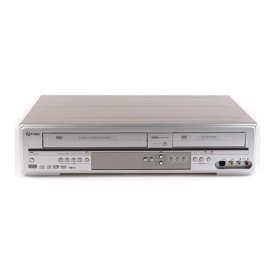
DVD/Video Cassette Recorder with HDD
HDR-A2835D/HDR-B2735D
When servicing the deck
mechanism, refer to MK14 Deck
Mechanism Section.
Deck Mechanism Part No.:
N25E1FL
PAL
Advertisement
Table of Contents

Related Manuals for FUNAI HDR-A2835D


Summary of Contents for FUNAI HDR-A2835D
- Page 1 When servicing the deck I Specifications mechanism, refer to MK14 Deck I Preparation for Servicing Mechanism Section. I Adjustment Procedures I Schematic Diagrams Deck Mechanism Part No.: I CBA’s I Exploded views N25E1FL I Parts List DVD/Video Cassette Recorder with HDD HDR-A2835D/HDR-B2735D...
- Page 2 MAIN SECTION DVD/Video Cassette Recorder with HDD HDR-A2835D/HDR-B2735D Main Section I Specifications I Preparation for Servicing I Adjustment Procedures I Schematic Diagrams I CBA’s I Exploded Views I Parts List TABLE OF CONTENTS Specifications ................1-1-1 Laser Beam Safety Precautions .
- Page 3 SPECIFICATIONS ITEM Specifications General Internal 3.5 inch HDD 160 GB Power consumption 60W (standby: 7.0W) Recording Recording format Video Recording format (DVD-RW only) Video format (DVD-RW, DVD-R) Recordable discs DVD-ReWritable DVD-Recordable Video recording format Sampling frequency 13.5MHz Compression format MPEG Audio recording format Sampling frequency 48kHz...
- Page 4 LASER BEAM SAFETY PRECAUTIONS This DVD player uses a pickup that emits a laser beam. Do not look directly at the laser beam coming from the pickup or allow it to strike against your skin. The laser beam is emitted from the location shown in the figure. When checking the laser diode, be sure to keep your eyes at least 30 cm away from the pickup lens when the diode is turned on.
- Page 5 IMPORTANT SAFETY PRECAUTIONS Product Safety Notice K. Crimp type wire connector The power transformer uses crimp type connectors Some electrical and mechanical parts have special which connect the power cord and the primary side safety-related characteristics which are often not evi- of the transformer.
- Page 6 Safety Check after Servicing Examine the area surrounding the repaired location for damage or deterioration. Observe that screws, Chassis or Secondary Conductor parts, and wires have been returned to their original positions. Afterwards, do the following tests and con- Primary Circuit firm the specified values to verify compliance with safety standards.
- Page 7 STANDARD NOTES FOR SERVICING Circuit Board Indications Pb (Lead) Free Solder When soldering, be sure to use the Pb free solder. 1. The output pin of the 3 pin Regulator ICs is indi- cated as shown. How to Remove / Install Flat Pack-IC Top View Bottom View 1.
- Page 8 3. The flat pack-IC on the CBA is affixed with glue, so With Soldering Iron: be careful not to break or damage the foil of each (1) Using desoldering braid, remove the solder from all pin or the solder lands under the IC when removing pins of the flat pack-IC.
- Page 9 2. Installation (4) Bottom of the flat pack-IC is fixed with glue to the CBA; when removing entire flat pack-IC, first apply (1) Using desoldering braid, remove the solder from soldering iron to center of the flat pack-IC and heat the foil of each pin of the flat pack-IC on the CBA up.
- Page 10 Instructions for Handling Semi-conductors Electrostatic breakdown of the semi-conductors may occur due to a potential difference caused by electro- static charge during unpacking or repair work. 1. Ground for Human Body Be sure to wear a grounding band (1MΩ) that is prop- erly grounded to remove any static electricity that may be charged on the body.
- Page 11 HANDLING PRECAUTIONS FOR HDD CAUTION: 4. OTHERS a. Be careful so as not to do the followings. 1. SHOCK Otherwise, HDD might be damaged. a. Exposing HDD to shock may be the biggest - DO NOT disassemble HDD. damaging factor. Please note that HDD is easily - When handling HDD, be sure to hold both sides damaged even if dropped from any height.
- Page 12 PREPARATION FOR SERVICING How to Enter the Service Mode About Optical Sensors Caution: An optical sensor system is used for the Tape Start and End Sensors on this equipment. Carefully read and follow the instructions below. Otherwise the unit may operate erratically. What to do for preparation Insert a tape into the Deck Mechanism Assembly and press [VCR PLAY] button.
- Page 13 CABINET DISASSEMBLY INSTRUCTIONS 1. Disassembly Flowchart REMOVAL This flowchart indicates the disassembly steps to gain REMOVE/*UNHOOK/ LOC. PART Fig. access to item(s) to be serviced. When reassembling, UNLOCK/RELEASE/ Note follow the steps in reverse order. Bend, route, and UNPLUG/DESOLDER dress the cables as they were originally. D4 4(S-7) Bracket [1] Top Cover...
- Page 14 Reference Notes 1. Locking Tabs (L-1) and (L-2) are fragile. Be careful (S-3B) not to break them. [3] Front Bracket 1-1. Remove Screw (S-2). (S-3B) 1-2. Release five Locking Tabs (L-1). (S-3) 1-3. Release three Locking Tabs (L-2) and Front Support remove the Front Assembly.
- Page 15 CN3002 [14] SW CBA CN3001 (S-7) Desolder [15] Front Jack CBA [9] ATA CBA (S-14) (S-12) [7] HDD Unit CL1001 (S-7) (S-13) HDD Rubber CN3001 [8] HDD Support [13] Power Supply CBA HDD Rubber Insulation Sheet (S-8) (S-8) Fig. D6 [6] HDD Bracket (S-16) (S-15)
- Page 16 Cylinder Assembly FE Head ACE Head Assembly SW507 LD-SW [17] Deck Assembly [18] AFV [19] Power [18] AV CBA SW CBA [17] Deck Assembly Cam Gear Hole (S-18) Shaft [18] AV CBA Desolder (S-19) Hole LD-SW [18] AV CBA Lead with blue stripe From FE Head...
- Page 17 (S-20) [20] Deck Pedestal (S-20) [21] Front Bracket R [22] Bracket R (S-22) (S-21) Fig. D9 3. How to Eject Manually Note: When rotating the gear, be careful not to damage the gear. 1. Remove the Top Cover. 2. Rotate the gear in the direction of the arrow manually as shown below. View for A Rotate this gear in the direction of the arrow...
- Page 18 ELECTRICAL ADJUSTMENT INSTRUCTIONS General Note: "CBA" is an abbreviation for "Circuit Board Assembly." NOTE: Figure 1 1.Electrical adjustments are required after replacing circuit components and certain mechanical parts. It is important to do these adjustments only after all repairs and replacements have been com- EXT.
- Page 19 HOW TO SELF-CHECK AND INITIALIZE THE DVD/VCR WITH HDD 1. Turn on the DVD/VCR with HDD recorder. 2. To put the DVD/VCR with HDD recorder into the HDD mode, press [HDD] on the remote control unit. 3. To put the DVD/VCR with HDD recorder into the self-check mode, after pressing [VARIABLE SKIP] button, press the [3], [6], and [9] buttons on the remote control in that order within three seconds.
- Page 20 Table 2: Indication of DVD self-check (*7) INDICATION DESCRIPTION Connection of DVD is normal. NOT FOUND DVD drive cannot be found. FFC cable (connecting to CN401) between the DVD drive and the DVD/HDD Main CBA is CABLE ERROR not connected correctly. Table 3: Indication of HDD self-check (*8) INDICATION DESCRIPTION...
- Page 21 FIRMWARE RENEWAL MODE 1. Update Contents 4. Load the update disc. The TV screen will display Fig. c. Item Status - If the update disc contains only a single file, the update will initiate automatically when the disc is Update B/E FIRMWARE inserted.
- Page 22 3. How to Verify the Firmware The status displayed in *2 is as shown below. Version Display Status 1. Turn the power on and remove the disc in the tray. Loading F/W from Update Disc or EXECUTING writing to Flash memory 2.
- Page 23 FUNCTION INDICATOR SYMBOLS < VCR Section > Note: If a mechanical malfunction occurs, the power is turned off. The following symbols will appear on the display. Status Display When reel or capstan mechanism is not functioning correctly When tape loading mechanism is not functioning correctly “W”...
- Page 24 < DVD/HDD Section > Note: If an error occurs, a message with the error number appears on the screen. Error message Recording Error Error No. 03-50 Message Error No. Error Description Error Example Renewal error at This code is output when there is a control information writing failure 04-50 ejecting disc due to tray being open during writing or disc loading.
- Page 25 BLOCK DIAGRAMS Servo/System Control Block Diagram E434GBLS 1-12-1...
- Page 26 Sub System Control Block Diagram E434GBLSS 1-12-2...
- Page 27 Digital Signal Process Block Diagram E434GBLD 1-12-3...
- Page 28 Video Selector Block Diagram E434GBLVS 1-12-4...
- Page 29 Video Block Diagram E434GBLV 1-12-5...
- Page 30 Audio Selector Block Diagram E434GBLAS 1-12-6...
- Page 31 Audio Block Diagram E434GBLA 1-12-7...
- Page 32 Hi-Fi Audio Selector Block Diagram E434GBLH 1-12-8...
- Page 33 Power Supply Block Diagram E434GBLP 1-12-9...
- Page 34 Sub Power Supply Block Diagram E434GBLSP 1-12-10...
- Page 35 SCHEMATIC DIAGRAMS / CBA’S AND TEST POINTS Standard Notes WARNING Many electrical and mechanical parts in this chassis have special characteristics. These characteristics often pass unnoticed and the protection afforded by them cannot necessarily be obtained by using replacement components rated for higher voltage, wattage, etc.
- Page 36 LIST OF CAUTION, NOTES, AND SYMBOLS USED IN THE SCHEMATIC DIAGRAMS ON THE FOLLOWING PAGES: 1. CAUTION: FOR CONTINUED PROTECTION AGAINST FIRE HAZARD, REPLACE ONLY WITH THE SAME TYPE FUSE. 2. CAUTION: Fixed Voltage (or Auto voltage selectable) power supply circuit is used in this unit. If Main Fuse (F1001) is blown, first check to see that all components in the power supply circuit are not defective before you connect the AC plug to the AC power supply.
- Page 37 AV 1/9 Schematic Diagram < VCR Section > 1-13-3 E434GSCAV1...
- Page 38 AV 2/9 & Sensor Schematic Diagram < VCR Section > FL601 MATRIX CHART TIME P-SCAN SHIFT TIME P-SCAN SHIFT CD R 1-13-4 E434GSCAV2...
- Page 39 AV 3/9 Schematic Diagram < VCR Section > 1-13-5 E434GSCAV3...
- Page 40 AV 4/9 Schematic Diagram < VCR Section > 1-13-6 E434GSCAV4...
- Page 41 AV 5/9 & Power SW Schematic Diagram < VCR Section > *1 NOTE These components (IC1502, C1549) can be used in any models. However, you cannot mix components under Group A with the ones under Group B. You can choose either Group. The difference between Group A and Group B is shown below.
- Page 42 AV 6/9 Schematic Diagram < VCR Section > 1-13-8 E434GSCAV6...
- Page 43 AV 7/9 Schematic Diagram < VCR Section > 1-13-9 E434GSCAV7...
- Page 44 AV 8/9 Schematic Diagram < VCR Section > E434GSCAV8 1-13-10...
- Page 45 AV 9/9 Schematic Diagram < VCR Section > E434GSCAV9 1-13-11...
- Page 46 Power Supply Schematic Diagram < VCR Section > CAUTION ! CAUTION ! NOTE: Fixed voltage (or Auto voltage selectable) power supply circuit is used in this unit. For continued protection against fire hazard, The voltage for parts in hot circuit is measured using If Main Fuse (F1001) is blown , check to see that all components in the power supply replace only with the same type fuse.
- Page 47 Front Jack & SW Schematic Diagram < VCR Section > E434GSCFJ 1-13-13...
- Page 48 Rear Jack Schematic Diagram < VCR Section > ATA Schematic Diagram < DVD/HDD Section > E434GSCRJ E434GSCAT 1-13-14...
- Page 49 AFV Schematic Diagram < VCR Section > E434GSCAFV 1-13-15...
- Page 50 DVD/HDD MAIN 1/6 Schematic Diagram < DVD/HDD Section > 1-13-16 E434GSCD1...
- Page 51 DVD/HDD MAIN 2/6 Schematic Diagram < DVD/HDD Section > 1-13-17 E434GSCD2...
- Page 52 DVD/HDD MAIN 3/6 Schematic Diagram < DVD/HDD Section > 1-13-18 E434GSCD3...
- Page 53 DVD/HDD MAIN 4/6 Schematic Diagram < DVD/HDD Section > 2 NOTE: The order of pins shown in this diagram is different from that of actual IC601. IC601 is divided into six and shown as IC601 (1/6) ~ IC601 (6/6) in this DVD/HDD Main Schematic Diagram Section. 1-13-19 E434GSCD4...
- Page 54 DVD/HDD MAIN 5/6 Schematic Diagram < DVD/HDD Section > 2 NOTE: The order of pins shown in this diagram is different from that of actual IC601. IC601 is divided into six and shown as IC601 (1/6) ~ IC601 (6/6) in this DVD/HDD Main Schematic Diagram Section. 1-13-20 E434GSCD5...
- Page 55 DVD/HDD MAIN 6/6 Schematic Diagram < DVD/HDD Section > 2 NOTE: The order of pins shown in this diagram is different from that of actual IC601. IC601 is divided into six and shown as IC601 (1/6) ~ IC601 (6/6) in this DVD/HDD Main Schematic Diagram Section. 1-13-21 E434GSCD6...
- Page 56 AV CBA Top View Sensor CBA Top View TO SENSOR CBA (END-SENSOR) TP501 TP504 TP504 VR501 TP301 J340 S-INH RF-SW RF-SW SW-P JK2-V-OUT C-PB BHF300F01012A BHF300F01012B TO SENSOR CBA (START-SENSOR) 1-13-22 BE434AF01015A...
- Page 57 AV CBA Bottom View PIN 30 OF PIN 56 OF IC1506 IC301 PIN 3 OF CN1504 PIN 5 OF CN1504 PIN 7 OF CN1504 PIN 9 OF CN1504 PIN 17 OF CN1504 WF10 PIN 30 OF CN1501 1-13-23 BE434FA01015A...
- Page 58 Power Supply CBA Top View CAUTION ! Because a hot chassis ground is present in the power CAUTION ! supply circut, an isolation transformer must be used. For continued protection against fire hazard, Fixed voltage (or Auto voltage selectable) power supply circuit is used in this unit. Also, in order to have the ability to increase the input replace only with the same type fuse.
- Page 59 Power Supply CBA Bottom View Because a hot chassis ground is present in the power CAUTION ! CAUTION ! supply circut, an isolation transformer must be used. For continued protection against fire hazard, Fixed voltage (or Auto voltage selectable) power supply circuit is used in this unit. Also, in order to have the ability to increase the input replace only with the same type fuse.
- Page 60 Front Jack CBA Top View SW CBA Top View SW CBA Bottom View Front Jack CBA Bottom View BE434AF01022B BE434AF01022C 1-13-26...
- Page 61 Rear Jack CBA Top View Rear Jack CBA Bottom View BE434AF01022D Power SW CBA Top View Power SW CBA Bottom View ATA CBA Top View ATA CBA Bottom View BE434AF01015B BE4340F01032 1-13-27...
- Page 62 AFV CBA Top View AFV CBA Bottom View 1-13-28 BE6800F01091...
- Page 63 WAVEFORMS NOTE: Input: COLOR BAR SIGNAL (WITH 1KHz AUDIO SIGNAL) Pin 9 of CN1504 Pin 17 of CN1504 Pin 56 of IC301 V-OUT E-E 0.2V 20µs VIDEO-C 0.2V 20µs AUDIO(L)-OUT 0.5ms Pin 56 of IC301 UPPER Pin 30 of IC1506 Pin 30 of CN1501 TP504 WF10...
- Page 64 WIRING DIAGRAMS Wiring 1/2 Diagram 1-15-1 E434GWI1...
- Page 65 Wiring 2/2 Diagram E434GWI2 1-15-2...
- Page 66 IC PIN FUNCTION DESCRIPTIONS < VCR Section > Signal Function Name IC501( SERVO / SYSTEM CONTROL IC ) 33 OUT D-REC-H Delayed Record Signal System Reset Signal Signal IN RESET Function (Reset=”L”) Name IN Xcin Sub Clock Not Used 36 OUT Xcout Sub Clock IN PG-DELAY Video Head Switching Pulse Signal Adjusted Voltage...
- Page 67 Notes: Signal Function Abbreviation for Active Level: Name PWM -----Pulse Wide Modulation 68 OUT DRV-DATA VFD Driver IC Control Data A/D--------Analog - Digital Converter VFD Driver IC Chip Select 69 OUT DRV-STB Signal IC612 (FRONT PANEL CONTROL) 70 OUT DRV-CLK VFD Driver IC Control Clock 71 OUT IIC-BUS- Signal...
- Page 68 LEAD IDENTIFICATIONS KRA103M-AT/P 2SA1015-GR(TE2 F T) KIA4558P/P KIA431-AT/P KRA104M-AT/P 2SA1020-Y(TE6 F M) RC4580IP KRC103M-AT/P 2SC1815-(BL,GR,Y)(TE2 F T) UTC4580 DIP-8 KTA-1266-GR-AT/P 2SC2120-(Y)(TE2 F T) KTA1267-(GR,Y)-AT/P 2SC3266-(GR,Y)(TPE2 F) KTA1281Y-AT/P KTC3203-Y-AT/P KTC3193-Y-AT/P KTC3205-Y-AT/P 1: R KTC3199-(GR,BL,Y)-AT/P KTC3198-(GR,Y)-AT/P 2: A RN1206 KTC3266-(GR,Y)-AT/P 3: K 1 2 3 E C B E C B...
- Page 69 EXPLODED VIEWS Cabinet L-12 A,B,C,D,E See Electrical Parts List for parts with this mark. B-24 D,E,F Rear Jack CBA AFV CBA B-10 JW2001 B-15 Sensor CBA Sensor CBA ATA CBA B-19 B-31 AV CBA L-15 L-15 L-11 L-15 B-22 B-21 B-16 B-22 B-32...
- Page 70 Packing [HDR-A2835D] X-3D X-2A X-2B X-26 X-3C X-3B X-3A X-3G X-3F X-3E Lower Side Upper Side X-22 S-10 1-18-2 E434GPEX...
- Page 71 Packing [HDR-B2735D] X-2B X-2A Lower Side Upper Side S-11 1-18-3 E434GPEX...
- Page 72 Comparison Chart of Models and Marks B-22A HDD RUBBER E4350JD 1VM422863 B-22B HDD RUBBER E4350JD 1VM422863 Model Mark B-22C HDD RUBBER E4350JD 1VM422863 HDR-A2835D B-22D HDD RUBBER E4350JD 1VM422863 HDR-B2735D B-32 INSULATION SHEET E434AED 1VM424477 FM1001 DC FAN MOTOR 2410RL-04W-S20-C01 MMEZR12NM005 Ref. No. Mark Description Part No.
- Page 73 Ref. No. Mark Description Part No. L-10C SCREW S-TIGHT M3X8 BIND HEAD+ GBJS3080 L-10D SCREW S-TIGHT M3X8 BIND HEAD+ GBJS3080 L-10E SCREW S-TIGHT M3X8 BIND HEAD+ GBJS3080 L-10F SCREW S-TIGHT M3X8 BIND HEAD+ GBJS3080 L-10G SCREW S-TIGHT M3X8 BIND HEAD+ GBJS3080 L-10H SCREW S-TIGHT M3X8 BIND HEAD+...
- Page 74 ALUMINUM ELECTROLYTIC CAP 10µF/ CE1CMAVSM100 16V H7 Model Mark C313 ELECTROLYTIC CAP . 1µF/50V M H7 or CE1JMAVSL1R0 HDR-A2835D ALUMINUM ELECTROLYTIC CAP 1µF/ CE1JMAVSM1R0 50V H7 HDR-B2735D C314 CHIP CERAMIC CAP .(1608) B K 0.01µF/ CHD1JK30B103 DVD MECHANISM & DVD/HDD MAIN C315 CHIP CERAMIC CAP .(1608) B K 0.047µF/...
- Page 75 Ref. No. Mark Description Part No. Ref. No. Mark Description Part No. C339 CHIP CERAMIC CAP . CH J 120pF/50V CHD1JJ3CH121 C452 ELECTROLYTIC CAP . 10µF/16V M H7 or CE1CMAVSL100 C340 ELECTROLYTIC CAP . 1µF/50V M H7 or CE1JMAVSL1R0 ALUMINUM ELECTROLYTIC CAP 10µF/ CE1CMAVSM100 16V H7 ALUMINUM ELECTROLYTIC CAP 1µF/...
- Page 76 Ref. No. Mark Description Part No. Ref. No. Mark Description Part No. C481 ELECTROLYTIC CAP . 10µF/16V M H7 or CE1CMAVSL100 C535 CHIP CERAMIC CAP .(1608) F Z 0.1µF/ CHD1JZ30F104 50V or ALUMINUM ELECTROLYTIC CAP 10µF/ CE1CMAVSM100 16V H7 CHIP CERAMIC CAP .(1608) F Z 0.1µF/ CHD1EZ30F104 C482 CHIP CERAMIC CAP .(1608) F Z 0.1µF/...
- Page 77 Ref. No. Mark Description Part No. Ref. No. Mark Description Part No. CHIP CERAMIC CAP .(1608) F Z 0.1µF/ CHD1EZ30F104 C1549 CHIP CERAMIC CAP .(1608) B K 0.1µF/ CHD1JK30B104 C1514 CHIP CERAMIC CAP .(1608) F Z 0.1µF/ CHD1JZ30F104 IC1502 SYSTEM RESET IC PST3619NR QSZBA0TMM151 50V or C1550...
- Page 78 Ref. No. Mark Description Part No. Ref. No. Mark Description Part No. C1582 CHIP CERAMIC CAP .(1608) F Z 0.1µF/ CHD1JZ30F104 C1610 ELECTROLYTIC CAP . 1µF/50V M or CE1JMASDL1R0 50V or ELECTROLYTIC CAP 1µF/50V M CE1JMASTM1R0 CHIP CERAMIC CAP .(1608) F Z 0.1µF/ CHD1EZ30F104 C1611 ELECTROLYTIC CAP .
- Page 79 Ref. No. Mark Description Part No. Ref. No. Mark Description Part No. CHIP CERAMIC CAP .(1608) F Z 0.1µF/ CHD1EZ30F104 D1509 RECTIFIER DIODE 1N4005 or NDQZ001N4005 RECTIFIER DIODE 1N4005 NDWZ001N4005 C1659 ELECTROLYTIC CAP . 47µF/6.3V M or CE0KMASDL470 D1510 RECTIFIER DIODE 1N4005 or NDQZ001N4005 ELECTROLYTIC CAP .
- Page 80 Ref. No. Mark Description Part No. Ref. No. Mark Description Part No. ZENER DIODE DZ-11BSAT265 NDTA00DZ11BS C1549 CHIP CERAMIC CAP .(1608) B K 0.1µF/ CHD1JK30B104 D1536 ZENER DIODE MTZJT-7711A or QDTA00MTZJ11 IC1503 IC SHUNT REGULATOR KIA431-AT/P NSZBA0TJY036 DIODE ZENER 11BSA-T26 or NDTA011BST26 IC1504 MICROCONTROLLER 8BIT MN101C77A...
- Page 81 Ref. No. Mark Description Part No. Ref. No. Mark Description Part No. Q516 CHIP TRANSISTOR KTC3875S-GR-RTK/ NQ14KTC3875S TRANSISTOR 2SC1815-GR(TE2 F T) QQS12SC1815F Q1536 TRANSISTOR KTA-1266-GR-AT/P or NQS4KTA1266P Q517 CHIP TRANSISTOR KTC3875S-GR-RTK/ NQ14KTC3875S TRANSISTOR 2SA1015-GR(TE2 F T) QQS12SA1015F Q1537 TRANSISTOR KTC3199-Y-AT/P or NQSYKTC3199P Q518 TRANSISTOR KTC3199-Y-AT/P or...
- Page 82 Ref. No. Mark Description Part No. Ref. No. Mark Description Part No. RES CHIP 1608 1/10W J 1.2k Ω RES CHIP 1608 1/10W J 5.6k Ω RRXA122YF002 RRXA562YF002 CHIP RES. 1/10W J 4.7k Ω or CHIP RES. 1/10W J 22k Ω or R326 RRXAJR5Z0472 R452...
- Page 83 Ref. No. Mark Description Part No. Ref. No. Mark Description Part No. CARBON RES. 1/6W J 10k Ω or RES CHIP 1608 1/10W J 1.2k Ω R545 RCX6JATZ0103 RRXA122YF002 CARBON RES. 1/4W J 10k Ω CHIP RES. 1/10W J 1.5k Ω or RCX4JATZ0103 R629 RRXAJR5Z0152...
- Page 84 Ref. No. Mark Description Part No. Ref. No. Mark Description Part No. CHIP RES. 1/10W J 820 Ω or RES CHIP 1608 1/10W J 6.8k Ω R1523 RRXAJR5Z0821 RRXA682YF002 RES CHIP 1608 1/10W J 820 Ω CHIP RES. 1/10W J 68k Ω or RRXA821YF002 R1570 RRXAJR5Z0683...
- Page 85 Ref. No. Mark Description Part No. Ref. No. Mark Description Part No. CHIP RES. 1/10W J 6.8k Ω or CHIP RES. 1/10W J 2.2k Ω or R1618 RRXAJR5Z0682 R1659 RRXAJR5Z0222 RES CHIP 1608 1/10W J 6.8k Ω RES CHIP 1608 1/10W J 2.2k Ω RRXA682YF002 RRXA222YF002 CHIP RES.
- Page 86 Ref. No. Mark Description Part No. Ref. No. Mark Description Part No. RES CHIP 1608 1/10W J 1.0M Ω RRXA105YF002 SW524 TACT SWITCH KSM0614B or SST0101HH013 CHIP RES. 1/10W J 1M Ω or R1706 RRXAJR5Z0105 TACT SWITCH SKQSAF001A or SST0101AL041 RES CHIP 1608 1/10W J 1.0M Ω...
- Page 87 POWER SW CBA Ref. No. Mark Description Part No. FILM CAP .(P) 0.039µF/50V J or CMA1JJP00393 Ref. No. Mark Description Part No. FILM CAP .(P) 0.039µF/50V J or CA1J393MS029 POWER SW CBA (AV PCB B) ---------- POLYESTER FILM CAP . (PB FREE) CA2A393DT018 Consists of the following: 0.039µF/100V J...
- Page 88 Ref. No. Mark Description Part No. Ref. No. Mark Description Part No. DIODES DIODE SWITCHING 1N4148-F0021 or NDTZ01N4148F SWITCHING DIODE 1N4148M NDTZ01N4148M D013 RECTIFIER DIODE BA158 or NDQZ000BA158 D1116 SWITCHING DIODE 1SS133(T-77) or QDTZ001SS133 RECTIFIER DIODE BA158 NDWZ000BA158 DIODE SWITCHING 1N4148-F0021 or NDTZ01N4148F D014 SCHOTTKY BARRIER DIODE SB390 or...
- Page 89 CHIP RES. 1/10W F 1k Ω or RRXAFR5Z1001 TRANSISTOR 2SA1015-GR(TE2 F T) QQS12SA1015F RES CHIP 1608 1/10W F 1.00k Ω RTW1001YF002 Q1102 TRANSISTOR S2Y52(FUNAI Q H) QQWZ00S2Y52Q CHIP RES.(1608) 1/10W 0 Ω or R1114 RRXAZR5Z0000 Q1103 TRANSISTOR KTC3199-Y-AT/P or NQSYKTC3199P RES CHIP 1608 1/10W J 0 Ω...
- Page 90 Ref. No. Mark Description Part No. Ref. No. Mark Description Part No. METAL OXIDE FILM RES. 2W J 82 Ω or R1134 RN02820ZU001 AC1001 AC CORD PE8G2X91H0AA061 WAB0182LW016 METAL OXIDE FILM RES. 2W J 82 Ω RN02820KE010 B-5A POWER HEATSINK E4340UD 1VM422057 CHIP RES.
- Page 91 SW CBA Ref. No. Mark Description Part No. RES CHIP 1608 1/10W J 220 Ω RRXA221YF002 Ref. No. Mark Description Part No. CARBON RES. 1/6W J 150 Ω R3010 RCX6JATZ0151 SW CBA (PW/SW-C) ---------- CARBON RES. 1/6W J 47 Ω or R3011 RCX6JATZ0470 Consists of the following:...
- Page 92 AFV CBA Ref. No. Mark Description Part No. DIODE ZENER 11BSA-T26 or NDTA011BST26 Ref. No. Mark Description Part No. ZENER DIODE DZ-11BSAT265 NDTA00DZ11BS AFV CBA 1VSA12639 D2004 ZENER DIODE MTZJT-7711A or QDTA00MTZJ11 Consists of the following: DIODE ZENER 11BSA-T26 or NDTA011BST26 CAPACITORS ZENER DIODE DZ-11BSAT265...
- Page 93 Ref. No. Mark Description Part No. CHIP RES.(1608) 1/10W 0 Ω or RRXAZR5Z0000 RES CHIP 1608 1/10W J 0 Ω RRXA000YF002 CHIP RES.(1608) 1/10W 0 Ω RRXAZR5Z0000 RES CHIP 1608 1/10W J 0 Ω RRXA000YF002 MISCELLANEOUS XTAL 18.432MHz FXD186LLN001 ATA CBA Ref.
- Page 94 HDR-A2835D/HDR-B2735D E434GED/JBD 2007-01-10...