Table of Contents
Advertisement
Colour Television
Contents
Waveforms
SSB: Sound Processor
©
Copyright 2006 Philips Consumer Electronics B.V. Eindhoven, The Netherlands.
All rights reserved. No part of this publication may be reproduced, stored in a
retrieval system or transmitted, in any form or by any means, electronic,
mechanical, photocopying, or otherwise without the prior permission of Philips.
Published by WS 0664 BG CD Customer Service
Page
Contents
2
5
8
9
19
20
21
22
23
24
25
Diagram PWB
(A1) 26
33-38
(A2) 27
33-38
(A3) 28
33-38
(A4) 29
33-38
(A5) 30
33-38
(A6) 31
33-38
(A7) 32
33-38
(B1) 39
51-52
(B2) 40
51-52
(B3) 41
51-52
(B4) 42
51-52
(B5) 43
51-52
(B6) 44
51-52
(B7) 45
51-52
(B8) 46
51-52
(B9) 47
51-52
(B10) 48
51-52
(B11) 49
51-52
Printed in the Netherlands
Subject to modification
Chassis
L06.1E
AA
G_15950_000.eps
050406
Page
(B12) 50
51-52
54
(F) 55
56
58
59
64
65
69
70
77
EN 3122 785 16350
Advertisement
Table of Contents

Related Manuals for Philips L06.1E AA


Summary of Contents for Philips L06.1E AA
-
Page 1: Table Of Contents
All rights reserved. No part of this publication may be reproduced, stored in a retrieval system or transmitted, in any form or by any means, electronic, mechanical, photocopying, or otherwise without the prior permission of Philips. Published by WS 0664 BG CD Customer Service... -
Page 2: Technical Specifications, Connections, And Chassis Overview
EN 2 L06.1E 1. Technical Specifications, Connections, and Chassis Overview Index of this chapter: 1.1 Technical Specifications 1.2 Connection Overview 1.3 Chassis Overview Note: Data below can deviate slightly from the actual situation, due to the different set executions. Technical Specifications 1.1.1 Vision Display type... - Page 3 Technical Specifications, Connections, and Chassis Overview EXT1: Video RGB - In, CVBS - In/Out, Audio - In/Out E_06532_001.eps 050404 Figure 1-3 SCART connector - Audio R 0.5 V / 1 kohm - Audio R 0.5 V / 10 kohm - Audio L 0.5 V / 1 kohm - Ground Audio...
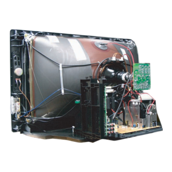
- Page 4 EN 4 L06.1E Chassis Overview CONTROL PANEL SIDE I/O PANEL SMALL SIGNAL BOARD Technical Specifications, Connections, and Chassis Overview Figure 1-6 PWB location CRT PANEL FRONT INTERFACE PANEL LARGE SIGNAL PANEL G_16350_043.eps 060406...
-
Page 5: Safety Instructions, Warnings, And Notes
2. Safety Instructions, Warnings, and Notes Index of this chapter: 2.1 Safety Instructions 2.2 Maintenance Instructions 2.3 Warnings 2.4 Notes Safety Instructions Safety regulations require the following during a repair: • Connect the set to the Mains/AC Power via an isolation transformer (>... - Page 6 Safety Instructions, Warnings, and Notes 2.4.4 Lead-free Solder Philips CE is producing lead-free sets (PBF) from 1.1.2005 onwards. Identification: The bottom line of a type plate gives a 14-digit serial number. Digits 5 and 6 refer to the production year, digits 7 and 8 refer to production week (in example below it is 1991 week 18).
- Page 7 2.4.5 Alternative BOM identification In September 2003, Philips CE introduced a change in the way the serial number (or production number, see Figure 2-2) is composed. From this date on, the third digit in the serial number (example: AG2B0335000001) indicates the number of the alternative BOM (Bill of Materials used for producing the specific model of TV set).
-
Page 8: Directions For Use
EN 8 L06.1E Directions for Use 3. Directions for Use You can download this information from the following websites: http://www.philips.com/support http://www.p4c.philips.com... -
Page 9: Mechanical Instructions
4. Mechanical Instructions Index of this chapter: 4.1 Service Connector (for IAP) 4.2 Set Disassembly 4.3 Service Positions 4.4 Assy / Board Removal 4.5 Set Re-assembly Note: Figures below can deviate slightly from the actual situation, due to the different set executions. Service Connector (for IAP) For software uploading with the IAP tool (In Application Programming), it is not necessary to remove EEPROMs from... - Page 10 EN 10 L06.1E Assy / Board Removal Sometimes, it can be necessary to swap a complete assy or Printed Wiring Board (PWB). How that can be done is explained below. 4.4.1 Top Control & Side I/O Assy/Panel Figure 4-3 Top control & Side I/O assy/panel 1.
- Page 11 4.4.4 Large Signal Panel (LSP) Figure 4-7 LSP locking handles 1. Simultanuously do the following: a. Pull the two plastic locking handles at the mid left and mid right side of the bracket gently backwards to unlock the bracket (see Figure “LSP locking handles”), b.
-
Page 12: Service Modes, Error Codes, And Fault Finding
EN 12 L06.1E 5. Service Modes, Error Codes, and Fault Finding Index of this chapter: 5.1 Test Points 5.2 Service Modes 5.3 Problems and Solving Tips Related to CSM 5.4 Service Tools 5.5 Error Codes 5.6 The Blinking LED Procedure 5.7 Software Downloading 5.8 Fault Finding and Repair Tips Test Points... - Page 13 Service Modes, Error Codes, and Fault Finding How to Navigate When you press the MENU button on the remote control, the set will switch on the normal user menu in the SDM mode. How to Exit Switch the set to STANDBY by pressing the POWER button on the remote control transmitter.
- Page 14 EN 14 L06.1E 1 00025 L06EF1 1.2 2 CODES 0 0 0 0 0 3 OP 136 008 006 000 000 002 016 5 CTN 7 PAL 8 DUAL I 9 C O 5 0 C L 5 0 B R 5 0 H U 0 AVL Off Figure 5-4 CSM menu (example) Menu Explanation...
- Page 15 Service Modes, Error Codes, and Fault Finding Figure 5-5 IAP interface 16V10u 1N4148 SDA2 SN74LS05 SDA1 SDA2 SCL2 1N4148 1N4148 SCL1 SCL2 SDA1 SN74LS05 1N4148 SCL1 Figure 5-6 IAP interface circuit diagram Installing the IAP software on a PC When all the items mentioned above are present, install the software on a PC as follows: •...
- Page 16 EN 16 L06.1E Table 5-2 Error Table Error Description 0 = No error High beam (BCI) protection Vertical guard protection POR bit / +8 V protection Black current loop instability protection General I C error Microprocessor (M30620FCNGP) C error while communicating with the PLL tuner (UV1316E) C error while communicating with the EEPROM (NVM at uP, M24C64)
- Page 17 Service Modes, Error Codes, and Fault Finding Table 5-3 NVM default values Default values (hex) Item EW (EW Width) PW (EW Parabola Width) HS (Horizontal Shift) HP (Horizontal Parallelogram) HB (Horizontal Bow) UCP (EW Upper Corner Parabola) LCP (EW Lower Corner Parabola) TC (EW Trapezium) VS (Vertical Slope) VA (Vertical Amplitude)
- Page 18 5.8.2 SAM Menu Structure The SAM Menu structure of the L06.1E AA is different from that of the ES1. Some of the menu items that were in the main menu of the ES1 are now in the submenu. The following table shows the structure of the SAM menu of the L06.1E AA.
-
Page 19: Block Diagrams, Testpoint Overviews, And
HEADPH. TOP CONTROL (SL06) CVBS LEFT RIGHT SVHS 8252 1580 1587 1581 1586 SMALL SIGNAL BOARD 1400 1582 8400 L06.1E AA AQUADAG 1317 CRT PANEL 1340 1336 8361 SOCKET BLACK 1335 1382 1361 1351 1504 LSP(LARGE SIGNAL PANEL) 8254 1542... -
Page 20: Block Diagram Lsp Supply And Deflection
3513 DRAIN 3514 DRIVER 3522 SENCE 3517 CTRL DEMAG 7510 TEA1507 DRAIN DRIVER SENCE CTRL 3580 DEMAG 7532 3597 L06.1E AA 7541 ENERGIZING +Vaudio 1503 CIRCUIT 5512 6551 5551 6500 5552 Vbatt 6563 5562 5566 -Vaudio 7512 5511 5561 6562... -
Page 21: Testpoint Overview Lsp
F453 C7 F464 F6 F478 D9 F503 G1 F537 C5 F573 D6 F582 C3 F631 B8 F677 B9 3139 123 5895.4 L06.1E AA F678 C6 F706 C10 F715 B9 F722 B10 F910 B3 F955 B4 I241 A6 I255 A7 I413 D6... -
Page 22: Block Diagram Video
SII9011CLU RX2+ RX2- HDMI RX1+ RX1- RX0+ RX0- HSYNC RXC+ VSYNC RXC- DSCL ODCK DSDA HDMI 7308 CONNECTOR HDMI_EN L06.1E AA 7061 TDA9886T/V4 1002 VIF1 VIF1 VIF2 VIF2 1003 DEMODULATOR SIF1 SIF1 SIF2 SIF2 SC1_CVBS_OUT CVBS 7150 SVPEX42 7721 SVPEX42... -
Page 23: Block Diagram Audio
7307 7961 SII9011CLU UDA1334BT/N2 AUDIO HDMI I2SSCK HDMI_R I2SWS MA(0-11) HDMI_L I2SDI1 DATAI HD_AUDIO_SEL2 SYSCLK MCLK SYSCLK HDMI CONNECTOR L06.1E AA 7061 TDA9886T/V4 1002 VIF1 VIF1 VIF2 VIF2 1003 DEMODULATOR SIF1 SIF1 SIF2 SIF2 AGC-IF SIOMAD SOUND PROCESSOR 7907 MSP3411G-QI-B8V3... -
Page 24: I2C Overview
MICROPROCESSOR +3V3STBY 7201 M30620SPGP 3241 3243 RENEAS MICRO PROCESSOR 3228 SDA_EE 3227 SCL_EE +3V3STBY 7203 M24C64 EEPROM E_PAGE L06.1E AA TUNER IF & DEMODULATOR SVPEX42 1000 7061 7721 SVPEX42 UV1316E TDA9886T TUNER TRIDENT VIDEO DEMODULATOR ADDRESS PROCESSOR DATA HDMI +3V3_HDMI... -
Page 25: Supply Lines Overview
3536 DRIVER SENCE CTRL 3580 DEMAG 7532 3597 DEFLECTION Vbatt 5402 7404 HDRIVE 6465 LINE OUTPUT EW_DRIVE CIRCUIT CORRECTION L06.1E AA 7541 ENERGIZING +Vaudio +Vaudio 1503 CIRCUIT -Vaudio 5512 6551 5551 5552 Vbatt 5562 6563 5566 -Vaudio +Vaudio A3,A4 -Vaudio... -
Page 26: Circuit Diagrams And Pwb Layouts
BURST ON-TIME POWER DETECTOR PROTECTION PROTECTION 3597 220K 3524 3595 3521 2521 7549-1 100K IMX1 7549-2 IMX1 3139 123 5895.6 L06.1E AA +Vaudio 1503 LKS1AF 7541 BC857B 5502 6551 SP48012-00 BYT28 5551 9506 2506 3508 6500 GBU4J Audio_Gnd 220R 2551 "$"... -
Page 27: Lsp: Deflection (A2)
2425 BAS316 3437 22K 2437 2426 2422 100n GND_EW GND_EW GND_HOR GND_EW GND_EW MainSupplyGnd 3139 123 5895.6 GND-LINEDRIVE GND_EW GND_HOR L06.1E AA 9410 5410 2427 3433 GND_HOR 5450 JF0101 5401 L.LIN 2431 TO PICTURE TUBE 680p 1404 FOCUS B2P-VA-BF SCREEN... -
Page 28: Lsp: Class D Audio Amplifier (Res) (A3)
100n 7901-2 LM393N AUDIO-SW 3938 1904 2938 3941 3939 VOL_MUTE AUDIO-R 100R Audio_Gnd Audio_Gnd AUDIO-L AUDIO-C B6B-PH-K 3139 123 5895.6 L06.1E AA 6906 Vaudio+ BAV99 2951 Vaudio- 2977 2961 2950 Audio_Gnd Audio_Gnd 2949 3960 470u 100K 2948 Audio_Gnd 2947 6905... -
Page 29: Lsp: Audio Amplifier (A4)
AUDIO-R F951 3991 Audio_Gnd Audio_Gnd VOL_MUTE SUB_MUTE 7962 BC857B For Europe Audio_Gnd ITEM 1910 1911 4984 7962 9916 3139 123 5895.6 L06.1E AA Audio_Gnd 7990 +15V9 TDA2616Q OUT1 2989 INV1- 220n +15V9 MUTE V|GND Audio_Gnd INV2- Audio_Gnd OUT2 2992 INV12... -
Page 30: Lsp: Tuner If (Res) (A5)
9230 TO 1587 OF +5.2V 9231 9233 +33V AUDIO-SL 9234 B8B-EH-A B3B-EH-A 9235 3139 123 5895.6 L06.1E AA 2251 B4 3238 C2 3240 B4 3242 B5 5247 B10 5249 B3 5251 B5 2268 C7 3239 B4 3241 B4 4220 D1... -
Page 31: Lsp: Interfacing (A6)
B4B-EH-A B5B-EH-A 1608 1670 SIMM For Europe ITEM 1620 1623 1624 1625 1645 4683 4694 9620 9621 9626 3139 123 5895.6 L06.1E AA 1621 7675 SI2305DS B5B-EH-A 7676 BC847BW Vaux_GND 7674 KA78R08 Φ +9VA 5682 2692 VDIS 2674 2691 Vaux_GND... -
Page 32: Lsp: Scart I/O (Res) (A7)
5708 For Europe 29RF A68ERF182X044 ITEM 3725 USED 9702 USED 9703 USED USED 9704 9705 USED 9706 USED 3139 123 5895.6 L06.1E AA 3703 3704 R-SC2-OUT R-SC1_AV1-IN 150R 150R 3709 3710 L-SC2-OUT 150R 150R 3711 L-SC1_AV1-IN 100R SC1-STATUS 3714 3717... -
Page 33: Layout Lsp (Top Side)
1502 A2 1543 C4 1621 G8 1645 E5 1901 E3 2402 A8 2413 C7 2450 A9 2469 C9 3139 123 5895.6 L06.1E AA 2488 A7 2505 A4 2524 E4 2542 B4 2570 C4 2692 E7 2984 F3 3413 A7 3426 C7... - Page 34 2493 A1 2499 E1 2517 A4 2538 D7 2572 D5 Part 1 G_16350_009a.eps Part 3 G_16350_009c.eps 3139 123 5895.6 L06.1E AA 2575 D5 2586 C6 2666 G5 2673 G4 2681 F3 2695 F4 2705 D1 2713 F1 2719 D1 2914 G7...
- Page 35 Circuit Diagrams and PWB Layouts L06.1E AA Layout LSP (Part 1 Bottom Side) Part 1 G_16350_009a.eps 230306...
- Page 36 Circuit Diagrams and PWB Layouts L06.1E AA Layout LSP (Part 2 Bottom Side) Part 2 G_16350_009b.eps 230306...
- Page 37 Circuit Diagrams and PWB Layouts L06.1E AA Layout LSP (Part 3 Bottom Side) Part 3 G_16350_009c.eps 230306...
- Page 38 Circuit Diagrams and PWB Layouts L06.1E AA Layout LSP (Part 4 Bottom Side) Part 4 G_16350_009d.eps 230306...
-
Page 39: Ssb: Power Supply & Connectivities (B1)
AUDIOSW 4563 1584 POWER_DOWN B1,B2,B7 +9VA TO 1904 OF +5V2 CONNECTIVITIES " 560 ~ 569 " " 580 ~ 599 " 3139 123 6086.3 L06.1E AA FRONT INTERFACE PANEL 1586 7500 LF80CPT +9VA 1581 3501 7504 PDTC114ET SIDE AV STBY_CON... -
Page 40: Ssb: Micro Processor (B2)
HLDA 3247 7204-1 HOLD 3248 74HC02D ALE_EMU 100R 3249 CLKOUT P5<0:7> 7204-2 7204-4 7204-3 74HC02D 74HC02D 74HC02D 3139 123 6086.3 L06.1E AA +3V3STBY Φ AVCC 3209 100R 3208 100R KEYBOARD 3207 100R LIGHT_SENSOR 3206 100R SC1_STATUS 3205 100R SC2_STATUS 75i_Con... -
Page 41: Ssb: Tuner If & Demodulator (B3)
SIF1 SIF1 OUTPUT SUPPLY I C-BUS TRANSCEIVER PORTS +5VS 2071 3066 +5VS 3067 B2,B4,B6,B7,B8 2073 3068 B2,B4,B6,B7,B8 2074 3139 123 6086.3 L06.1E AA 6000 BAS316 6001 3001 4000 5000 120R 1002 38M9 3008 IGND 4004 4005 1003 4006 ISWI 4007... -
Page 42: Ssb: Svpex42 (B4)
2752 2750 100n 2753 2751 2747 100n VDDMQ 100n VDDC VDDH VDDM SUPPLY_DIG VSSC VSSH VSSM VD1_8 3139 123 6086.3 L06.1E AA 5721 VL1_8 220R +3V3 5722 VA1_8 VA1_8 5723 220R 2781 220R 2782 100n 5724 220R AVDD_ADC PAVDD SUPPLY_ANA... -
Page 43: Ssb: Ddr Dram & Supply (B5)
3717 DQM1 DQM3 DQM0 DQM2 MA10 MA11 DDR VDDMQ / VDDM de-caps VDDMQ SDRAM Decoupling Capacitors VDDMQ VDDMQ 3139 123 6086.3 L06.1E AA VDDMQ 7701 Φ VREF VDDQ SDRAM 1M X 32 X 4 3707-1 MD15 3707-2 MD14 3707-3 MD13... -
Page 44: Ssb: Hdmi (B6)
DC1R019JDA +5VHDMI +3V3_HDMI +5VHDMI 7304 BSN20 DSCL (256x8) +3V3 EEPROM 7305 DSDA BSN20 1302 146280-2 3139 123 6086.3 FOR TEST JIG L06.1E AA 5302 +3V3 5303 +1V8_HDMI 5304 +3V3 220R +3V3_HDMI 7307 2347 SII9011CLU No Comp 1301 3307 25M322 3336... -
Page 45: Ssb: Deflection Controller (B7)
FBLINK VSYNC 3426 HSYNC 3427 CUT_OFF 3429 3434 3435 3437 EHT_INFO 3442 470K 6405 3445 330K BAS316 3139 123 6086.3 L06.1E AA 2400 2401 100n 100R 3402 3404 100R 100R 3406 7401 TDA9330H/N3 Φ TV DISPLAY 3413 2410 PROCESSORS LPSU... - Page 46 2913 SC4-IN-R SC4-IN-L SCART 4 HD_DVI_R 2954 HD_DVI_L 2955 2914 2915 I2SSCK 4935 I2SWS 4936 AUDIOSW 3139 123 6086.3 L06.1E AA interface interface RESETQ I2SL/R I2SL/R S1...4 DACM-R LOUDSPEAKER R NICAM A LOUDSPEAKER NICAM B DACM-L LOUDSPEAKER L IDENT IDENT...
-
Page 47: Ssb: Scart Analogue I/O (B9)
RGB-G_in S175 3178 RGB-R_in RGB-BL_in F170 3184 F159 Terr_CVBS_out F160 Video_in 3187 PPTV/90 7150 BC847B I159 3188 3139 123 6086.3 L06.1E AA F161 I153 4154 SC1_R_OUT F162 SCART 2 I154 1150-2 2155 SC1_R_IN ROW_B Audio-R_out F163 Audio-R_in I155 4156 SC1_L_OUT... -
Page 48: Ssb: Y, Pb, Pr, Ext. Input
HD-L DVI_L +3V3 6102 VEE VSS BAV99 4101 4102 7107 4103 SC1_FBL 3114 PMBT2369 B2,B9 100R HDMI_DE 3139 123 6086.3 L06.1E AA 3124 2117 DVI_L I/O SELECTION 150R 3126 2120 DVI_R 74LVC1G3157GW 150R SC1_CVBS_OUT 3108 Y_IN 100R 3101 2103 HD-L... -
Page 49: Ssb: Adc
5605 5606 2630 2631 4606 3625 100R 5607 5608 2633 2632 1601 1600 3139 123 6086.3 For Compair Only L06.1E AA +3V3ADC +3V3ADC 7601 AD9985AKSTZ-110 Φ ANALOG INTERFACE FOR 2618 RAIN FLAT PANEL DISPLAY 2619 GAIN 2620 BAIN 4607 3601... -
Page 50: Ssb: Hdmi Sound Switching
I2SSCK B6,B8 I2SWS B6,B8 I2SDI1 B6,B8 SYSCLK 4972 2972 3963 HDMI_L 100R 4973 2973 3965 HDMI_R 100R 3139 123 6086.3 L06.1E AA DAC_+3V3 DAC_+3V3 7961 UDA1334BT/N2 VDDA VDDD DIGITAL INTERFACE DATAI SFOR0 DE-EMPHASIS SFOR1 SYSCLK INTERPOLATION MUTE FILTER DEEM NOISE SHAPER... - Page 51 1601 D2 2107 D3 2207 C4 2301 D6 2348 D6 2425 B6 2510 A6 2619 D4 2636 D4 3139 123 6086.3 L06.1E AA 2922 B2 2945 B2 2963 A2 3061 C2 3140 C3 3216 C3 2637 D4 2726 C5 2754 B6...
- Page 52 2122 D1 2161 D4 2177 D4 2310 D2 2325 D2 2403 C1 2432 B1 2584 B6 2611 D2 3139 123 6086.3 L06.1E AA 2612 D3 2659 B2 2707 A3 2737 B1 2757 B2 2777 C2 2796 A2 2941 B5 3063 C5...
-
Page 53: Side I/O Panel (Sl6
Video_Gnd 1250-1 1277-1 VIDEO IN Video_Gnd Video_Gnd YELLOW Video_Gnd 3153 1250-3 RIGHT 1277-2 3151 1250-2 LEFT WHITE 3139 123 6109.1 L06.1E AA 4186 3159 100R 1254 4185 3160 1252 100R Video_Gnd 2175 4184 2u2 50V 4182 1010 2180 2u2 50V... - Page 54 Circuit Diagrams and PWB Layouts Layout Side I/O Panel (SL6) (Top Side) 3139 123 6109.1 Layout Side I/O Panel (SL6) (Bottom Side) 3139 123 6109.1 L06.1E AA 1010 B1 1011 B1 1012 B2 1013 B2 1014 B3 1232 A1 1250 A2...
-
Page 55: Crt Panel (F)
USED USED USED USED 9324 NOT USED NOT USED NOT USED NOT USED Rotation crt USED NOT USED USED NOT USED 3139 123 5817.6 L06.1E AA +141V +200A 1330 GND_RGB 3337 GND_RGB 100K GND_RGB 7330 TDA6111Q 117V MIRROR MIRROR 9301... - Page 56 Circuit Diagrams and PWB Layouts Layout CRT Panel (Top Side) 3139 123 5817.6 L06.1E AA Layout CRT (Bottom Side) 1316 B4 1317 E2 1330 D3 1331 D4 1334 D4 1335 B1 1336 D1 1340 E2 1351 A1 1354 C1 1355 C1...
-
Page 57: Front Interface Panel (Sl6
1693 3139 123 5982.1 FROM 1624 6691 INTERFACING LTL-10224WHCR L01 USA ONLY 7691 4601 3697 3139 123 5722.1 L06.1E AA Personal Notes: 1211 A1 1231 A3 1505 A4 1606 D3 1693 C1 2691 C4 2692 D2 2698 C4 3500 A2... - Page 58 Circuit Diagrams and PWB Layouts Layout Front Interface Panel (SL6) (Top Side) 3139 123 5722.1 L06.1E AA Layout Front Interface Panel (SL6) (Bottom Side) 1211 D1 1231 C3 1505 A1 1606 D4 1693 A3 2691 A4 2698 A3 3500 B2...
-
Page 59: Alignments
8. Alignments Index of this chapter: 8.1 General Alignment Conditions 8.2 Hardware Alignments 8.3 Software Alignments 8.4 Option Settings General Alignment Conditions 8.1.1 Default Alignment Settings Perform all electrical adjustments under the following conditions: • Power supply voltage: 230 V •... - Page 60 EN 60 L06.1E 8.2.2 Focus alignment The LOT has the following outline: – Focus 1 (F1) = Static alignment (red wire). – Focus 2 (F2) = Dynamic alignment (white wire). 1. Use an external video pattern generator to input a "circle" or "crosshatch"...
- Page 61 2. EWW (East-West Width): This sets the (overall) horizontal size of the picture on the screen. Range from 0 to +63. 3. EWP (East-West Parabola): Align for the vertical lines of the test picture to be straight lines. Range from 0 to +63. 4.
- Page 62 EN 62 L06.1E 8.4.3 Option Settings In the table below, you will find the option settings. Option byte & bit table for restoring the TV set to its original Factory Default Options via the NVM Editor in the SAM menu Description of feature/option to be switched ON or OFF bit 7 (msb) OP_PHILIPS_TUNER...
- Page 63 Option Bit Definition OP_PHILIPS_TUNER: Philips Tuner. Function: Choose the tuner type that is configured in the hardware. Values: OFF= Disabled, Other (non-Philips) tuner is used. ON= Enabled, Philips compatible tuner is used. OP_ACI: Automatic Channel Installation. Function: Disable/Enable automatic channel installation.
-
Page 64: Circuit Descriptions, Abbreviation List, And Ic Data Sheets
EN 64 L06.1E 9. Circuit Descriptions, Abbreviation List, and IC Data Sheets Index of this chapter: 9.1 Introduction 9.2 Small Signal Board 9.3 Software Upgrading 9.4 Abbreviation List 9.5 IC Data Sheets Note: Only new circuits (circuits that have not been published recently) are mentioned. -
Page 65: Abbreviation List
Circuit Descriptions, Abbreviation List, and IC Data Sheets Software Upgrading In this chassis, you can upgrade the software via the IAP tool (In Application Programming). This offers the possibility, to replace the entire SW image without having to remove the flash-RAM from its socket. - Page 66 EN 66 L06.1E Monochrome TV system. Sound carrier distance is 6.5 MHz. D= VHF- band, K= UHF-band Digital to Analogue Converter Dynamic Astigmatism and Focusing; a method to keep the electron spot round and focused during the whole scan Dynamic Bass Enhancement; extra low frequency amplification Direct Current Dynamic Contrast Control...
- Page 67 Circuit Descriptions, Abbreviation List, and IC Data Sheets IF-TER IF signal from main tuner Inter IC bus (also called I2C) Interlaced Scan mode where two fields are used to form one frame. Each field contains half the number of the total amount of lines.
- Page 68 EN 68 L06.1E Random Access Memory Remote Control transmitter RC5 (6) Remote Control system 5 (6), the signal from the remote control receiver Radio Data System (European); This is an MPX signal carried in FM radio channels (87.5 … 108 MHz) RESET RESET signal Real Flat (picture tube) or Radio...
-
Page 69: Ic Data Sheets
Circuit Descriptions, Abbreviation List, and IC Data Sheets VESA Video Electronics Standards Association Video Graphics Array VGND Video ground VGUARD Vertical guard voltage Video Intermediate Frequency Variable Level out; Processed audio output towards external amplifier VOL (+/-) Volume (+/-) V-SYNC-VGA V_sync on VGA connector Watch Dog Write Enable control line... -
Page 70: Spare Parts List
EN 70 L06.1E 10. Spare Parts List Sets Listed 8670 000 23687 29PT9521/12 8670 000 23759 32PW9551/12 Set Level Various 1099 9301 982 90314 W76ERF185X044 32” 1099 9301 991 30314 A68ERF185X044 29” 1116 3139 267 20471 Side I/O + Control [D] 1160 3139 267 21621 Front Interf. - Page 71 3361 4822 050 24701 470Ω 1% 0.6W 3362 2120 108 94133 R Fuse 10Ω 3363 4822 051 30561 560Ω 5% 0.062W 3364 4822 051 20108 1Ω 5% 0.1W 3365 4822 051 30472 4.7Ω 5% 0.062W 3366 4822 051 30683 68kΩ 5% 0.062W 3367 4822 116 52297 68kΩ...
- Page 72 EN 72 L06.1E 7365 4822 130 60887 BF840 7366 9352 628 51112 TDA8941p/N1 7403 4822 130 44568 BC557B 7404 9340 547 13215 BSH103 7405 9340 591 84127 ON5277 7406 9322 191 77687 STP6NK60ZFP 7406 9322 194 27687 STP3NK60ZFP 7407 4822 130 10255 MUN2213 7455 9352 637 54112 TDA4863J/V1 7510...
- Page 73 2661 5322 126 11583 10nF 10% 50V 0603 2662 5322 126 11583 10nF 10% 50V 0603 2663 5322 126 11583 10nF 10% 50V 0603 2664 5322 126 11583 10nF 10% 50V 0603 2665 5322 126 11583 10nF 10% 50V 0603 2666 5322 126 11583 10nF 10% 50V 0603 2680...
- Page 74 EN 74 L06.1E 3221 4822 051 30103 10kΩ 5% 0.062W 3222 4822 051 30103 10kΩ 5% 0.062W 3223 4822 051 30101 100Ω 5% 0.062W 3224 4822 051 30101 100Ω 5% 0.062W 3225 4822 051 30472 4.7Ω 5% 0.062W 3227 4822 051 30101 100Ω 5% 0.062W 3228 4822 051 30101 100Ω...
- Page 75 5307 4822 157 11716 Bead 30Ω at 100MHz 5308 4822 157 11716 Bead 30Ω at 100MHz 5501 2422 535 94995 10µH 20% 5502 2422 536 00339 33µH 20% 5503 2422 535 94995 10µH 20% 5504 2422 549 43062 Bead 600Ω at 100MHz 5560 2422 549 43062 Bead 600Ω...
- Page 76 EN 76 L06.1E 3366 4822 051 30683 68kΩ 5% 0.062W 3367 4822 116 52297 68kΩ 5% 0.5W 3368 4822 051 30561 560Ω 5% 0.062W 3370 4822 051 20108 1Ω 5% 0.1W 3371 2312 915 11002 1kΩ 1% 0.5W 3372 2312 915 11002 1kΩ 1% 0.5W 3373 2322 257 41152 1.5kΩ...
-
Page 77: Revision List
Revision List L06.1E EN 77 11. Revision List Manual xxxx xxx xxxx.0 • First release. - Page 78 EN 78 L06.1E Revision List...