Table of Contents
Advertisement
Note:
When the DIGITAL P.C.B. or IC82 on DIGITAL (1) P.C.B. is replaced, this unit will display "Internal Error" and will
not operate properly. The model name MUST be written to the backup IC (EEPROM: IC82 on DIGITAL (1) P.C.B.) to
have proper operation. (For detailed procedure, refer to related Service News or Service Bulletin. Or contact your
local Yamaha representative.)
This manual has been provided for the use of authorized Yamaha Retailers and their service personnel.
It has been assumed that basic service procedures inherent to the industry, and more specifi cally Yamaha Products, are already known
and understood by the users, and have therefore not been restated.
WARNING:
IMPORTANT:
The data provided is believed to be accurate and applicable to the unit(s) indicated on the cover. The research, engineering, and service
departments of Yamaha are continually striving to improve Yamaha products. Modifi cations are, therefore, inevitable and specifi cations
are subject to change without notice or obligation to retrofi t. Should any discrepancy appear to exist, please contact the distributor's
Service Division.
WARNING:
IMPORTANT:
■ CONTENTS
TO SERVICE PERSONNEL ............................................2
FRONT PANELS .........................................................3-4
REAR PANELS ...........................................................5-8
REMOTE CONTROL PANEL ..........................................9
SPECIFICATIONS ................................................... 10-14
INTERNAL VIEW .................................................... 15-16
SERVICE PRECAUTIONS ............................................ 16
DISASSEMBLY PROCEDURES ............................. 17-24
UPDATING FIRMWARE ..........................................25-27
SELF-DIAGNOSTIC FUNCTION ............................28-70
POWER AMPLIFIER ADJUSTMENT ............................71
1 0 1 2 6 7
RX-V675/HTR-6066/
RX-A730/TSR-6750
Failure to follow appropriate service and safety procedures when servicing this product may result in personal injury,
destruction of expensive components, and failure of the product to perform as specifi ed. For these reasons, we advise
all Yamaha product owners that any service required should be performed by an authorized Yamaha Retailer or the
appointed service representative.
The presentation or sale of this manual to any individual or fi rm does not constitute authorization, certifi cation or
recognition of any applicable technical capabilities, or establish a principle-agent relationship of any form.
Static discharges can destroy expensive components. Discharge any static electricity your body may have
accumulated by grounding yourself to the ground buss in the unit (heavy gauge black wires connect to this buss).
Turn the unit OFF during disassembly and part replacement. Recheck all work before you apply power to the unit.
Copyright (c) Yamaha Corporation All rights reserved.
This manual is copyrighted by Yamaha and may not be copied or
redistributed either in print or electronically without permission.
AV RECEIVER
SERVICE MANUAL
IMPORTANT NOTICE
DISPLAY DATA .......................................................72-73
IC DATA ................................................................... 74-94
PIN CONNECTION DIAGRAMS .............................95-97
BLOCK DIAGRAMS .............................................. 98-101
WIRING DIAGRAMS ........................................... 102-103
PRINTED CIRCUIT BOARDS ............................. 104-125
SCHEMATIC DIAGRAMS ................................... 127-142
REPLACEMENT PARTS LIST ............................ 143-163
REMOTE CONTROL ........................................... 164-166
ADVANCED SETUP ............................................ 167-168
FIRMWARE UPDATING PROCEDURE .............. 169-180
P.O.Box 1, Hamamatsu, Japan
'13.05
Advertisement
Table of Contents

Related Manuals for Yamaha RX-V675


Summary of Contents for Yamaha RX-V675
-
Page 1: Table Of Contents
This manual has been provided for the use of authorized Yamaha Retailers and their service personnel. It has been assumed that basic service procedures inherent to the industry, and more specifi cally Yamaha Products, are already known and understood by the users, and have therefore not been restated. -
Page 2: To Service Personnel
RX-V675/HTR-6066/RX-A730/TSR-6750 ■ TO SERVICE PERSONNEL AC LEAKAGE 1. Critical Components Information WALL EQUIPMENT TESTER OR OUTLET UNDER TEST EQUIVALENT Components having special characteristics are marked must be replaced with parts having specifications equal to those originally installed. 2. Leakage Current Measurement (For 120V Models Only) -
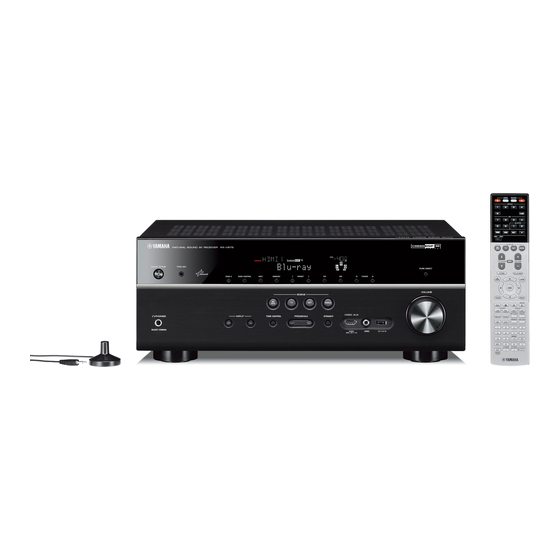
Page 3: Front Panels
RX-V675/HTR-6066/RX-A730/TSR-6750 ■ FRONT PANELS RX-V675 (U, C, R, T, A, B, G, F, L, S, H models) HTR-6066 (G, F models) - Page 4 RX-V675/HTR-6066/RX-A730/TSR-6750 RX-A730 (U, C, A, B, G, L models) TSR-6750 (U model)
-
Page 5: Rear Panels
RX-V675/HTR-6066/RX-A730/TSR-6750 ■ REAR PANELS RX-V675 (U, C models) RX-V675 (R, S models) RX-V675 (T model) - Page 6 RX-V675/HTR-6066/RX-A730/TSR-6750 RX-V675 (A model) RX-V675 (B, G, F models) RX-V675 (L, H models) H model...
- Page 7 RX-V675/HTR-6066/RX-A730/TSR-6750 HTR-6066 (G, F models) RX-A730 (U, C models) RX-A730 (A model)
- Page 8 RX-V675/HTR-6066/RX-A730/TSR-6750 RX-A730 (B, G models) RX-A730 (L model) TSR-6750 (U model)
-
Page 9: Remote Control Panel
RX-V675/HTR-6066/RX-A730/TSR-6750 ■ REMOTE CONTROL PANEL RAV501 Remote control sheet (T model) -
Page 10: Specifications
RX-V675/HTR-6066/RX-A730/TSR-6750 ■ SPECIFICATIONS ■ Audio Section Rated Output Power (Power Amp. Section) Tone Control Characteristics (1 kHz, 0.9 % THD) Bass Boost/Cut ........±6 dB / 0.5 dB step, at 50 Hz – 1 channel driven – Turnover frequency ............. 350 Hz... - Page 11 RX-V675/HTR-6066/RX-A730/TSR-6750 ■ AM Section Tuning Range Accessories U, C models ............530 to 1,710 kHz Remote control ................x 1 R, L, S, H models ......530 to 1,710 / 531 to 1,611 kHz Batteries (R03, AAA, UM-4) ............x 2 T, A, B, G, F models ..........531 to 1,611 kHz FM antenna (1.4 m) ..............x 1...
- Page 12 Windows is a registered trademark of Microsoft Corporation in the United States and other countries. Internet Explorer, Windows Media Audio and Windows Media Player are “SILENT CINEMA” is a trademark of Yamaha Corporation. either registered trademarks or trademarks of Microsoft Corporation in the United States and/or other countries.
- Page 13 RX-V675/HTR-6066/RX-A730/TSR-6750 • SET MENU TABLE MAIN MENU SUB-MENU PARAMETER VALUE [INITIAL VALUE] Speaker Auto Measure Optimizes the speaker configuration automatically using YPAO. Setup Result Not Available Manual Power Amp Assign [Basic] / 7ch +1ZONE / 5ch BI-AMP Configuration Front Large / [Small] * “Front”...
- Page 14 RX-V675/HTR-6066/RX-A730/TSR-6750 MAIN MENU SUB-MENU PARAMETER VALUE [INITIAL VALUE] Sound Setup Dynamic Range [Maximum] / Standard / Minimum/Auto Max. Volume -30.0 to +15.0 dB, 5.0 dB step / [+16.5 dB (Maximum volume)] Initial Volume [Off] / On Select “On” Mute, -80.0 to +16.5 dB, [-40.0 dB], 0.5 dB step...
-
Page 15: Internal View
RX-V675/HTR-6066/RX-A730/TSR-6750 ■ INTERNAL VIEW RX-V675/HTR-6066/TSR-6750 Top view OPERATION (3) P.C.B. MAIN (2) P.C.B. (R, S models) OPERATION (8) P.C.B. DIGITAL (1) P.C.B. OPERATION (2) P.C.B. AM/FM TUNER OPERATION (9) P.C.B. OPERATION (4) P.C.B. MAIN (6) P.C.B. MAIN (4) P.C.B. MAIN (3) P.C.B. -
Page 16: Service Precautions
RX-V675/HTR-6066/RX-A730/TSR-6750 RX-A730 Top view OPERATION (3) P.C.B. OPERATION (8) P.C.B. DIGITAL (1) P.C.B. OPERATION (2) P.C.B. AM/FM TUNER OPERATION (9) P.C.B. OPERATION (4) P.C.B. MAIN (6) P.C.B. MAIN (4) P.C.B. MAIN (3) P.C.B. MAIN (1) P.C.B. MAIN (5) P.C.B. POWER TRANSFORMER OPERATION (5) P.C.B. -
Page 17: Disassembly Procedures
RX-V675/HTR-6066/RX-A730/TSR-6750 ■ DISASSEMBLY PROCEDURES RX-V675/HTR-6066/TSR-6750 (Remove parts in the order as numbered.) Disconnect the power cable from the AC outlet. 1. Removal of Top Cover a. Remove 4 screws ( ① ) and 5 screws ( ② ). (Fig. 1) b. - Page 18 RX-V675/HTR-6066/RX-A730/TSR-6750 3. Removal of DIGITAL (1) P.C.B. 4. Removal of AMP Unit and Power Transformer a. Remove screw ( ④ ) and 7 screws ( ⑤ ). (Fig. 3) a. Remove screw ( ⑦ ), 2 screws ( ⑧ ), 3 screws ( ⑨ ) and b.
- Page 19 RX-V675/HTR-6066/RX-A730/TSR-6750 When checking the MAIN (1) P.C.B.: • Place the P.C.B.s (with rear panel) upright. (Fig. 4) • Connect the heatsink and rear panel to the chassis with a ground lead or the like. (Fig. 4) • Reconnect all cables (connectors) that have been disconnected.
- Page 20 RX-V675/HTR-6066/RX-A730/TSR-6750 When checking the DIGITAL (1) P.C.B.: • Put the rubber sheet and cloth over this unit, and place the DIGITAL (1) P.C.B. on them. (Fig. 5) • Connect ST951 on DIGITAL (1) P.C.B. to the chassis with a ground lead. (Fig. 5) •...
- Page 21 RX-V675/HTR-6066/RX-A730/TSR-6750 RX-A730 (Remove parts in the order as numbered.) Disconnect the power cable from the AC outlet. 1. Removal of Top Cover a. Remove 4 screws ( ① ), 5 screws ( ② ) and screw ( ③ ). (Fig. 1) b.
- Page 22 RX-V675/HTR-6066/RX-A730/TSR-6750 3. Removal of DIGITAL (1) P.C.B. 4. Removal of AMP Unit and Power Transformer a. Remove screw ( ⑥ ) and 7 screws ( ⑦ ). (Fig. 3) a. Remove screw ( ⑨ ), 2 screws ( ⑩ ), 3 screws ( ⑪ ) and b.
- Page 23 RX-V675/HTR-6066/RX-A730/TSR-6750 When checking the MAIN (1) P.C.B.: • Place the P.C.B.s (with rear panel) upright. (Fig. 4) • Connect the heatsink and rear panel to the chassis with a ground lead or the like. (Fig. 4) • Reconnect all cables (connectors) that have been disconnected.
- Page 24 RX-V675/HTR-6066/RX-A730/TSR-6750 When checking the DIGITAL (1) P.C.B.: • Put the rubber sheet and cloth over this unit, and place the DIGITAL (1) P.C.B. on them. (Fig. 5) • Connect ST951 on DIGITAL (1) P.C.B. to the chassis with a ground lead. (Fig. 5) •...
-
Page 25: Updating Firmware
RX-V675/HTR-6066/RX-A730/TSR-6750 ■ UPDATING FIRMWARE When the following parts are replaced, the firmware must be updated to the latest version. DIGITAL P.C.B. FPGA Flash ROM: IC77 on DIGITAL (1) P.C.B. DSP (TI) Flash ROM: IC923 on DIGITAL (1) P.C.B. NETWORK Flash ROM: IC953 on DIGITAL (1) P.C.B. - Page 26 RX-V675/HTR-6066/RX-A730/TSR-6750 ● Operation Procedures 1. Insert the USB storage device to the USB jack. (Fig. 1) 2. While pressing the “PURE DIRECT” key, connect the power cable to the AC outlet. (Fig. 1) "MAIN ZONE " key "PURE DIRECT" key...
- Page 27 RX-V675/HTR-6066/RX-A730/TSR-6750 List of Error Messages Display E R R O R ! x x x x Error number Error Number Error Message Cause 0001 Microprocessor clearing error Microprocessor failure 0002 Microprocessor writing error 0004 Microprocessor checksum error Microprocessor failure / Mismatch of checksum...
-
Page 28: Self-Diagnostic Function
RX-V675/HTR-6066/RX-A730/TSR-6750 ■ SELF-DIAGNOSTIC FUNCTION This unit has self-diagnostic functions that are intended for inspection, measurement and location of faulty point. There are 26 main menu items, each of which has sub-menu items. Listed in the table below are main menu items and sub-menu items. - Page 29 RX-V675/HTR-6066/RX-A730/TSR-6750 Main menu Sub-menu D: Display system FL CHECK FL CHECK ALL SEGMENT OFF ALL SEGMENT ON CHECK PATTERN 1 CHECK PATTERN 2 Z: Zone system ZONE TEST (Not for service) (Not for service) (Not for service) (Not for service)
- Page 30 RX-V675/HTR-6066/RX-A730/TSR-6750 Main menu Sub-menu V: Video system ANALOG VIDEO CHECK ANALOG BYPASS INVALID ITEM (Not for service) INVALID ITEM (Not for service) MUTE CHECK TEST PATTERN (Not for service) VIDEO IN DIGITAL VIDEO CHECK LOOPBACK TEST 1 LOOPBACK TEST 2...
- Page 31 RX-V675/HTR-6066/RX-A730/TSR-6750 Main menu Sub-menu EXTERNAL EVENT HISTORY 1 HISTORY 2 HISTORY 3 HISTORY 4 HISTORY 5 HISTORY 6 HISTORY 7 HISTORY 8 INTERNAL INFOMATION DSP INFORMATION BU ERROR (Not for service) NRC (Net Restart Counter) (Not for service) INVALID ITEM...
- Page 32 RX-V675/HTR-6066/RX-A730/TSR-6750 ● Starting Self-Diagnostic Function While pressing the “TONE CONTROL” and “INFO” keys, press the “MAIN ZONE ” key to turn on the power, and release those 2 keys. The self-diagnostic function mode is activated. Keys of this unit RX-V675/HTR-6066/TSR-6750 While pressing these keys, turn on the power.
- Page 33 RX-V675/HTR-6066/RX-A730/TSR-6750 ● Canceling Self-Diagnostic Function Before canceling self-diagnostic function, execute setting for “S3. FACTORY PRESET” menu. (Memory initialization inhibited or Memory initialized). In order to keep the user memory preserved, be sure to select PRESET INHIBIT (Memory initialization inhibited). Press the “MAIN ZONE ” key to turn off the power.
- Page 34 RX-V675/HTR-6066/RX-A730/TSR-6750 2-2. When the protection function worked due to abnormal DC output. H: Displayed when the voltage is HIGHER than upper limit L: Displayed when the voltage is LOWER than lower limit D C P R T : x x x H xxx: A/D conversion value of voltage at the moment when the protection function worked (Reference voltage: 3.3 V=255)
- Page 35 RX-V675/HTR-6066/RX-A730/TSR-6750 2-4. When the protection function worked due to excessive heatsink temperature. H: Displayed when the voltage is HIGHER than upper limit L: Displayed when the voltage is LOWER than lower limit T M P P R T : x x x L xxx: A/D conversion value of voltage at the moment when the protection function worked (Reference voltage: 3.3 V=255)
- Page 36 RX-V675/HTR-6066/RX-A730/TSR-6750 ● Operation procedure of Main menu and Sub-menu There are 26 main menu items, each of which has sub-menu items. Main menu selection Select the main menu using “SCENE TV” (forward) and “SCENE BD/DVD” (reverse) keys. Sub-menu selection Select the sub-menu using “SCENE RADIO” (forward) and “SCENE NET” (reverse) keys.
- Page 37 RX-V675/HTR-6066/RX-A730/TSR-6750 ● Details of Self-Diagnostic Function menu A1. DSP AUDIO This menu is used to check audio signal route via DSP. A1-1. DSP MARGIN The audio signal is output including the head margin via DSP. * When input source is stereo, signal is assigned as below.
- Page 38 RX-V675/HTR-6066/RX-A730/TSR-6750 A1-6. DSP FULL SURROUND BACK The audio signal is output to only SURROUND BACK L/R channel in digital full bit without including the head margin. A 1 - 6 D S P F U L L S B A1-7. DSP FULL SUBWOOFER The audio signal is output to only SUBWOOFER channel in digital full bit without including the head margin.
- Page 39 RX-V675/HTR-6066/RX-A730/TSR-6750 A3. HDMI AUDIO This menu is used to check the route of audio signal input to HDMI IN/OUT jack. * Before check using “A3-3. ARC 1” menu, be sure to connect a TV monitor equipped with Audio Return Channel function to this unit in advance.
- Page 40 RX-V675/HTR-6066/RX-A730/TSR-6750 A4. SPEAKERS SET This menu is used to check the speaker output. A4-1. BI-AMP A 4 - 1 B I - A M P The FRONT L/R signal is distributed to SURROUND BACK L/R terminals. A4-2. ZONE/TONE=MAX A 4 - 2...
- Page 41 RX-V675/HTR-6066/RX-A730/TSR-6750 A5. MULTI CHANNEL INPUT Not for service. A 5 - 1 A 5 - 2 8 o h m M U L T I C H 6 o h m M U L T I C H A6. MIC CHECK A6-1.
- Page 42 RX-V675/HTR-6066/RX-A730/TSR-6750 A7-5. TEST SURROUND R A 7 - 5 T E S T S U R R R The test tone is output to SURROUND R channel. A7-6. TEST SURROUND BACK R A 7 - 6 T E S T S B R The test tone is output to SURROUND BACK R channel.
- Page 43 RX-V675/HTR-6066/RX-A730/TSR-6750 D1. FL CHECK This menu is used to check operation of the FL display. FL display D1-1. INITIAL DISPLAY D1-2. ALL SEGMENT OFF D1-3. ALL SEGMENT ON * After check, change to next menu at once. D1-4. CHECK PATTERN 1 Example Lighting on segments in lattice.
- Page 44 RX-V675/HTR-6066/RX-A730/TSR-6750 Z1. ZONE TEST This menu is used to check audio signal route to ZONE2 OUT jack. Z1-1. AV1 Z 1 - 1 A V 1 Not for service. Z1-2. AV2 Z 1 - 2 A V 2 Not for service.
- Page 45 RX-V675/HTR-6066/RX-A730/TSR-6750 U1. USB This menu is used to check the audio signal route from USB storage device. U1-1. USB FRONT 1 TRACK The 1st music file stored in the USB storage device connected to the USB jack is reproduced. * Copy 2 or more music files from PC to the root folder of the USB storage device in advance.
- Page 46 RX-V675/HTR-6066/RX-A730/TSR-6750 N1-3. LINE NOISE 100 MDI Not for service. N 1 - 3 L N M D I 1 0 0 N1-4. LINE NOISE 100 MDIX Not for service. N 1 - 4 L N M D I X 1 0 0 N1-5.
- Page 47 RX-V675/HTR-6066/RX-A730/TSR-6750 C1. DIGITAL P.C.B. CHECK This menu is used to check the communication and bus line connection between devices on DIGITAL P.C.B. C1-1. ALL The synthetic judgment result of sub-menu C1-2 to C1-8 is displayed. C 1 - 1 A L L : O K...
- Page 48 RX-V675/HTR-6066/RX-A730/TSR-6750 C1-5. FPGA RAM SDRAM (IC53)’s reading/writing are checked. C 1 - 5 F P G A _ R A M : O K OK: No error detected NG: An error is detected C1-6. BUS DIR1 Communication and bus line connection between microprocessor (IC83) and DIR (IC924) are checked.
- Page 49 RX-V675/HTR-6066/RX-A730/TSR-6750 C2. NETWORK IC CHECK This menu is used to check the communication and bus line connection between devices related to network. C2-1. ALL The synthetic judgment result of sub-menu C2-2 to C2-5 is displayed. C 2 - 1 A L L : O K E x t . J I G When test result using the “C2-2.
- Page 50 RX-V675/HTR-6066/RX-A730/TSR-6750 C2-5. APL (Apple) ID CHECK Apple authentication IC (IC956) device ID is checked. C 2 - 5 A P L I D : O K OK: No error detected NG: An error is detected Checking V1. ANALOG VIDEO CHECK This menu is used to check the analog video signal route.
- Page 51 RX-V675/HTR-6066/RX-A730/TSR-6750 V1-4. MUTE CHECK The video signal is muted. V 1 - 4 M U T E C H E C K MUTE CHECK HDMI IN HDMI OUT DIGITAL DIGITAL DIGITAL IC61 IC50 HDMI HDMI FPGA Receiver Transmitter DIGITAL Component In...
- Page 52 RX-V675/HTR-6066/RX-A730/TSR-6750 V2. DIGITAL VIDEO CHECK This menu is used to check the digital video signal route. V2-1. LOOPBACK TEST 1 Execute the test for all HDMI IN jacks by repeating the procedure below. 1. Select sub-menu other than V2-1. 2. Connect between any of the HDMI IN jacks and HDMI OUT jack with an HDMI cable.
- Page 53 3. Select the input source corresponding to the connected HDMI IN jack by using “INPUT ” and “INPUT ” keys (RX-V675/HTR-6066/TSR-6750) / “INPUT” knob (RX-A730). 4. Select V2-2. The test result is displayed in a few seconds. Select the input source...
- Page 54 3. Select the input source corresponding to the connected HDMI IN jack by using “INPUT ” and “INPUT ” keys (RX-V675/HTR-6066/TSR-6750) / “INPUT” knob (RX-A730). 4. Select V2-3. The test result is displayed in a few seconds. Select the input source...
- Page 55 RX-V675/HTR-6066/RX-A730/TSR-6750 V2-7. HDMI REPEAT The video/audio signals input to HDMI IN jack are output to HDMI OUT jack. V 2 - 7 H D M I R E P E A T * * The Deep Color video signals is input, “30” bit or “36”...
- Page 56 RX-V675/HTR-6066/RX-A730/TSR-6750 V2-9. INVALID ITEM Not for service. V 2 - 9 I N V A L I D I T E M V2-10. DIGITAL COMPONENT The component video (Y, Cb, Cr) signal is converted and output as shown below. V 2 - 1 0...
- Page 57 RX-V675/HTR-6066/RX-A730/TSR-6750 V2-11. DIGITAL COMPONENT SC The component video (Y, Cb, Cr) signal is converted and output as shown below. HDMI video output up-scaling: 480i/p, 576i/p only => 1080p V 2 - 1 1 D I G I T A L C m p S C...
- Page 58 RX-V675/HTR-6066/RX-A730/TSR-6750 V3. TEST PATTERN The video signal is output to HDMI OUT jack with its resolution converted as shown below. HDMI CB421 CB61 HDMI IN HDMI HDMI HDMI HDMI HDMI HDMI Front IC423 IC61 HDMI EQUALIZER HDMI IC53 Sii9587CNUC-3 TRANSMITTER...
- Page 59 RX-V675/HTR-6066/RX-A730/TSR-6750 T1. TROUBLE SHOOTING INFORMATION This menu is used to display the operating time and operation frequency of this unit. The operating time and operation frequency during the self-diagnostic function mode will not be stored. T1-1. OPERATING TIME The operating time of this unit is displayed.
- Page 60 RX-V675/HTR-6066/RX-A730/TSR-6750 T2. USAGE ENVIRONMENT This menu is used to display the maximum level of the MAIN ZONE / ZONE 2 volume and the maximum value of the detected heatsink temperature when this unit is operated. The maximum level of the MAIN ZONE / ZONE 2 volume and the maximum value of the detected heatsink temperature during the self-diagnostic function mode will not be stored.
- Page 61 RX-V675/HTR-6066/RX-A730/TSR-6750 T3. EXTERNAL EVENT This menu is used to display the history of key operation. No matter how many times the same key is pressed, it will be stored only once as its history. The key operation during the self-diagnostic function mode will not be stored.
- Page 62 RX-V675/HTR-6066/RX-A730/TSR-6750 List of key operation Display Key name Key number AD value 1 AD value 2 AD value 3 0205 77 – 89 MAIN ZONE 0208 40 – 53 ZONE 2 020F 77 – 89 00 – 09 MAIN ZONE...
- Page 63 RX-V675/HTR-6066/RX-A730/TSR-6750 T4. INTERNAL INFORMATION T4-1. DSP INFORMATION This menu is used to display the DSP information stored in memory as backup data before rebooting. The DSP information will be erased by pressing the ‘STRAIGHT “ key. T 4 - 1...
- Page 64 RX-V675/HTR-6066/RX-A730/TSR-6750 P1. SYSTEM MONITOR This menu is used to display the A/D conversion value of the microprocessor which detects panel keys and protection functions by using the sub-menu. When “P1-8. KEY” sub-menu is selected, keys become inoperable due to detection of the values of all keys.
- Page 65 RX-V675/HTR-6066/RX-A730/TSR-6750 P1-3. THM Temperature of the heatsink (THM) is detected. The voltage at 12 pin (THM1) of IC78/1 pin (THM2) of IC76 are displayed. Normal value THM1: 42 to 255 THM2: 42 to 255 (U, C models) (Reference voltage: 3.3 V=255) * If THM1 or THM2 becomes out of the normal value range, the protection function works to turn off the power.
- Page 66 97 – 119 ZONE2 100 – 121 > INPUT > PRESET 120 – 142 122 – 144 < (RX-V675/HTR-6066/TSR-6750 models) INPUT < 143 – 172 145 – 166 MEMORY (RX-V675/HTR-6066/TSR-6750 models) MAIN ZONE 173 – 202 167 – 186 INFO TONE 203 –...
- Page 67 RX-V675/HTR-6066/RX-A730/TSR-6750 P2. PROTECTION HISTORY This menu is used to display the history of protection function. All history of protection function will be erased by pressing the “STRAIGHT” key. Numeric values in the figure are given as reference only. P2-1. History 1...
- Page 68 S 2 - 1 M D L : V 6 7 5 2 5 5 Not for service. Model name V675 : RX-V675 6066 : HTR-6066 A730 : RX-A730 6750 : TSR-6750 S2-2. DESTINATION The destination of this unit is displayed.
- Page 69 RX-V675/HTR-6066/RX-A730/TSR-6750 S4. ROM VERSION/CHECKSUM The firmware version and checksum values are displayed. The checksum is obtained by adding the data at every 8-bit and expressing the result as a hexadecimal notation. Numeric values in the figure are given as reference only.
- Page 70 RX-V675/HTR-6066/RX-A730/TSR-6750 S4-12. GUI VERSION S 4 - 1 2 G - V . 0 0 0 0 0 0 2 2 8 The firmware version of GUI data is displayed. S4-13. FPGA GUI VERSION S 4 - 1 3 F P G A - G - V . 2 5 The firmware version of GUI section in FPGA (IC50 on DIGITAL (1) P.C.B.) is displayed.
-
Page 71: Power Amplifier Adjustment
RX-V675/HTR-6066/RX-A730/TSR-6750 ■ POWER AMPLIFIER ADJUSTMENT 1. Right after power is turned on, confirm that the voltage across the terminals of R1152 (SURROUND BACK Rch), R1154 (SURROUND Rch), R1150 (FRONT Rch), R1148 (CENTER), R1149 (FRONT Lch), R1153 (SURROUND Lch) and R1151 (SURROUND BACK Lch) are within the confines of 0.1 mV to 10 mV. -
Page 72: Display Data
RX-V675/HTR-6066/RX-A730/TSR-6750 ■ DISPLAY DATA ● V3001 : 18-MT-11GNAK (OPERATION P.C.B.) PATTERN AREA ● PIN CONNECTION Pin No. 68 67 Connection F2 NX 29 28 Pin No. Connection Note : 1) F1, F2 ..Filament pin 2) NP ..No pin 3) NX .. - Page 73 RX-V675/HTR-6066/RX-A730/TSR-6750 ● ANODE CONNECTION 1G-14G –...
-
Page 74: Ic Data
RX-V675/HTR-6066/RX-A730/TSR-6750 ■ IC DATA IC921: D80YK113CPTP400 (DIGITAL (1) P.C.B.) DSP (Digital signal processor) JTAG Interface DSP Subsystem System Control C674x DSP MICRO- PLL/Clock PROCESSOR Input Generator Clock(s) Memory Protection w/OSC I/O Protection General- Purpose 32 KB 32 KB Timer L1 Pgm... - Page 75 RX-V675/HTR-6066/RX-A730/TSR-6750 TYPE PULL Function Name Detail of Function AXR1[0]/GP4[0] McASP1 serial data UART0_RXD/I2C0_SDA/TM64P0_IN12/GP5[8]/ BOOT[8] BOOT[8] UART0 receive data I2C0 serial data Timer0 lower input UART0_TXD/I2C0_SCL/TM64P0_OUT12/GP5[9]/ BOOT[9] BOOT[9] UART0 transmit data I2C0 serial clock Timer0 lower output AXR1[10]/GP5[10] McASP1 serial data DVDD (I/O supply) 3.3-V I/O supply voltage pins...
- Page 76 RX-V675/HTR-6066/RX-A730/TSR-6750 TYPE PULL Function Name Detail of Function EMA_A[10]/ GP1[10] EMIFA address bus CVDD (Core supply) 1.2-V core supply voltage pins EMA_A[0]/ GP1[0] EMIFA address bus EMA_A[1]/MMCSD_CLK/UHPI_HCNTL0/GP1[1] EMIFA address bus UHPI access control MMCSD_CLK EMA_A[2]/MMCSD_CMD/UHPI_HCNTL1/GP1[2] EMIFA address bus UHPI access control...
- Page 77 RX-V675/HTR-6066/RX-A730/TSR-6750 TYPE PULL Function Name Detail of Function CVDD (Core supply) 1.2-V core supply voltage pins EMB_D[7]/GP6[7] EMIFB SDRAM data bus EMB_D[6]/GP6[6] EMIFB SDRAM data bus EMB_D[5]/GP6[5] EMIFB SDRAM data bus DVDD (I/O supply) 3.3-V I/O supply voltage pins EMB_D[4]/GP6[4]...
- Page 78 RX-V675/HTR-6066/RX-A730/TSR-6750 TYPE PULL Function Name Detail of Function 116 AXR0[4]/ AXR2[1]/GP3[4] McASP0 serial data McASP2 serial data 117 AXR0[5]/AFSX2/GP3[5] McASP0 serial data McASP2 transmit frame sync 118 AXR0[6]/ACLKR2/GP3[6] McASP0 serial data McASP2 receive bit clock 119 DVDD (I/O supply) 3.3-V I/O supply voltage pins...
- Page 79 RX-V675/HTR-6066/RX-A730/TSR-6750 TYPE PULL Function Name Detail of Function 160 AHCLKX1/EPWM0B/GP3[14] eHRPWM0 B output McASP1 transmit master clock 161 CVDD (Core supply) 1.2-V core supply voltage pins 162 ACLKX1/EPWM0A/GP3[15] eHRPWM0 A output McASP1transmit bit clock 163 AFSX1/EPWMSYNCI/EPWMSYNCO/GP4[10] Sync input to eHRPWM0 module or sync output to external PWM...
- Page 80 RX-V675/HTR-6066/RX-A730/TSR-6750 IC951: DM860A (DIGITAL (1) P.C.B.) Network microprocessor * No replacement part available. General Purpose Security Engine Timing Engine on-chip RAM RESET, BOOT_SEL CLOCKS Reset, Boot, OTP 2 PLLs, 3 DCOs 64 kBytes master AV0 Port slave 4xAudio, 1xVideo 2 Forwarding Units...
- Page 81 RX-V675/HTR-6066/RX-A730/TSR-6750 AV-Port 0 Pin No. Function Name Detail of Function Audio/video data. AV0DATA[3:0] Several formats are supported. Video data, together with AV0DATA[3:0]: AV0DATA[3:0] = video[3:0] AV1DATA[3:0] AV1DATA[3:0] = video[7:4] Data clock. Depending on the AV-Port 0 configuration, this clock is a bit- or byte-clock which is used to AV0CLK transmit or receive the AV0DATA[*] synchronously.
- Page 82 RX-V675/HTR-6066/RX-A730/TSR-6750 Serial Peripheral Interface (SPI) Pin No. Function Name Detail of Function SPIDIN SPI data receive. SPIDOUT SPI data transmit. SPICLK SPI clock. Multi-master mode: Chip-select input (used to detect bus conflict). SPINCS0 Master only mode: Chip-select 1 output. Slave mode: Chip-select input.
- Page 83 RX-V675/HTR-6066/RX-A730/TSR-6750 Pin No. Function Name Detail of Function Chip select signals. The active memory range for NCS[n] (active low) can be configured. • NCS[0] supports SRAM, can be used for booting. NCS[3:0] • NCS[1] supports SDRAM or SRAM. • NCS[2] supports SRAM.
- Page 84 RX-V675/HTR-6066/RX-A730/TSR-6750 USB 2.0 OTG Pin No. Function Name Detail of Function USBD+ Positive data line that is connected to the serial USB cable. USBD– Negative data line that is connected to the serial USB cable. USBID USB ID pin of mini-AB receptacle.
- Page 85 RX-V675/HTR-6066/RX-A730/TSR-6750 SSM Interface Pin No. Function Name Detail of Function SSMD[7:0] Data lines. SSMCLK Clock output. SSMCMD Command output. SSMCP Card power input (high = off). SSMWP Write protect input (low = protect). External PLL Pins Pin No. Function Name Detail of Function External oscillator inputs, typically coming from an external VCO.
- Page 86 RX-V675/HTR-6066/RX-A730/TSR-6750 Power Supply Pins Pin No. Function Name Detail of Function Pin No. Function Name Detail of Function VDD33 I/O power supply (+3.3 V). Ground (0 V). VDD33USB Power supply (+3.3 V) for USB interface. Ground (0 V). VSS33USB VDD33PLL Power supply (+3.3V) for PLL.
- Page 87 RX-V675/HTR-6066/RX-A730/TSR-6750 IC83: R5F6416MADFE (DIGITAL (1) P.C.B.) Microprocessor * No replacement part available. Port P0 Port P1 Port P2 Port P3 Port P4 Port P5 Port P6 Port P7 Peripheral functions A/D converter: Clock generator: Timer: 10 bits × 1 circuit 4 circuits Timer A16 bits ×...
- Page 88 RX-V675/HTR-6066/RX-A730/TSR-6750 Port Name Function Name Related Power Supply Detail of Function TUN_SDA I/O Tuner I2C data SRXD4/SDA4/TXD4/ANEX1/P9_6 HDR_MOSI HD radio transmission data CLK4/ANEX0/P9_5 VOL1_SCK PRY/DSP_PON VOL1 (R2A15220FP #1) communication clock N_CTS4/N_N_RTS4/N_SS4/TB4IN/ VOL_MOSI PRY/DSP_PON VOL1 communication data DA1/P9_4 N_CTS3/N_N_RTS3/N_SS3/TB3IN/ AMP_LMT Limiter control...
- Page 89 RX-V675/HTR-6066/RX-A730/TSR-6750 Port Name Function Name Related Power Supply Detail of Function 48 RXD1/SCL1/STXD1/P6_6 232C_DBG_MISO RS-232C reception data / Debug / E8a 49 P11_7 No used 50 CLK1/P6_5 DBG_SCK N_CTS1/N_RTS1/N_SS1/OUTC2_1/ DBG_BUSY ISCLK2/P6_4 52 TXD0/SDA0/SRXD0/P6_3 DSP_MOSI DSP_PON DSP/DIR/DAC transmission data 53 TB2IN/RXD0/SCL0/STXD0/P6_2...
- Page 90 RX-V675/HTR-6066/RX-A730/TSR-6750 Port Name Function Name Related Power Supply Detail of Function 101 A13/[A13/D13]/TA2IN/W/P3_5 A[13] External bus 102 A12/[A12/D12]/TA2OUT/W/P3_4 A[12] External bus 103 P16_3/TXD9 NCPU_SPI_MOSI NCPU_PON Data (master out slave in) 104 P16_2/RXD9 NCPU_SPI_MISO NCPU_PON Data (master in slave out) 105 P16_1/CLK9...
- Page 91 TONE KEY1 ZONE2 (SCENE4) (SCENE3) (SCENE2) (SCENE1) CONTROL (power) CONTROL (RX-V675/HTR-6066/TSR-6750 models) 0 Ω + 1.0 kΩ + 1.0 kΩ + 1.5 kΩ + 1.8 kΩ + 2.2 kΩ + 3.3 kΩ + 4.7 kΩ + 6.8 kΩ + 10 kΩ...
- Page 92 RX-V675/HTR-6066/RX-A730/TSR-6750 • Microprocessor extended port IC76, 78: SN74LV4051APWR (DIGITAL (1) P.C.B.) 8-channel analog multiplexers/demultiplexers INPUTS CHANNEL None IC76 Port Name Function Name Related Power Supply Detail of Function THM2 +3.3S_PON Temperature detection 2 (Spare) +3.3S_PON (Spare) +3.3S_PON DEST +3.3S_PON Destination distinction...
- Page 93 RX-V675/HTR-6066/RX-A730/TSR-6750 IC79, 81: TC74VHC273FT (EL,K) (DIGITAL (1) P.C.B.) Octal D-type flip-flop with clear 20 V CC CK Q CK Q CK Q CK Q CK Q CK Q CK Q CK Q Inputs Output Function Clear − − No Change...
- Page 94 RX-V675/HTR-6066/RX-A730/TSR-6750 IC61: Sii9136CTU-3 (DIGITAL (1) P.C.B.) HDMI transmitter Interface CSDA C Slave DSDA DDC Master Configuration CSCK Interface C Interface DSCL Logic and Registers CI2CA Hot-Plug Hot Plug Detect RESET Detector Receiver Sense 26,39,49,77 and Interrupt Logic GPIO GPIO[3:0] IDCK...
-
Page 95: Pin Connection Diagrams
RX-V675/HTR-6066/RX-A730/TSR-6750 ■ PIN CONNECTION DIAGRAMS • ICs A3V56S30FTP-G6 ADV7180BSTZ ADV7619KSVZ BD00GA3WEFJ-E2 BD7541G-TR BD7542F-E2 BD9328FJ BD9329AEFJ-E2 D80YK113CPTP400 DM860A-AQE EN29LV640AB-90TIP EP4CE15F23C6N KIA7912PI LAN8700C-AEZG-TR LM19CIZ/LF M12L64164A-5TG M66003-0131FP-R MFI337S3959 MX29GL256FLT2I-90Q NCP380HMUAJAATBG NJM4565M (TE1) NJM7812FA NJW1329FH3 NT5SV8M16HS-6K NJM41033V (TE2) 3: IN 1: OUT 2: COM... - Page 96 RX-V675/HTR-6066/RX-A730/TSR-6750 • ICs R1172H121D-T1-F R1EX25512ATA00A SiI9136CTU-3 SII9587CNUC-3 STR-Y6753 R1172H501D-T1-F SII9589-3CTUC RP170H331B-T1-FE 22 23 RP130Q121D-TR-F RP130Q181D-TR-F RP130Q251D-TR-FE RP130Q331D-TR-F RP130Q501D-TR-F SN74LV4051APWR SN74LVC1G17DCKR TC74LCX245FT TC74VHC157FT TC74VHC273FT (EL,K) TC74VHCU04FT TC7SET08FU TC7WH126FU TL431ACLPR W25Q80BVSSIG TC7SH08FU TC7SH32FU TC7SH86FU 1: CATHODE 2: ANODE 3: REF...
- Page 97 RX-V675/HTR-6066/RX-A730/TSR-6750 • Diodes 1SS355VMTE-17 DBL155G P6KE200A RB051L-40 RB162L-40 RB501V-40 RB521S-30 1SS400TE61 Anode Anode Anode Anode Anode – Cathode Cathode Cathode Cathode Cathode RBQ30T65A RS103-B-D-V50 RS603M-B-C-J80 UDZV4.3B UF1K TFZGTR6.8B UDZV5.1B TFZGTR13B Anode TFZGTR24B UDZV24B UDZV36B Cathode Anode US1002FL Anode Anode –...
-
Page 98: Block Diagrams
RX-V675/HTR-6066/RX-A730/TSR-6750 ■ BLOCK DIAGRAMS AUDIO Section Block Diagram DAC ×4 PCM5101PWR IC482 LRCK DA_L/R DATA1 AV4_D RXIN0 SCKO IC483 AV3_D RXIN1 HDIG_DSD0A IC923 IC922 DA_C/SW RXIN2 LRCK HDMI_AUD_RTN NOR Flash SDRAM RXIN3 8Mbit 64Mbit IC924 W25Q80BVSSIG M12L64164A-5TG2 DATA2 PCM9211PTR IC484... - Page 99 RX-V675/HTR-6066/RX-A730/TSR-6750 DIGITAL P.C.B. Section Block Diagram • See page 128 → DIGITAL (2) HDMI (Front) SCHEMATIC DIAGRAM (Front) IC423 HDMI Equalizer SiI9587CNUC-3 HDMI IN DC OUT NETWORK OUT1 (USB Rear) DV_SCL/SDA IC61 TX/RX HDMI Transmitter HDMI Switcher HDMI_SCL/SDA SiI9136CTU-3 SiI9589-3...
- Page 100 RX-V675/HTR-6066/RX-A730/TSR-6750 VIDEO Section Block Diagram V-AUX IC423 HDMI Equalizer SiI9587CNUC-3 HDMI Receiver V-AUX ADV7619KSVZ HRX_CLK HRX_HS HSYNC AD_CVBS HRX_VS VSYNC AIN1 HRX_DE Q[0:48] HRX_D[0:48] AIN3 IC21 IC50 AIN2 VIDEO Decoder FPGA AD_Pr ADV7180BSTZ AIN5 EP4CE15F23C6N HDMI Switcher HDMI SII9589-3CTUC AD_Pb...
- Page 101 RX-V675/HTR-6066/RX-A730/TSR-6750 Power Supply Section Block Diagram Speaker Impedance relay Power Transformer Power Amplifier IC944 +5.6V BD9328EFJ BD9329EFJ +1.8D +1.8D +1.2DH +5.6V +1.8D HDMI Switcher/Transmitter FUSE +1.8D +1.2DH FPGA HDMI_PON +3.3D_PON IC929 R1172H121D-T1-F Power Amplifier +1.2DSP1 IC60 +1.2DSP1 R1163N501B-TR-FE +5HT1 +5HT...
-
Page 102: Wiring Diagrams
RX-V675/HTR-6066/RX-A730/TSR-6750 ■ WIRING DIAGRAMS Top view Side view • OVERALL ASSEMBLY AM/FM OPERATION (8) OPERATION (9) TUNER Power cable MAIN (2) R, S models 80 mm (3-1/8") to OPERATION (3) (CB374) to OPERATION (3) to OPERATION (4) CB945 (CB371) (CB381) - Page 103 RX-V675/HTR-6066/RX-A730/TSR-6750 • AMP UNIT Top view T model RX-V675/HTR-6066/TSR-6750 AM/FM OPERATION (8) OPERATION (9) TUNER CB374 PN102 W3704 PN109 to DIGITAL (1) (CB944) CB391 CB361 PN371 W103B W104B W3707 to OPERATION (8) CB344 CB384 (CB391) W3703 W105 CB374 to DIGITAL (1)
-
Page 104: Printed Circuit Boards
RX-V675/HTR-6066/RX-A730/TSR-6750 RX-V675/HTR-6066/TSR-6750 RX-A730 ■ PRINTED CIRCUIT BOARDS Ref no. Location Ref no. Location Ref no. Location Ref no. Location Ref no. Location Ref no. Location Ref no. Location Ref no. Location Ref no. Location Ref no. Location Ref no. Location Ref no. - Page 105 RX-V675/HTR-6066/RX-A730/TSR-6750 RX-V675/HTR-6066/TSR-6750 RX-A730 DIGITAL (1) (Side B) No replacement part available. • Semiconductor Location Ref no. Location D750 D4202 D4203 D4204 D9406 D9407 IC55 IC53 IC57 IC55 IC954 IC57 IC80 IC87 IC424 IC923 IC954 Q750 Q751 Q752 Q753 Q754 Q755...
- Page 106 RX-V675/HTR-6066/RX-A730/TSR-6750 RX-V675/HTR-6066/TSR-6750 OPERATION (1) (Side A) DIGITAL (1) (CB82) FLD_N_RST FLD_N_CS FLD_SCK FLD_MOSI MIC_N_DET REM_IN Remote control sensor DGND DGND PRV2 DGND PSW_DET KEY1 KEY2 VOL_RA VOL_RB PD_LED FL_PON +3.3M STBY_LED +5.6 +5.6 DGND DGND TUNING PRESET MEMORY INFO ZONE CONTROL...
- Page 107 RX-V675/HTR-6066/RX-A730/TSR-6750 RX-V675/HTR-6066/TSR-6750 OPERATION (1) (Side B) IC301 • Semiconductor Location Ref no. Location Ref no. Location Ref no. Location D3008 D3017 Q3003 D3009 D3018 Q3004 D3022 Q3010 D3010 D3011 D3024 Q3011 D3012 IC301 Q3012 D3014 IC302 Q3013 D3015 Q3001 D3016...
- Page 108 RX-V675/HTR-6066/RX-A730/TSR-6750 RX-V675/HTR-6066/TSR-6750 OPERATION (2) OPERATION (9) (Side A) (Side A) AV3_V AV4_V OPERATION (1) (CB306) VIDEO AM/FM TUNER (TV) MAIN (1) (W107) CB343 +5.6 DGND CB361 CB346 DCDC_PON TUN_SDA TUN_SCL TUN_N_RST TUN_N_INT VID_SDA VID_SCL PS2_PRT L3_DET VID_PON AD_V AD_Y +3.3V...
- Page 109 RX-V675/HTR-6066/RX-A730/TSR-6750 RX-V675/HTR-6066/TSR-6750 OPERATION (2) OPERATION (9) (Side B) (Side B) IC343 IC345 IC342 IC344 40 39 IC341 13 14 • Semiconductor Location Ref no. Location Ref no. Location D3403 IC342 D3404 IC343 D3406 IC344 D3407 IC345 D3408 IC346 D3409 Q3401...
- Page 110 RX-V675/HTR-6066/RX-A730/TSR-6750 RX-V675/HTR-6066/TSR-6750 OPERATION (3) OPERATION (4) (Side A) (Side A) DIGITAL (1) OPERATION (2) (CB945) (CB345) +3.3A AUXR +5AE AUXL DC_TRG +12V AV1_D -12V +5DSP AV2_D DGND AV3_D PS2_PRT MAIN (1) DCDC_PON DGND +5AE AV4_D (W110) DGND RMS_OUT 5 k-ohms...
- Page 111 RX-V675/HTR-6066/RX-A730/TSR-6750 RX-V675/HTR-6066/TSR-6750 OPERATION (3) OPERATION (4) (Side B) (Side B) • Semiconductor Location Ref no. Location Ref no. Location D3702 D3713 D3703 D3714 D3715 D3705 D3706 D3801 D3707 D3802 D3708 IC381 D3709 IC382 D3710 Q3701 D3711 Q3702 D3712 Q3703...
- Page 112 RX-V675/HTR-6066/RX-A730/TSR-6750 RX-V675/HTR-6066/TSR-6750 OPERATION (5) OPERATION (6) (Side A) (Side A) OPERATION (1) (CB304) CB305 PURE DIRECT PURE indicator DIRECT VOLUME YPAO Standby JK301 indicator CB301 MAIN ZONE to chassis OPERATION (1) (CB302) OPERATION (7) OPERATION (8) (Side A) (Side A)
- Page 113 RX-V675/HTR-6066/RX-A730/TSR-6750 RX-V675/HTR-6066/TSR-6750 OPERATION (5) OPERATION (6) (Side B) (Side B) OPERATION (7) OPERATION (8) (Side B) (Side B) • Semiconductor Location Ref no. Location D3001 D3002 D3003 D3019 D3020 IC303 Q3005 Q3014...
- Page 114 RX-V675/HTR-6066/RX-A730/TSR-6750 RX-A730 OPERATION (10) (W3004B) OPERATION (1) (Side A) ISEL_RB DGND ISEL_RA +3.3M DIGITAL (1) (CB82) FLD_N_RST FLD_N_CS FLD_SCK FLD_MOSI MIC_N_DET REM_IN PURE DIRECT ISEL_RA indicator ISEL_RB PRV2 DGND Remote control PSW_DET KEY1 sensor KEY2 VOL_RA VOL_RB PD_LED FL_PON +3.3M STBY_LED +5.6...
- Page 115 RX-V675/HTR-6066/RX-A730/TSR-6750 RX-A730 OPERATION (1) (Side B) IC301 • Semiconductor Location Ref no. Location D3009 D3010 D3015 OPERATION (11) D3019 (Side B) D3020 D3021 OPERATION (12) (Side B) D3022 D3023 D3024 D3025 IC301 IC302 Q3001 Q3002 Q3003 Q3004 Q3009 Q3010 Q3011...
- Page 116 RX-V675/HTR-6066/RX-A730/TSR-6750 RX-A730 OPERATION (2) OPERATION (9) (Side A) (Side A) AV3_V AV4_V OPERATION (1) (CB305) VIDEO AM/FM TUNER (TV) MAIN (1) (W107) CB343 +5.6 DGND CB361 CB346 DCDC_PON TUN_SDA TUN_SCL TUN_N_RST TUN_N_INT VID_SDA VID_SCL PS2_PRT L3_DET VID_PON AD_V AD_Y +3.3V...
- Page 117 RX-V675/HTR-6066/RX-A730/TSR-6750 RX-A730 OPERATION (2) OPERATION (9) (Side B) (Side B) IC343 IC345 IC342 IC344 40 39 IC341 • Semiconductor Location Ref no. Location Ref no. Location 13 14 D3403 IC342 D3404 IC343 D3406 IC344 D3407 IC345 D3408 IC346 D3409 Q3401...
- Page 118 RX-V675/HTR-6066/RX-A730/TSR-6750 RX-A730 OPERATION (3) OPERATION (4) (Side A) (Side A) • Semiconductor Location Ref no. Location D3701 DIGITAL (1) OPERATION (2) D3704 (CB945) (CB345) D3716 IC372 +3.3A AUXR IC373 +5AE AUXL DC_TRG IC374 +12V AV1_D IC375 -12V +5DSP AV2_D Q3801...
- Page 119 RX-V675/HTR-6066/RX-A730/TSR-6750 RX-A730 OPERATION (3) OPERATION (4) (Side B) (Side B) • Semiconductor Location Ref no. Location Ref no. Location D3702 D3713 D3703 D3714 D3705 D3715 D3706 D3801 D3802 D3707 D3708 IC381 D3709 IC382 D3710 Q3701 D3711 Q3702 D3712 Q3703...
- Page 120 RX-V675/HTR-6066/RX-A730/TSR-6750 RX-A730 OPERATION (5) OPERATION (6) OPERATION (7) (Side A) (Side A) (Side A) PHONES SILENT CINEMA JK302 YPAO Standby indicator MIC_N_DET -12V MAIN ZONE JK301 CB308 +12V OPERATION (1) (CB303) CB302 OPERATION (1) (CB306) MAIN (1) (W106) OPERATION (8)
- Page 121 RX-V675/HTR-6066/RX-A730/TSR-6750 RX-A730 OPERATION (5) OPERATION (6) OPERATION (7) (Side B) (Side B) (Side B) OPERATION (8) OPERATION (10) (Side B) (Side B) • Semiconductor Location Ref no. Location D3001 D3002 D3003 D3004 D3006 IC303 Q3014...
- Page 122 RX-V675/HTR-6066/RX-A730/TSR-6750 RX-V675/HTR-6066/TSR-6750 RX-A730 • Semiconductor Location Ref no. Location Ref no. Location SPEAKERS D1040 Q1019 D1051 Q1020 FRONT CENTER SURROUND SURROUND BACK/ OPERATION (4) MAIN (1) (Side A) OPERATION (2) IC103 Q1021 BI-AMP (CB384) (CB347) IC104 Q1022 ZONE OUT PRE OUT...
- Page 123 RX-V675/HTR-6066/RX-A730/TSR-6750 RX-V675/HTR-6066/TSR-6750 RX-A730 MAIN (1) (Side B) • Semiconductor Location Ref no. Location Ref no. Location D1001 D1501 D1002 D1502 R, S models D1003 IC153 D1004 IC154 D1005 Q1001 D1006 Q1002 D1007 Q1003 Q1004 D1008 IC156 D1009 Q1005 D1010 Q1006...
- Page 124 RX-V675/HTR-6066/RX-A730/TSR-6750 RX-V675/HTR-6066/TSR-6750 RX-A730 MAIN (2) MAIN (3) MAIN (4) (Side A) (Side A) (Side A) R, S models POWER VOLTAGE TRANSFORMER SELECTOR 110–120V 220–240V U, C models CB111 W112 DIGITAL (1) (CB79) • Semiconductor Location Ref no. Location IC101 IC102...
- Page 125 RX-V675/HTR-6066/RX-A730/TSR-6750 RX-V675/HTR-6066/TSR-6750 RX-A730 MAIN (2) MAIN (3) MAIN (4) (Side B) (Side B) (Side B) R, S models MAIN (5) MAIN (6) (Side B) (Side B)
- Page 126 RX-V675/HTR-6066/RX-A730/TSR-6750 MEMO MEMO...
-
Page 127: Schematic Diagrams
RX-V675/HTR-6066/RX-A730/TSR-6750 SCHEMATIC DIAGRAMS RX-V675/HTR-6066/TSR-6750 RX-A730 Page 128 DIGITAL 1/8 to DIGITAL (2)_CB422 HDMI 1 t o D I G I T A L ( 2 ) HDMI 5 HDMI 4 HDMI 3 HDMI 2 (BD/DVD) 0 0 2 . s h t... - Page 128 RX-V675/HTR-6066/RX-A730/TSR-6750 RX-V675/HTR-6066/TSR-6750 RX-A730 DIGITAL 2/8 VIDEO AUX HDMI/ DIGITAL (1) H D M I V - A U X D I G I T A L ( 2 ) F r o n t H D M I C B 4 2 1...
- Page 129 RX-V675/HTR-6066/RX-A730/TSR-6750 RX-V675/HTR-6066/TSR-6750 RX-A730 DIGITAL 3/8 t o 0 0 1 . s h t H R X _ C L K , H R X _ D [ 0 - 4 7 ] , H R X _ D E , H R X _ H S , H R X _ V S...
- Page 130 RX-V675/HTR-6066/RX-A730/TSR-6750 RX-V675/HTR-6066/TSR-6750 RX-A730 DIGITAL 4/8 NOTICE (model) JAPAN U.S.A RESISTOR DIGITAL (1) HDMI OUT CAPACITOR CANADA REMARKS PARTS NAME REMARKS PARTS NAME GENERAL NO MARK CARBON FILM RESISTOR (P=5) MARK ELECTROLYTIC CAPACITOR CHINA V 7 7 5 / A 8 3 0 o n l y...
- Page 131 RX-V675/HTR-6066/RX-A730/TSR-6750 RX-V675/HTR-6066/TSR-6750 RX-A730 to DIGITAL 2/8 t o 0 0 2 . s h t DIGITAL 5/8 ( V D e c ) to DIGITAL 1/8 to DIGITAL 3/8 to DIGITAL 4/8 to DIGITAL 6/8 to DIGITAL 7/8 to DIGITAL 8/8 t o 0 0 1 .
- Page 132 RX-V675/HTR-6066/RX-A730/TSR-6750 NETWORK RX-V675/HTR-6066/TSR-6750 RX-A730 MICROPROCESSOR DIGITAL 6/8 IC952, 954: A3V56S30FTP-G6 No replacement part available. N O R F L A S H 2 5 6 M b i t 256 Mb synchronous DRAM DQ0-7 2,4,5,7,8,10,11,13 Y F 2 5 4 A 0...
- Page 133 RX-V675/HTR-6066/RX-A730/TSR-6750 RX-V675/HTR-6066/TSR-6750 RX-A730 DIGITAL 7/8 to DIGITAL 5/8 to DIGITAL 6/8 t o 0 0 6 . s h t t o 0 0 5 . s h t ( N e t / U S B ) ( u - C o m )
- Page 134 RX-V675/HTR-6066/RX-A730/TSR-6750 NOTICE (model) RX-V675/HTR-6066/TSR-6750 RX-A730 JAPAN U.S.A DIGITAL 8/8 CAPACITOR CANADA REMARKS PARTS NAME RESISTOR GENERAL + 3 . 3 N + 1 . 2 N + 1 . 8 D + 3 . 3 D + 3 . 3 A...
- Page 135 N O T I C E ( m o d e l ) C A P A C I T O R RX-V675/HTR-6066/RX-A730/TSR-6750 RX-V675/HTR-6066/TSR-6750 J A P A N R E M A R K S P A R T S...
- Page 136 RX-V675/HTR-6066/RX-A730/TSR-6750 RX-V675/HTR-6066/TSR-6750 OPERATION 2/3 Page 135 Page 137 to AM/FM TUNER Page 141 to OPERATION (1)_CB306 to OPERATION (4)_CB383 t o T U N E R P a c k to MAIN (1)_W107 t o O P E ( 1 )
- Page 137 RX-V675/HTR-6066/RX-A730/TSR-6750 RX-V675/HTR-6066/TSR-6750 OPERATION 3/3 Page 141 Page 134 to MAIN (1)_W110 to DIGITAL (1)_CB945 t o D I G I T A L 5 3 2 9 0 - 1 5 8 0 IC373: TL431ACLPR OPERATION (8) P N 3 8 1...
- Page 138 RX-V675/HTR-6066/RX-A730/TSR-6750 RX-A730 OPERATION 1/3 C A P A C I T O R R E M A R K S P A R T S N A M E OPERATION (1) O P E ( 1 ) M A R K...
- Page 139 RX-V675/HTR-6066/RX-A730/TSR-6750 RX-A730 OPERATION 2/3 Page 138 Page 140 Page 141 to OPERATION (1)_CB305 to OPERATION (4)_CB383 to AM/FM TUNER to MAIN (1)_W107 t o O P E ( 1 ) t o T U N E R P a c k...
- Page 140 RX-V675/HTR-6066/RX-A730/TSR-6750 RX-A730 OPERATION 3/3 Page 141 Page 134 to MAIN (1)_W110 to DIGITAL (1)_CB945 t o D I G I T A L 5 3 2 9 0 - 1 5 8 0 IC373: TL431ACLPR OPERATION (8) P N 3 8 1...
- Page 141 RX-V675/HTR-6066/RX-A730/TSR-6750 RX-V675/HTR-6066/TSR-6750 RX-A730 MAIN 1/2 R E S I S T O R R E M A R K S P A R T S N A M E Page 135 Page 137 N O M A R K C A R B O N...
- Page 142 RX-V675/HTR-6066/RX-A730/TSR-6750 RX-V675/HTR-6066/TSR-6750 RX-A730 MAIN 2/2 AUDIO 1 AUDIO 2 AV OUT ZONE OUT PRE OUT SUBWOOFER ZONE 2 MAIN (1) C 1 6 1 2 4 7 P ( C H ) C 1 5 8 2 0 . 0 1 ( B )
-
Page 143: Replacement Parts List
RX-V675/HTR-6066/RX-A730/TSR-6750 ■ REPLACEMENT PARTS LIST • ELECTRICAL COMPONENT PARTS WARNING ● Components having special characteristics are marked and must be replaced with parts having specifications equal to those originally installed. ABBREVIATIONS IN THIS LIST ARE AS FOLLOWS: C.A.EL.CHP : CHIP ALUMI.ELECTROLYTIC CAP LED.CHP... - Page 144 RX-V675/HTR-6066/RX-A730/TSR-6750 RX-V675/HTR-6066/TSR-6750 RX-A730 DIGITAL Ref No. Part No. Description Markets Ref No. Part No. Description Markets ZF534400 P.C.B. DIGITAL C107 US625100 C.CE.CHP 0.1uF CB1-5 WW271700 CN.HDMI 19P HDMI C108 US046100 C.CE.CHP WD295800 CN.BS.PIN 22P 52793 SE C109 US663100 C.CE.CHP 1000pF CB61 WW271700 CN.HDMI...
- Page 145 RX-V675/HTR-6066/RX-A730/TSR-6750 RX-V675/HTR-6066/TSR-6750 RX-A730 DIGITAL Ref No. Part No. Description Markets Ref No. Part No. Description Markets C302-303 US625100 C.CE.CHP 0.1uF C796 US625100 C.CE.CHP 0.1uF C304 WG888300 C.CE.M.CHP 10uF 6.3V C797 US046100 C.CE.CHP C500-503 US663100 C.CE.CHP 1000pF C798 WG251600 C.CE.CHP 4.7uF 6.3V...
- Page 146 RX-V675/HTR-6066/RX-A730/TSR-6750 RX-V675/HTR-6066/TSR-6750 RX-A730 DIGITAL Ref No. Part No. Description Markets Ref No. Part No. Description Markets C4818 WV169100 C.CE.CHP 2.2uF C9438-9439 US663100 C.CE.CHP 1000pF C4819-4820 US625100 C.CE.CHP 0.1uF C9440 US663330 C.CE.CHP 3300pF C4821-4822 WD758300 C.CE.CHP 10uF C9441-9442 US625100 C.CE.CHP 0.1uF C4823-4824 WV169100 C.CE.CHP...
- Page 147 RX-V675/HTR-6066/RX-A730/TSR-6750 RX-V675/HTR-6066/TSR-6750 RX-A730 DIGITAL Ref No. Part No. Description Markets Ref No. Part No. Description Markets IC27 YC287A00 IC RP130Q181D-TR-F Q4101 WZ461700 TR.CHP 2SA1576UBTLR IC53 YA560B00 IC NT5SV8M16HS-6K Q4102-4103 WZ703400 FET RAL035P01 IC55 YD992A00 IC RP130Q251D-TR-FE Q4104 WW782300 TR.DGT DTC044EUBTL...
- Page 148 RX-V675/HTR-6066/RX-A730/TSR-6750 RX-V675/HTR-6066/TSR-6750 OPERATION Ref No. Part No. Description Markets Ref No. Part No. Description Markets ZF535200 P.C.B. OPERATION C3039 US062100 C.CE.CHP 100pF 50V B ZF535300 P.C.B. OPERATION C3040 US035100 C.CE.CHP 0.1uF 16V B ZF535400 P.C.B. OPERATION C3043 US062100 C.CE.CHP 100pF 50V B ZF535500 P.C.B.
- Page 149 RX-V675/HTR-6066/RX-A730/TSR-6750 RX-V675/HTR-6066/TSR-6750 OPERATION Ref No. Part No. Description Markets Ref No. Part No. Description Markets C3712 WJ361200 C.POL.MTL 0.047uF 400V IC342 YF016A00 IC RP170H331B-T1-FE C3712 WJ361800 C.POL.MTL 0.022uF 630V RTABGFLSH IC343-344 YF077A00 IC BD00GA3WEFJ-E2 C3713 WJ322300 C.CE.M.CHP 1000pF 630V IC345...
- Page 150 RX-V675/HTR-6066/RX-A730/TSR-6750 RX-V675/HTR-6066/TSR-6750 RX-A730 OPERATION Ref No. Part No. Description Markets Ref No. Part No. Description Markets SW301-322 WD483100 SW.TACT SKRGAAD010 ZF543100 P.C.B. OPERATION SW323 V9597100 SW.RT.ENC EC12E2460802 ZF543200 P.C.B. OPERATION T3701 YE896A00 TRANS.PWR ZF543300 P.C.B. OPERATION TE391 WB213900 TERM.SP MSP-113V2-03 PUSH ZF543400 P.C.B.
- Page 151 RX-V675/HTR-6066/RX-A730/TSR-6750 RX-A730 OPERATION Ref No. Part No. Description Markets Ref No. Part No. Description Markets C3049-3050 US035100 C.CE.CHP 0.1uF 16V B C3713 WJ322300 C.CE.M.CHP 1000pF 630V C3051 US063100 C.CE.CHP 1000pF 50V B C3714-3715 ZF616900 C.EL 3300uF C3052 US062220 C.CE.CHP 220pF...
- Page 152 RX-V675/HTR-6066/RX-A730/TSR-6750 RX-A730 OPERATION Ref No. Part No. Description Markets Ref No. Part No. Description Markets IC374 WP388200 PHOT.CPL TLP781(D4-GR,F) SW339 V9597100 SW.RT.ENC EC12E2460802 IC375 YE895A00 IC STR-Y6753 SW340 WD483100 SW.TACT SKRGAAD010 IC381 XZ509A00 IC TC74VHCU04FT INVER SW342 WQ291600 SW.RT.ENC XREB12105PVB25FINA...
- Page 153 RX-V675/HTR-6066/RX-A730/TSR-6750 RX-V675/HTR-6066/TSR-6750 RX-A730 MAIN Ref No. Part No. Description Markets Ref No. Part No. Description Markets ZF534700 P.C.B. MAIN C1022 WJ609500 C.MYLAR 3300pF 100V BGFLH ZF534800 P.C.B. MAIN C1023 WN164900 C.PP 3300pF 100V UCRTAS ZF534900 P.C.B. MAIN C1023 WJ609500 C.MYLAR...
- Page 154 RX-V675/HTR-6066/RX-A730/TSR-6750 RX-V675/HTR-6066/TSR-6750 RX-A730 MAIN Ref No. Part No. Description Markets Ref No. Part No. Description Markets * C1075 ZD242000 C.EL 47uF C1585 UR837100 C.EL 10uF C1075 UR367470 C.EL 47uF GFLH C1589-1590 UR267100 C.EL 10uF C1078-1079 WJ611400 C.MYLAR 0.1uF 100V J C1600-1601 UR267100 C.EL...
- Page 155 RX-V675/HTR-6066/RX-A730/TSR-6750 RX-V675/HTR-6066/TSR-6750 RX-A730 MAIN Carbon Resistors Value 1/4W Type Part No. 1/6W Type Part No. Value 1/4W Type Part No. 1/6W Type Part No. Ref No. Part No. Description Markets Ref No. Part No. Description Markets 1.0 Ω HJ35 3100...
- Page 156 RX-V675/HTR-6066/RX-A730/TSR-6750 RX-V675/HTR-6066/TSR-6750 R, S models L, H models • OVERALL ASSEMBLY 1 (1) 6-17 200-1 U, C, R, T, L, S, H models A, B, G, F models Front panel unit AMP unit T model T model T model...
- Page 157 18P 200mm P=1.25 SERVICE TOOL * 26 ZF457600 FLEXIBLE FLAT CABLE 5P 100mm P=1.25 ZF454800 PCB CHECKING JIG for RX-V675/V775/A830 with CABLE WY194600 FLEXIBLE FLAT CABLE 9P 100mm P=1.25 ZA554700 TOP COVER ZA554500 TOP COVER ZA554600 TOP COVER * 103...
- Page 158 RX-V675/HTR-6066/RX-A730/TSR-6750 RX-V675/HTR-6066/TSR-6750 • FRONT PANEL UNIT Ref No. Part No. Description Remarks Markets ZF534400 P.C.B. ASSEMBLY DIGITAL * 6-1-1 ZF102300 FRONT PANEL 6-25 * 6-1-1 ZF102100 FRONT PANEL 6-2 (6) * 6-1-1 ZF102200 FRONT PANEL 6-2 (1) * 6-1-2 ZF102400 WINDOW SHEET...
- Page 159 RX-V675/HTR-6066/RX-A730/TSR-6750 RX-V675/HTR-6066/TSR-6750 • AMP UNIT Ref No. Part No. Description Remarks Markets * 3-1 ZF534700 P.C.B. ASSEMBLY MAIN * 3-1 ZF534800 P.C.B. ASSEMBLY MAIN 6-2 (2) * 3-1 ZF534900 P.C.B. ASSEMBLY MAIN 6-2 (4) * 3-1 ZF535000 P.C.B. ASSEMBLY MAIN * 3-1 ZF535100 P.C.B.
- Page 160 RX-V675/HTR-6066/RX-A730/TSR-6750 RX-A730 L model • OVERALL ASSEMBLY 200-1 U, C, L models A, B, G models AMP unit Sub-chassis unit Front panel unit...
- Page 161 RX-V675/HTR-6066/RX-A730/TSR-6750 RX-A730 Ref No. Part No. Description Remarks Markets Ref No. Part No. Description Remarks Markets ZF534400 P.C.B. ASSEMBLY DIGITAL WE200500 DISH HEAD B-TIGHT SCREW MFNI3BL * 5-1 ZF543100 P.C.B. ASSEMBLY OPERATION WE200400 DISH HEAD B-TIGHT SCREW MFNI33 * 5-1 ZF543200 P.C.B.
- Page 162 RX-V675/HTR-6066/RX-A730/TSR-6750 RX-A730 • FRONT PANEL UNIT and SUB-CHASSIS UNIT Ref No. Part No. Description Remarks Markets ZF534400 P.C.B. ASSEMBLY DIGITAL 5-101 5-1 (1) 5-1 (7) (10) 5-101 * 4-1 ZF096300 FRONT PANEL 5-101 5-1 (6) * 4-1 ZF096400 FRONT PANEL...
- Page 163 RX-V675/HTR-6066/RX-A730/TSR-6750 RX-A730 • AMP UNIT Ref No. Part No. Description Remarks Markets * 3-1 ZF534700 P.C.B. ASSEMBLY MAIN * 3-1 ZF534900 P.C.B. ASSEMBLY MAIN 5-1 (2) * 3-1 ZF535000 P.C.B. ASSEMBLY MAIN 5-1 (4) * 3-1 ZF535100 P.C.B. ASSEMBLY MAIN...
-
Page 164: Remote Control
RX-V675/HTR-6066/RX-A730/TSR-6750 ■ REMOTE CONTROL SCHEMATIC DIAGRAM PANEL RAV501 In-system programming point SUR. PRESET PRESET MOVIE TUNING TUNING STRAIGHT MUSIC DECODE 10 ohms 47 uF 0.1 uF IR_DIODE Yellow Green ENHANCER INFO PURE DIRECT SLEEP 1 ohm 470 ohms 200 ohms... - Page 165 RX-V675/HTR-6066/RX-A730/TSR-6750 KEY NO. LAYOUT KEY CODE RECEIVER MODE FUNCTION ID-1 (5019) ID-2 (5020) (U, C, R, T, A, B, G, F, L, S, H Remote control sheet MAIN ZONE2 MAIN ZONE2 models) (T model) MAIN/ZONE2 [MAIN] [ZONE2] [MAIN] [ZONE2] CODE SET...
- Page 166 RX-V675/HTR-6066/RX-A730/TSR-6750 KEY NO. LAYOUT KEY CODE SOURCE MODE FUNCTION IR code in “RECEIVER” mode IR code in “SOURCE” mode (U, C, R, A, B, G, F, L, S, H Remote control sheet ID-1 ID-2 ID-1 / ID-2 [AU- [AU- [ ☆ ]...
-
Page 167: Advanced Setup
RX-V675/HTR-6066/RX-A730/TSR-6750 ■ ADVANCED SETUP... - Page 168 RX-V675/HTR-6066/RX-A730/TSR-6750...
-
Page 169: Firmware Updating Procedure
FIRMWARE UPDATING PROCEDURE IMPORTANT NOTICE Do not attempt to update your Yamaha receiver using any other data file except those provided directly from the Yamaha website or through your network connection. Follow the instructions carefully and do not attempt any other procedures not specified in the instructions provided by Yamaha. - Page 170 RX-V675/HTR-6066/RX-A730/TSR-6750 RX-V675/HTR-6066/TSR-6750 Firmware Update Through the Internet Requirement: Internet connection Your receiver is connected to the Internet if you can receive Internet radio stations. (See owner’s manual for details) Power off the receiver (Standby mode) Enter the ADVANCED SETUP mode...
- Page 171 RX-V675/HTR-6066/RX-A730/TSR-6750 RX-V675/HTR-6066/TSR-6750 Check the updated fi rmware version a. Power on the AV receiver and press the ON SCREEN key on the remote control. b. Select “Information” > “System”. c. Confirm that the firmware version is updated to the latest version.
- Page 172 USB thumb drive, with enough free space to store over 25MB. (File system with FAT16 or FAT32 format) Firmware file provided by YAMAHA, “R0331-xxxx.bin”. Prepare USB thumb drive for the update Download the firmware, unzip and copy “R0331-xxxx.bin” into the root directory of the USB thumb drive.
- Page 173 RX-V675/HTR-6066/RX-A730/TSR-6750 RX-V675/HTR-6066/TSR-6750 Start fi rmware update a. Press INFO key to start the update. (Update process may take up to 10 minutes) If “ U P D A T E S U C C E S S ” appears, this means your receiver is already up-to-date. In this case, power off to exit from Advanced Setup.
- Page 174 RX-V675/HTR-6066/RX-A730/TSR-6750 RX-V675/HTR-6066/TSR-6750 Troubleshooting CASE 1 Error message appeared during the update Cause: For some reason, the receiver can’t read the firmware data. Method: For your solution, check the following [Update through Internet] ❏ Check Internet connection. Your Internet connection is working by playing an Internet radio station.
- Page 175 FIRMWARE UPDATING PROCEDURE IMPORTANT NOTICE Do not attempt to update your Yamaha receiver using any other data file except those provided directly from the Yamaha website or through your network connection. Follow the instructions carefully and do not attempt any other procedures not specified in the instructions provided by Yamaha.
- Page 176 RX-V675/HTR-6066/RX-A730/TSR-6750 RX-A730 Firmware Update Through the Internet Requirement: Internet connection Your receiver is connected to the Internet if you can receive Internet radio stations. (See owner’s manual for details) Power off the receiver (Standby mode) Enter the ADVANCED SETUP mode...
- Page 177 RX-V675/HTR-6066/RX-A730/TSR-6750 RX-A730 Check the updated fi rmware version a. Power on the AV receiver and press the ON SCREEN key on the remote control. b. Select “Information” > “System”. c. Confirm that the firmware version is updated to the latest version.
- Page 178 USB thumb drive, with enough free space to store over 25MB. (File system with FAT16 or FAT32 format) Firmware file provided by YAMAHA, “R0331-xxxx.bin”. Prepare USB thumb drive for the update Download the firmware, unzip and copy “R0331-xxxx.bin” into the root directory of the USB thumb drive.
- Page 179 RX-V675/HTR-6066/RX-A730/TSR-6750 RX-A730 Start fi rmware update a. Press INFO key to start the update. (Update process may take up to 10 minutes) If “ U P D A T E S U C C E S S ” appears, this means your receiver is already up-to-date. In this case, power off to exit from Advanced Setup.
- Page 180 RX-V675/HTR-6066/RX-A730/TSR-6750 RX-A730 Troubleshooting CASE 1 Error message appeared during the update Cause: For some reason, the receiver can’t read the firmware data. Method: For your solution, check the following [Update through Internet] ❏ Check Internet connection. Your Internet connection is working by playing an Internet radio station.
- Page 181 RX-V675/HTR-6066/RX-A730/TSR-6750 MEMO...
- Page 182 RX-V675/HTR-6066/ RX-A730/TSR-6750...