Table of Contents
Troubleshooting

Related Manuals for Panasonic KX-TSC11AGW


Summary of Contents for Panasonic KX-TSC11AGW
- Page 1 ORDER NO. KM40504678CE Telephone Equipment KX-TSC11AGW Integrated Telephone System White Version (for Argentina) © 2005 Panasonic Communications Co., Ltd. All rights reserved. Unauthorized copying distribution is a violation of law.
-
Page 2: Table Of Contents
KX-TSC11AGW Note: Because CONTENTS 4 to 9 are the extracts from the Operating Instructions of this model, they are subject to change without notice. Please refer to the original Operating Instructions for further information. CONTENTS Page Page 1 ABOUT LEAD FREE SOLDER (PbF: Pb free) 13 BLOCK DIAGRAM 1.1. -
Page 3: About Lead Free Solder (Pbf: Pb Free)
KX-TSC11AGW 1 ABOUT LEAD FREE SOLDER (PbF: Pb free) Note: In the information below, Pb, the symbol for lead in the periodic table of elements, will refer to standard solder or solder that contains lead. We will use PbF solder when discussing the lead free solder used in our manufacturing process which is made from Tin (Sn), Silver (Ag), and Copper (Cu). -
Page 4: How To Recognize That Pb Free Solder Is Used
KX-TSC11AGW 1.2. How to recognize that Pb Free solder is used (Example ) Marked PQUP11270Z C820 J011 J012 J007 YELLOW GREEN J015 J008 TIP RING J017 J016 J002 D103 D303 D302 C501 C502 D104 C102 C302 D301 C107 J005 C304... -
Page 5: Battery
KX-TSC11AGW 4 BATTERY 4.1. Installing the Batteries... -
Page 6: Battery Replacement
KX-TSC11AGW 4.2. Battery Replacement... -
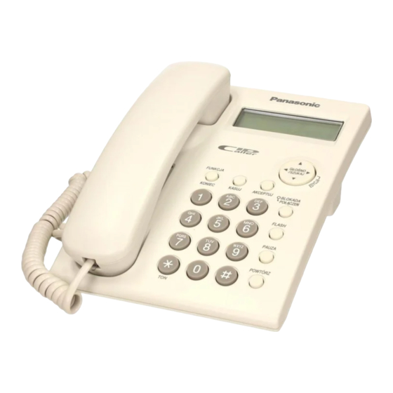
Page 7: Location Of Controls
KX-TSC11AGW 5 LOCATION OF CONTROLS... -
Page 8: Display
KX-TSC11AGW 6 DISPLAY... -
Page 9: Settings
7.1. Connecting the Handset/Telephone Line Cord · Use only a Panasonic Handset for the KX-TSC11AGW. · Use only a telephone line cord included with the unit. · If your unit is connected to a PBX which does not support Caller ID services, you cannot access those services. -
Page 10: Dialing Mode
KX-TSC11AGW 7.2. Dialing Mode... -
Page 11: How To Release The Establishment Of Password
KX-TSC11AGW 7.3. How to Release the Establishment of Password After the following procedure, you will be able to establish a new password. -
Page 12: Call Restriction
KX-TSC11AGW 7.4. Call Restriction For Service Hint: *: If the current password is forgotten, refer to How to Release the Establishment of Password (P.11). -
Page 13: Operations
KX-TSC11AGW 8 OPERATIONS 8.1. Making Calls 8.2. Answering Calls... -
Page 14: For Call Waiting Service Users
KX-TSC11AGW 8.3. For Call Waiting Service Users 8.4. FLASH Button... -
Page 15: Phone Book
KX-TSC11AGW 8.5. Phone Book 8.5.1. Storing Names and Phone Numbers in Phone Book List... - Page 16 KX-TSC11AGW Cross Reference: Erasing (P.21) Chain Dial (P.20)
- Page 17 KX-TSC11AGW...
- Page 18 KX-TSC11AGW 8.5.2. Storing Caller List Information in the Phone Book List Cross Reference: Erasing (P.21)
- Page 19 KX-TSC11AGW 8.5.3. Dialing from the Phone Book...
- Page 20 KX-TSC11AGW 8.5.4. Chain Dial Cross Reference: Dialing from the Phone Book (P.19)
- Page 21 KX-TSC11AGW 8.5.5. Editing Cross Reference: Dialing from the Phone Book (P.19) 8.5.6. Erasing Cross Reference: Dialing from the Phone Book (P.19)
-
Page 22: Troubleshooting
KX-TSC11AGW 9 TROUBLESHOOTING Cross Reference: (*1) Battery Replacement (P.6) (*2) Dialing Mode (P.10) (*3) Call Restriction (P.12) - Page 23 KX-TSC11AGW...
-
Page 24: Disassembly Instructions
KX-TSC11AGW 10 DISASSEMBLY INSTRUCTIONS Shown in Fig —. To remove —. Remove —. Cabinet Cover Screws (2.6 × 12).........(A ) × 4 Main P.C. Board Screws (2.0 × 6)........(B ) × 6 Screws (2.6 × 10).........(C ) × 4... -
Page 25: Troubleshooting Guide
KX-TSC11AGW 11 TROUBLESHOOTING GUIDE Make sure batteries are installed for proper operation before troubleshooting. 11.1. Service Hints 11.2. Pulse Dialing Problems 11.3. Tone Dialing Problems (handset) -
Page 26: No Ringing Sound When Ring Signal Is Input
KX-TSC11AGW 11.4. No Ringing Sound When Ring Signal is Input... -
Page 27: Test Mode
KX-TSC11AGW 12 TEST MODE Note: After the test, the unit will be back to the factory preset mode. -
Page 28: Block Diagram
KX-TSC11AGW... -
Page 29: Circuit Operation
KX-TSC11AGW 14 CIRCUIT OPERATION 14.1. Bell Detector Circuit When the bell signal is input between T/R, the signal are outputted at the speaker via the following path: TEL line → R1/C1 → Pin 8 of IC2 → Pin 5 of IC2 → PC1 → SW1 → Ringer 14.2. - Page 30 KX-TSC11AGW 14.3.2. Initializing Circuit 14.3.2.1. Function This circuit is used to initialize the CPU when the batteries are installed. 14.3.2.2. Circuit operation When the batteries are inserted into the unit, then the voltage is regulated by IC302 and power is supplied to the CPU. The unit...
-
Page 31: Caller Id Detect Circuit
KX-TSC11AGW 14.4. Caller ID Detect Circuit 14.4.1. Function (FSK signal) The caller ID is a chargeable ID which the user of a telephone circuit obtains by entering a contract with the telephone company to utilize a caller ID service. For this reason, the operation of this circuit assumes that a caller ID service contract has been entered for the circuit being used. -
Page 32: Ic Block Diagram
KX-TSC11AGW 15 IC BLOCK DIAGRAM 15.1. IC502... -
Page 33: Cpu Data (Ic502)
KX-TSC11AGW 15.2. CPU DATA (IC502) -
Page 34: Ringer Ic (Ic2)
KX-TSC11AGW 15.3. RINGER IC (IC2) 15.4. EEPROM (IC802) (1) SCK SCK terminal is input terminal of Serial Clock to control transmit and receipt between Master and Slave. (2) SDA SDA terminal is input terminal, to forward the address and the mutual data between Master Device and Slave Device the mutual. -
Page 35: How To Replace Flat Package Ic
KX-TSC11AGW 16 HOW TO REPLACE FLAT PACKAGE IC Even if you do not have the special tools (for example, a spot heater) to remove the Flat IC, with some solder (large amount), a soldering iron and a cutter knife, you can easily remove the ICs that have more than 100 pins. -
Page 36: Flat Package Ic Installation Procedure
KX-TSC11AGW 16.3. FLAT PACKAGE IC INSTALLATION PROCEDURE 1. Temporarily fix the FLAT PACKAGE IC, soldering the two marked pins. *Check the accuracy of the IC setting with the corresponding soldering foil. 2. Apply flux to all pins of the FLAT PACKAGE IC. -
Page 37: Cabinet And Electrical Parts
KX-TSC11AGW 17 CABINET AND ELECTRICAL PARTS Note: *1: Batteries are not included. -
Page 38: Accessories And Packing Materials
KX-TSC11AGW 18 ACCESSORIES AND PACKING MATERIALS... -
Page 39: Terminal Guide Of The Ics, Transistors And Diodes
KX-TSC11AGW 19 TERMINAL GUIDE OF THE ICs, TRANSISTORS AND DIODES... -
Page 40: Replacement Parts List
KX-TSC11AGW 20 REPLACEMENT PARTS LIST 1. RTL (Retention Time Limited) Ref. Part No. Part Name & Description Remarks Note: PQJC10045Z BATTERY TERMINAL (-) The marking (RTL) indicates that the Retention Time is PQJC313Y BATTERY TERMINAL (+) (-) PQJC314Y BATTERY TERMINAL (-) (+) limited for this item. - Page 41 KX-TSC11AGW Ref. Part No. Part Name & Description Remarks Ref. Part No. Part Name & Description Remarks (SWITCHES) R485 ERJ3GEYJ103 PQSS3A17W SWITCH, SLIDE R486 ERJ3GEYJ103 SW101 PQSH2B105Z SWITCH, HOOK R487 ERJ3GEY0R00 (VARIABLE RESISTORS) R520 ERJ3GEYJ105 VR401 PQNVZ6TLTB13 VARIABLE RESISTOR R551...
-
Page 42: Accessories And Packing Materials
KX-TSC11AGW Ref. Part No. Part Name & Description Remarks C504 ECJ1VB1H472K 0.0047 C553 ECUV1C104KBV C555 ECUV1H331JCV 330P C557 ECUV1H103KBV 0.01 C806 ECUV1H150JCV C807 ECUV1H150JCV C808 ECUV1H101JCV 100P C810 ECUV1H223KBV 0.022 C811 ECUV1H681JCV 680P C812 ECUV1C333KBV 0.033 C814 ECEA1CKA100 C815 ECUV1H681JCV... -
Page 43: For Schematic Diagram
KX-TSC11AGW 21 FOR SCHEMATIC DIAGRAM 1. SW101: Hook switch. 2. SW1: Ringer selector. 3. DC voltage measurements are taken with electronic voltmeter from negative voltage line. 4. (Add 40 mA to telephone line from the loop simulator.) 5. Off-hook condition 6. -
Page 44: Schematic Diagram
KX-TSC11AGW 22 SCHEMATIC DIAGRAM TRANSISTOR VOLTAGE CHECK (MAIN PCB) COM0 MODE (TALK) (BELL) COM1 PARTS No. Emitter Collector Base Emitter Collector Base Q102 9.20 9.10 8.54 0.11 0.37 0.10 COM2 Q104 0.00 0.10 0.56 0.00 0.35 0.31 COM3 Q108 4.96 8.50... - Page 45 KX-TSC11AGW VOLTAGE CHECK (IC2) MODE (TALK) (BELL) PIN No. 7.65 32.0(AC) 8.72 23.0(AC) 8.39 23.0(AC) 8.73 23.0(AC) 8.31 24.3(AC) 0.05 0.70(AC) RINGERP 9.35 23.2(AC) 250V1 9.20 14.9(AC) SW101 ONHOOK C402 RINGERM R405 C404 270P R118 Q401 K0.1 R401 C401 15(1/2W )
-
Page 46: Memo
KX-TSC11AGW 22.1. Memo... -
Page 47: Circuit Board
KX-TSC11AGW SA101 POS101 JJ101 L101 L102 C101 J013 R126 X801 C819 J014 J006 C814 J009 Q104 Q103 R106 J010 Q102 Q181 C106 Q106 R114 D105 J004 C420 VR401 YELLOW VR402 VR481 C409 C410 J001... -
Page 48: Flow Solder Side View
KX-TSC11AGW... - Page 49 KX-TSC11AGW I.N./N KXTSC11AGW...