Table of Contents
Advertisement
SERVICE MANUAL
Main Section
I Specifications
I Preparation for Servicing
I Adjustment Procedures
I Schematic Diagrams
I CBA's
I Exploded views
I Parts List
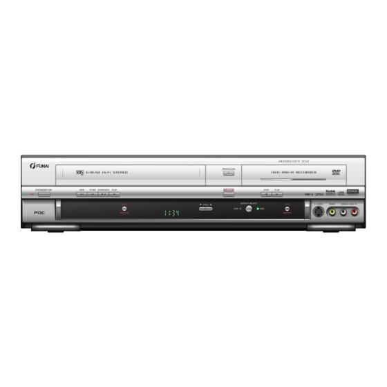
VIDEO CASSETTE RECORDER
DVD RECORDER &
DRVR-B778S
When servicing the deck
mechanism, refer to MK14 Deck
Mechanism Section.
Deck Mechanism Part No.:
N25E0FL
PAL
Advertisement
Table of Contents

Related Manuals for FUNAI DRVR-B778S


Summary of Contents for FUNAI DRVR-B778S
- Page 1 When servicing the deck I Specifications mechanism, refer to MK14 Deck I Preparation for Servicing Mechanism Section. I Adjustment Procedures I Schematic Diagrams Deck Mechanism Part No.: I CBA’s I Exploded views N25E0FL I Parts List DVD RECORDER & VIDEO CASSETTE RECORDER DRVR-B778S...
-
Page 2: Table Of Contents
MAIN SECTION DVD RECORDER & VIDEO CASSETTE RECORDER DRVR-B778S Main Section I Specifications I Preparation for Servicing I Adjustment Procedures I Schematic Diagrams I CBA’s I Exploded Views I Parts List TABLE OF CONTENTS Specifications ............... . . 1-1-1 Laser Beam Safety Precautions . -
Page 3: Specifications
SPECIFICATIONS < VCR Section > Description Unit Minimum Nominal Maximum Remark 1. Video 1-1. Video Output (PB) Vp-p SP Mode 1-2. Video Output (R/P) Vp-p SP Mode, 1-3. Video S/N Y (R/P) W/O Burst 1-4. Video Color S/N AM (R/P) SP Mode 1-5. - Page 4 < DVD Section > Item Conditions Unit Nominal Limit 1. VIDEO 75 Ω load 1-1. Video Output Vp-p 1-2. S-Video Output 75 Ω load Y (Luminance) Vp-p 75 Ω load C (Chrominance) Vp-p 2. AUDIO 2-1. Output Level Vrms 2-2. Frequency Response DVD-VIDEO LPCM fs = 96 kHz 20 - 44 k...
-
Page 5: Laser Beam Safety Precautions
LASER BEAM SAFETY PRECAUTIONS This DVD player uses a pickup that emits a laser beam. Do not look directly at the laser beam coming from the pickup or allow it to strike against your skin. The laser beam is emitted from the location shown in the figure. When checking the laser diode, be sure to keep your eyes at least 30 cm away from the pickup lens when the diode is turned on. -
Page 6: Important Safety Precautions
IMPORTANT SAFETY PRECAUTIONS Product Safety Notice K. When connecting or disconnecting the internal connectors, first, disconnect the AC plug from the Some electrical and mechanical parts have special AC outlet. safety-related characteristics which are often not evi- dent from visual inspection, nor can the protection they give necessarily be obtained by replacing them with components rated for higher voltage, wattage, etc. - Page 7 Safety Check after Servicing Examine the area surrounding the repaired location for damage or deterioration. Observe that screws, Chassis or Secondary Conductor parts, and wires have been returned to their original positions. Afterwards, do the following tests and con- Primary Circuit firm the specified values to verify compliance with safety standards.
-
Page 8: Standard Notes For Servicing
STANDARD NOTES FOR SERVICING Circuit Board Indications Pb (Lead) Free Solder 1. The output pin of the 3 pin Regulator ICs is When soldering, be sure to use the Pb free solder. indicated as shown. How to Remove / Install Flat Pack-IC Top View Bottom View 1. - Page 9 3. The flat pack-IC on the CBA is affixed with glue, so With Soldering Iron: be careful not to break or damage the foil of each 1. Using desoldering braid, remove the solder from pin or the solder lands under the IC when all pins of the flat pack-IC.
- Page 10 2. Installation With Iron Wire: 1. Using desoldering braid, remove the solder from 1. Using desoldering braid, remove the solder from all pins of the flat pack-IC. When you use solder the foil of each pin of the flat pack-IC on the CBA flux which is applied to all pins of the flat pack-IC, so you can install a replacement flat pack-IC more you can remove it easily.
- Page 11 Instructions for Handling Semi- conductors Electrostatic breakdown of the semi-conductors may occur due to a potential difference caused by electrostatic charge during unpacking or repair work. 1. Ground for Human Body Be sure to wear a grounding band (1 MΩ) that is properly grounded to remove any static electricity that may be charged on the body.
-
Page 12: Preparation For Servicing
PREPARATION FOR SERVICING How to Enter the Service Mode About Optical Sensors Caution: An optical sensor system is used for the Tape Start and End Sensors on this equipment. Carefully read and follow the instructions below. Otherwise the unit may operate erratically. What to do for preparation Insert a tape into the Deck Mechanism Assembly and press the [PLAY] (VCR) button. -
Page 13: Cabinet Disassembly Instructions
CABINET DISASSEMBLY INSTRUCTIONS 1. Disassembly Flowchart REMOVAL This flowchart indicates the disassembly steps to gain REMOVE/*UNHOOK/ LOC. PART Fig. access to item(s) to be serviced. When reassembling, UNLOCK/RELEASE/ Note follow the steps in reverse order. Bend, route, and UNPLUG/DESOLDER dress the cables as they were originally. Power [12] Supply... - Page 14 Reference Notes CAUTION 1: Locking Tabs (L-1) and (L-2) are fragile. [4] Jack Bracket Be careful not to break them. (S-4) 1-1. Release five Locking Tabs (L-1). 1-2. Release three Locking Tabs (L-2). 1-3. Disconnect Connector (CN1505), and remove the Front Assembly. 2.
- Page 15 (S-7) (S-8) (S-10) (S-6A) (S-6B) [8] Rear [12] Power Supply Panel Unit (S-7) (S-11) (S-7) [13] PCB Holder CN1503 Fig. D5 CN1504 Fig. D7 [11] Rear Panel (S-12) (S-9) (S-14) (S-14) (S-15) (S-13C) Washer [10] Motor DC Fan [9] Fan Holder Fig.
- Page 16 [15] Deck Cylinder Assembly Assembly FE Head ACE Head Assembly SW507 LD-SW 21P Earth Plate [18] Rear Jack [16] Power [19] Main CBA SW CBA (with AFV CBA) [19] Main CBA [15] Deck Assembly Cam Gear Desolder (S-17) from bottom Hole Shaft (S-18)
- Page 17 (S-19) (S-19) (S-19) (S-19) [20] Deck Pedestal [21] Front Bracket R (S-20) Fig. D10 1-6-5 E9G01DC...
- Page 18 3. How to Eject Manually Note: When rotating the gear, be careful not to damage the gear. 1. Remove the Top Cover. 2. Remove the Front Assembly. 3. Remove the Front Bracket. 4. Remove the DVD Mechanism & DVD Main CBA Assembly. 5.
-
Page 19: Electrical Adjustment Instructions
ELECTRICAL ADJUSTMENT INSTRUCTIONS NOTE: 1.Electrical adjustments are required after replacing circuit components and certain mechanical parts. It is important to do these adjustments only after Figure 1 all repairs and replacements have been com- pleted. Also, do not attempt these adjustments unless the proper equipment is available. -
Page 20: How To Initialize The Dvd Recorder & Vcr
HOW TO INITIALIZE THE DVD RECORDER & VCR To put the program back at the factory-default, initialize the DVD recorder & VCR as the following procedure. < DVD Section > 1. Turn the DVD recorder on. 2. Confirm that no disc is loaded or that the disc tray is open. -
Page 21: Firmware Renewal Mode
FIRMWARE RENEWAL MODE 1. Turn the power on and remove the disc on the tray. 4. Select the firmware version pressing arrow buttons, then press [ENTER]. 2. To put the DVD recorder into version up mode, Fig. d appears on the screen and Fig. e appears press [CM SKIP], [6], [5], and [4] buttons on the on the VFD. -
Page 22: Function Indicator Symbols
FUNCTION INDICATOR SYMBOLS < VCR Section > Note: If a mechanical malfunction occurs, the power is turned off. When the power comes on again after that by pressing [STANDBY-ON] button, an error message is displayed on the TV screen for 5 seconds. MODE INDICATOR ACTIVE When reel or capstan mechanism is not... - Page 23 < DVD Section > Note: If an error occurs, a message with the error number appears on the screen. Recording Error Error message You cannot record on this disc as Power Calibration Area is full. Error No. Error Message Solution Error Description Priority An error occurs during data reading.
- Page 24 Error Message Solution Error Description Priority Release the disc protect This disc is protected and not setting in the Disc Setting Disc Protected Disc. recordable. menu. Disc is full. Insert the recordable disc with No available recording space. (No area for new recording) enough recording space.
-
Page 25: Troubleshooting
TROUBLESHOOTING 1 Power Supply Section FLOW CHART NO.1 The power cannot be turned on. See FLOW CHART No.2 <The fuse blows out.> Is the fuse normal? Is normal state restored when once unplugged Check for lead or short-circuiting of primary power cord is plugged again after several seconds. - Page 26 FLOW CHART NO.6 P-ON+44V is not outputted. Check D013, C013, and their periphery, and Is 44V voltage supplied to the emitter of Q1516? service it if defective. Is the "L" pulse (approximately 0V) inputted to Is the "H" pulse (approximately 5V) inputted to the base of Q1516? the base of Q1517? Replace Q1516.
- Page 27 FLOW CHART NO.11 DVD-P-ON+3.3V is not outputted. Is 5V voltage supplied to Pin(1) of IC1505? Check D015, D016, D1032, L013, C018 and their periphery, and service it if defective. Replace IC1505. FLOW CHART NO.12 DVD-P-ON+12V is not outputted. Is 12V voltage supplied to the emitter of Q1511? Check D1031, L1013, C1037, C1039 and their periphery, and service it if defective.
- Page 28 2 DVD Section FLOW CHART NO.1 The key operation is not functioning. Are the contact point and the installation state of Re-install the key switches correctly or replace the key switches normal? the poor switch. Is the control voltage normally inputted into Pin(8) Check the key switches and their periphery, and service it if defective.
- Page 29 FLOW CHART NO.4 VIDEO E-E does not appear normally. Are the video signals inputted to each pin of Check the line between video input terminal and IC1518? each pin of IC1518. IC1518 1PIN VIDEO-IN1 (AV1) 1PIN → JK1502 VIDEO-IN1 (AV1) IC1581 IC1518 3PIN...
- Page 30 FLOW CHART NO.5 Picture does not appear normally. [In the S-VIDEO/Composite video output (JK1502, JK1506, JK2001)] Set the disc on the disc tray and playback. "A" Replace DVD MECHANISM & DVD MAIN CBA Are the video signals inputted to each pin of CN1502? No ASSEMBLY.
- Page 31 FLOW CHART NO.6 Picture does not appear normally. [In the RGB/Component video output (JK1501, JK1502)] Set the disc on the disc tray and playback. "B" Are the video signals outputted to each pin of Replace DVD MECHANISM & DVD MAIN CBA CN1502? ASSEMBLY.
- Page 32 "C1" Check the line between each pin of IC1516 and Are the video signals inputted to each pin of IC1516 each pin of IC1510, and service it if defective. and each pin of IC1514? IC1516 3PIN → IC1510 13PIN VIDEO-Y(I/P)-OUT (Output to JK1501) IC1516 8PIN →...
- Page 33 FLOW CHART NO.7 Audio E-E does not appear normally. Check the line between audio input terminal and each pin of IC1518, and service it if defective. No (Rear Are the audio signals inputted to each pin of input) →JK1502 IC1518 10,16PIN AUDIO-IN1 (AV1) IC1518?
- Page 34 "C" Check each line between each pin of CN1502 Are the analog audio signals inputted to each pin and each pin of IC1513, and service it if defective. of IC1513? CN1502 17PIN → IC1513 2PIN AUDIO(L)-OUT IC1513 2PIN AUDIO (L)-OUT CN1502 15PIN →...
- Page 35 FLOW CHART NO.8 Audio is not outputted during playback. Set the disc on the disc tray, and playback. Replace the DVD MECHANISM & DVD MAIN Are the analog audio signals outputted to each pin CBA ASSEMBLY. of CN1502? CN1502 17PIN AUDIO (L)-OUT CN1502 15PIN AUDIO (R)-OUT Check each line between each pin of CN1502 Are the analog audio signals inputted to each pin...
- Page 36 "D" Are the analog audio signals outputted to each pin of IC1518? Is 12V voltage supplied to Pin(2,4) of IC1518? IC1518 21,25PIN AUDIO-OUT 1 (AV1) IC1518 22,26PIN AUDIO-OUT 2 (AV2) Check the AL+12V line and Replace IC1518. service it if defective. Are the audio signals outputted to the specific Check the periphery between Pin(21,25) of IC1518 output terminal?
- Page 37 3 VCR Section FLOW CHART NO.1 The key operation is not functioning. Are the contact point and the installation state of Re-install some key switches correctly or the key switches normal? replace some key switches. Check the key switches and their periphery, and Is the control voltage normally inputted into service it if defective.
- Page 38 FLOW CHART NO.3 Cassette tape can not be loaded. When loading a cassette tape, on Pin(10) of Check the line between the start sensor and IC501, does the "L" pulse switch to the "H" pulse? Pin(10) of IC501, and service it if defective. When loading a cassette tape, is the specified Replace the Capstan Motor Unit.
- Page 39 FLOW CHART NO.6 Capstan Motor does not rotate. Is 5V voltage supplied to Pin(2) of CN502? Check the P-ON+5V line and service it if defective. Is over approximately 2.6V voltage supplied to Check the line between Pin(5) of CN502 and Pin(5) of CN502? Pin(76) of IC501, and service it if defective.
- Page 40 FLOW CHART NO.10 Video E-E does not appear. Are the video signals inputted to each pin of Check the line between video input terminal and IC1518? each pin of IC1518. IC1518 1PIN VIDEO-IN1 (AV1) 1PIN → JK1502 VIDEO-IN1 (AV1) IC1581 3PIN →...
- Page 41 "E" Are the video signals outputted to each pin of IC1518? Is 12V voltage supplied to Pin(2,4) of IC1518? IC1518 29PIN VIDEO-OUT 1 (AV1) IC1518 30PIN VIDEO-OUT 2 (AV2) Check the AL+12V(1) line Replace IC1518. and service it if defective. Are the video signals outputted to the specific output terminal? Check the periphery of JK1502 from Pin(29) of...
- Page 42 "F" Check the line between Pin(3,13) of IC1501 and Is the audio signal supplied to Pin(4,50) of IC451? Pin(4,50) of IC451, and service it if defective. Is the 5V voltage supplied to Pin(16,32,35,36,46,55) of Check the circuit of AL+5V(1), P-ON+5V and IC451, or the 9V voltage supplied to Pin(69) of IC451? P-ON+9V, and service it if defective.
- Page 43 FLOW CHART NO.12 Hi-Fi audio can not be recorded normally. (E-E mode is normal.) Is the REC FM signal outputted to Pin(26) of IC451? Replace IC451. Check the line between Pin(8) of CN251 and Is the REC FM signal outputted to Pin(8) of CN251? Pin(26) of IC451, and service it if defective.
- Page 44 FLOW CHART NO.15 Hi-Fi audio can not be playbacked normally in the linear audio mode. (E-E mode is normal.) Is the audio signal outputted to Pin(11) of IC301? Is the audio signal supplied to Pin(5) of IC301? Check the line between Pin(11) of Replace IC301 and Pin(80) of IC451, and IC301.
-
Page 45: Block Diagrams
BLOCK DIAGRAMS Servo/System Control Block Diagram 1-12-1 E9G01BLS... - Page 46 Digital Signal Process Block Diagram 1-12-2 E9G01BLD...
- Page 47 Video Block Diagram 1-12-3 E9G01BLV...
- Page 48 Video Input Select Block Diagram 1-12-4 E9G01BLVIS...
- Page 49 Video Output Select Block Diagram E9G01BLVOS 1-12-5...
- Page 50 Audio Block Diagram E9G01BLA 1-12-6...
- Page 51 Audio Input/Output Select Block Diagram E9G01BLAS 1-12-7...
- Page 52 Hi-Fi Audio Block Diagram 1-12-8 E9G01BLH...
- Page 53 Power Supply Block Diagram 1-12-9 E9G01BLP...
-
Page 54: Schematic Diagrams / Cba's And Test Points
SCHEMATIC DIAGRAMS / CBA’S AND TEST POINTS Standard Notes WARNING Many electrical and mechanical parts in this chassis have special characteristics. These characteristics often pass unnoticed and the protection afforded by them cannot necessarily be obtained by using replacement components rated for higher voltage, wattage, etc. - Page 55 LIST OF CAUTION, NOTES, AND SYMBOLS USED IN THE SCHEMATIC DIAGRAMS ON THE FOLLOWING PAGES: 1. CAUTION: FOR CONTINUED PROTECTION AGAINST FIRE HAZARD, REPLACE ONLY WITH THE SAME TYPE FUSE. 2. CAUTION: Fixed Voltage (or Auto voltage selectable) power supply circuit is used in this unit. If Main Fuse (F1001) is blown, first check to see that all components in the power supply circuit are not defective before you connect the AC plug to the AC power supply.
- Page 56 Main 1/9 Schematic Diagram < VCR Section > 1-13-3 E9G10SCM1...
- Page 57 Main 2/9, Power SW, Function & Sensor Schematic Diagram < VCR Section > FL601 MATRIX CHART P.SCAN REPEAT VCD VCR VCD VCR XP SP LP EP REPEAT P.SCAN 1-13-4 E9G10SCM2...
- Page 58 Main 3/9 Schematic Diagram < VCR Section > 1-13-5 E9G10SCM3...
- Page 59 Main 4/9 Schematic Diagram < VCR Section > 1-13-6 E9G10SCM4...
- Page 60 Main 5/9 Schematic Diagram < VCR Section > 1-13-7 E9G10SCM5...
- Page 61 Main 6/9 & Front Jack Schematic Diagram < VCR Section > 1-13-8 E9G10SCM6...
- Page 62 Main 7/9 Schematic Diagram < VCR Section > 1-13-9 E9G10SCM7...
- Page 63 Main 8/9 Schematic Diagram < VCR Section > E9G10SCM8 1-13-10...
- Page 64 Main 9/9 Schematic Diagram < VCR Section > E9G10SCM9 1-13-11...
- Page 65 Power Supply Schematic Diagram < VCR Section > CAUTION ! CAUTION ! NOTE: Fixed voltage (or Auto voltage selectable) power supply circuit is used in this unit. For continued protection against fire hazard, The voltage for parts in hot circuit is measured using If Main Fuse (F1001) is blown , check to see that all components in the power supply replace only with the same type fuse.
- Page 66 Rear Jack Schematic Diagram < VCR Section > E9G10SCRJ 1-13-13...
- Page 67 AFV Schematic Diagram < VCR Section > E9G10SCAFV 1-13-14...
- Page 68 DVD Main 1/5 Schematic Diagram < DVD Section > 1 NOTE: The order of pins shown in this diagram is different from that of actual IC101. IC101 is divided into five and shown as IC101 (1/5) ~ IC101 (5/5) in this DVD Main Schematic Diagram Section. 1-13-15 E9G10SCD1...
- Page 69 DVD Main 2/5 Schematic Diagram < DVD Section > 1 NOTE: The order of pins shown in this diagram is different from that of actual IC101. IC101 is divided into five and shown as IC101 (1/5) ~ IC101 (5/5) in this DVD Main Schematic Diagram Section. 1-13-16 E9G10SCD2...
- Page 70 DVD Main 3/5 Schematic Diagram < DVD Section > 1 NOTE: The order of pins shown in this diagram is different from that of actual IC101. IC101 is divided into five and shown as IC101 (1/5) ~ IC101 (5/5) in this DVD Main Schematic Diagram Section. 1-13-17 E9G10SCD3...
- Page 71 DVD Main 4/5 Schematic Diagram < DVD Section > 1 NOTE: The order of pins shown in this diagram is different from that of actual IC101. IC101 is divided into five and shown as IC101 (1/5) ~ IC101 (5/5) in this DVD Main Schematic Diagram Section. 1-13-18 E9G10SCD4...
- Page 72 DVD Main 5/5 Schematic Diagram < DVD Section > 1 NOTE: The order of pins shown in this diagram is different from that of actual IC101. IC101 is divided into five and shown as IC101 (1/5) ~ IC101 (5/5) in this DVD Main Schematic Diagram Section. 1-13-19 E9G10SCD5...
- Page 73 Main CBA Top View Sensor CBA Top View BHF300F01012A J236 JK1-V-OUT BHF300F01012B TP301 C-PB VR501 SW-POINT TP503 TP504 RF-SW TP501 S-INH 1-13-20 BE9G00F01012A...
- Page 74 Main CBA Bottom View PIN 17 OF PIN 9 OF PIN 7 OF PIN 5 OF PIN 3 OF PIN 6 OF CN1502 CN1502 CN1502 CN1502 CN1502 IC1515 WF10 PIN 3 OF CN1501 1-13-21 BE9G00F01012A...
- Page 75 Power SW CBA Top View Power SW CBA Bottom View BE9G00F01012B Function CBA Top View Function CBA Bottom View Front Jack CBA Top View Front Jack CBA Bottom View BE9G00F01012D BE9G00F01012C 1-13-22...
- Page 76 Power Supply CBA Top View CAUTION ! CAUTION ! Because a hot chassis ground is present in the power For continued protection against fire hazard, Fixed voltage (or Auto voltage selectable) power supply circuit is used in this unit. supply circut, an isolation transformer must be used. If Main Fuse (F1001) is blown , check to see that all components in the power supply Also, in order to have the ability to increase the input replace only with the same type fuse.
- Page 77 Power Supply CBA Bottom View CAUTION ! CAUTION ! Because a hot chassis ground is present in the power For continued protection against fire hazard, Fixed voltage (or Auto voltage selectable) power supply circuit is used in this unit. supply circut, an isolation transformer must be used. If Main Fuse (F1001) is blown , check to see that all components in the power supply Also, in order to have the ability to increase the input replace only with the same type fuse.
- Page 78 REAR JACK CBA Bottom View REAR JACK CBA Top View BE9B00F01022B AFV CBA Top View AFV CBA Bottom View BE6800F01091 1-13-25...
-
Page 79: Waveforms
WAVEFORMS NOTE: Input: COLOR BAR SIGNAL (WITH 1KHz AUDIO SIGNAL) TP301 UPPER Pin 3 of CN1502 TP504 Pin 6 of IC1515 LOWER C-PB 0.2V RF-SW VIDEO-Cb 0.2V 20µs VIDEO-CVBS 0.5V 20µs J236 UPPER Pin 7 of CN1502 Pin 3 of CN1501 TP504 WF10 LOWER... -
Page 80: Wiring Diagram < Vcr Section
WIRING DIAGRAM < VCR SECTION > 1-15-1 E9G01WI... -
Page 81: Wiring Diagram < Dvd Section
WIRING DIAGRAM < DVD SECTION > DVD/CD LASER DIODE DRIVE E9G01WID 1-15-2... -
Page 82: Ic Pin Function Descriptions
IC PIN FUNCTION DESCRIPTIONS < VCR Section > Signal Function Name IC501( SERVO / SYSTEM CONTROL ) AUDIO- 28 OUT Audio Mute Control Signal MUTE-2 Signal DVD- Function Name DVD Audio Mute Control 29 OUT AUDIO- Signal MUTE2 Input Signal from Pin 8 of IN SC2-IN SCART2 DVD-... - Page 83 Signal Signal Function Function Name Name DVD-POW- DVD Power Supply Safety Control SCART 1 8Pin Level 59 OUT 8POUT-1 SAFETY Signal by using 8POUT-1 and 8POUT-2 IN D-PFG Drum PG/FG Input Signal Control SCART 1 8Pin Level AMPVREF 60 OUT 8POUT-2 by using 8POUT-1 and V-Ref for CTL AMP 8POUT-2...
- Page 84 IC612 ( VFD DRIVER ) Signal Name Function Name Signal Name Function Name POWER- Power LED Control Signal OUT DVD-LED DVD LED Control Signal Grid Output OUT VCR-LED VCR LED Control Signal Not Used Oscillator Input Not Used +5V Power Supply DRV-DIN DRV-Serial Data Ground...
-
Page 85: Lead Identifications
LEAD IDENTIFICATIONS KRA103M-AT/P 2SA1015-GR(TE2 F T) PQ070XF01SZH 2SK3566 KRA104M-AT/P 2SA1020-Y(TE6 F M) PQ070XFC1SZF KRC103M-AT/P 2SC1815-(BL,GR,Y)(TE2 F T) KTA1267-(GR,Y)-AT/P 2SC2120-Y(TE2 F T) KTA1273-Y-AT/P 2SC3266-Y(TPE2 F) KTA1281Y-AT/P KTA-1266-GR-AT/P KTC3199-(BL,GR,Y)-AT/P KTC3198-(GR,Y)-AT/P RN1203(TE4 F T) KTC3203-Y-AT/P RN2203(TE4 F T) KTC3205-Y-AT/P RN2204(TE4 F T) 1 2 3 4 G D S E C B E C B... -
Page 86: Exploded Views
EXPLODED VIEWS Cabinet JW102 See Electrical Parts List 2L011 for parts with this mark. 2L011 2L071 JW101 2L071 2L071 2L071 DVD MECHANISM & DVD 2L111 MAIN CBA ASSEMBLY 2L111 2L111 2B60 TU1501 AFV CBA 2B76 2L033 2B77 2L081 Rear Jack CBA 2L111 2L082 Sensor CBA... - Page 87 Packing 1-18-2 E9G01PEX...
-
Page 88: Mechanical Parts List
MECHANICAL PARTS LIST PRODUCT SAFETY NOTE: Products marked with a Ref. No. Description Part No. ! have special characteristics important to safety. DRY BATTERY R6P/2S or XB0M451T0001 Before replacing any of these components, read DRY BATTERY ES-GR6M-C or XB0M571GLP01 carefully the product safety notice in this service DRY BATTERY R6UW/2S XB0M311MS001 manual. -
Page 89: Electrical Parts List
ELECTRICAL PARTS LIST PRODUCT SAFETY NOTE: Products marked with a Ref. No. Description Part No. ! have special characteristics important to safety. C317 CHIP CERAMIC CAP .(1608) F Z 0.1µF/50V CHD1JZ30F104 Before replacing any of these components, read C322 CHIP CERAMIC CAP .(1608) F Z 0.1µF/50V CHD1JZ30F104 carefully the product safety notice in this service C324... - Page 90 Ref. No. Description Part No. Ref. No. Description Part No. CAP ELECTROLYTIC 22µF/10V/M/H7 CA1A220ENE10 C519 CHIP CERAMIC CAP . CH J 560pF/50V CHD1JJ3CH561 C454 CHIP CERAMIC CAP .(1608) F Z 0.1µF/50V CHD1JZ30F104 C520 CHIP CERAMIC CAP .(1608) B K 1000pF/50V CHD1JK30B102 C455 CHIP CERAMIC CAP .(1608) F Z 0.1µF/50V...
- Page 91 Ref. No. Description Part No. Ref. No. Description Part No. C1521 CHIP CERAMIC CAP . F Z 1µF/10V CHD1AZ30F105 CAP ELECTROLYTIC 10µF/16V/M CA1C100ENE12 C1524 CHIP CERAMIC CAP .(1608) B K 0.1µF/25V CHD1EK30B104 C1573 ELECTROLYTIC CAP . 10µF/16V M or CE1CMASDL100 C1525 CHIP CERAMIC CAP .(1608) B K 0.01µF/50V CHD1JK30B103...
- Page 92 Ref. No. Description Part No. Ref. No. Description Part No. C1616 ELECTROLYTIC CAP . 470µF/6.3V M or CE0KMASDL471 CAP ELECTROLYTIC 4.7µF/25V/M CA1E4R7ENE12 CAP ELECTROLYTIC 470µF/6.3V/M CA0K471ENE12 C1688 ELECTROLYTIC CAP . 1µF/50V M or CE1JMASDL1R0 C1617 CHIP CERAMIC CAP .(1608) B K 0.1µF/25V CHD1EK30B104 CAP ELECTROLYTIC 1µF/50V/M CA1J1R0ENE12...
- Page 93 Ref. No. Description Part No. Ref. No. Description Part No. D1508 ZENER DIODE MTZJT-774.3C or QDTC0MTZJ4R3 DIODE ZENER 11BSA-T26 or NDTA011BST26 DIODE ZENER 4V3BSC-T26 or NDTC4R3BST26 ZENER DIODE DZ-11BSAT265 NDTA00DZ11BS ZENER DIODE DZ-4.3BSCT265 NDTC0DZ4R3BS D1548 ZENER DIODE MTZJT-7711A or QDTA00MTZJ11 D1511 ZENER DIODE MTZJT-7710B or QDTB00MTZJ10...
- Page 94 Ref. No. Description Part No. Ref. No. Description Part No. L1508 INDUCTOR 10µH-K-26T LLAXKATTU100 TRANSISTOR 2SC1815-GR(TE2 F T) QQS12SC1815F L1509 INDUCTOR(100µH K) LAP02TA101K LLAXKATTU101 Q1515 TRANSISTOR KTC3199-Y-AT/P or NQSYKTC3199P L1510 RADIAL TYPE CHOKE COIL CW68-470K- LLBD00PKV023 TRANSISTOR KTC3199-GR-AT/P or NQS4KTC3199P 841040NP or TRANSISTOR 2SC1815-Y(TE2 F T) or QQSY2SC1815F...
- Page 95 Ref. No. Description Part No. Ref. No. Description Part No. CHIP RES. 1/10W J 5.6k Ω or CHIP RES. 1/10W J 120 Ω or R303 RRXAJR5Z0562 R412 RRXAJR5Z0121 RES CHIP 1608 1/10W J 5.6k Ω RES CHIP 1608 1/10W J 120 Ω RRXA562YF002 RRXA121YF002 CHIP RES.
- Page 96 Ref. No. Description Part No. Ref. No. Description Part No. CARBON RES. 1/4W G 10k Ω RES CHIP 1608 1/10W J 470 Ω RCX4GATZ0103 RRXA471YF002 CARBON RES. 1/6W G 470 Ω or CARBON RES. 1/4W J 10k Ω R516 RCX6GATZ0471 R595 RCX4JATZ0103 CARBON RES.
- Page 97 Ref. No. Description Part No. Ref. No. Description Part No. RES CHIP 1608 1/10W J 4.7k Ω RES CHIP 1608 1/10W J 33k Ω RRXA472YF002 RRXA333YF002 CARBON RES. 1/6W J 2.7k Ω or CHIP RES. 1/10W F 15k Ω or R655 RCX6JATZ0272 R1556...
- Page 98 Ref. No. Description Part No. Ref. No. Description Part No. RES CHIP 1608 1/10W J 6.8k Ω RES CHIP 1608 1/10W J 10k Ω RRXA682YF002 RRXA103YF002 CHIP RES. 1/10W J 150 Ω or CARBON RES. 1/6W J 15k Ω or R1597 RRXAJR5Z0151 R1643...
- Page 99 Ref. No. Description Part No. Ref. No. Description Part No. CHIP RES. 1/10W J 1k Ω or R1689 RRXAJR5Z0102 SW521 TACT SWITCH SKQSAF001A or SST0101AL041 RES CHIP 1608 1/10W J 1.0k Ω RRXA102YF002 TACT SWITCH KSM0614B or SST0101HH013 CHIP RES. 1/10W J 1k Ω or R1690 RRXAJR5Z0102 TACT SWITCH TC-1104(H=9.5)
- Page 100 POWER SW CBA SENSOR CBA Ref. No. Description Part No. Ref. No. Description Part No. POWER SW CBA (MCV-B) ---------- SENSOR CBA 1VSA11699 Consists of the following: Consists of the following: DIODE TRANSISTORS D671 LED(RED) 204HD/E NPQZ00204HDE Q503 PHOTO TRANSISTOR PT204-6B-12 or NPWZT2046B12 SWITCHES PHOTO TRANSISTOR MID-32A22F...
- Page 101 Ref. No. Description Part No. Ref. No. Description Part No. CAP ELECTROLYTIC 100µF/35V/M CA1G101ENE12 DIODE SWITCHING 1N4148-F0021 or NDTZ01N4148F C2014 CERAMIC CAP . B K 0.01µF/500V CCD2JKP0B103 SWITCHING DIODE 1N4148M NDTZ01N4148M DIODES D1030 SCHOTTKY BARRIER DIODE SB240-B/P or NDQZ000SB240 DIODE SCHOTTKY SB240 or NDLZ00SB240S D013 RECTIFIER DIODE BA158 or...
- Page 102 Ref. No. Description Part No. Ref. No. Description Part No. CARBON RES. 1/4W J 4.7k Ω RCX4JATZ0472 ZENER DIODE DZ-11BSAT265 NDTA00DZ11BS CARBON RES. 1/6W G 2.2k Ω or R1023 RCX6GATZ0222 D2002 ZENER DIODE MTZJT-7711A or QDTA00MTZJ11 CARBON RES. 1/4W G 2.2k Ω RCX4GATZ0222 DIODE ZENER 11BSA-T26 or NDTA011BST26...
- Page 103 Ref. No. Description Part No. CHIP CERAMIC CAP . CH J 56pF/50V CHD1JJ3CH560 CHIP CERAMIC CAP .(1608) CH J 22pF/50V CHD1JJ3CH220 CHIP CERAMIC CAP . CH J 56pF/50V CHD1JJ3CH560 CHIP CERAMIC CAP . CH C 3pF/50V or CHD1JC3CH3R0 CHIP CERAMIC CAP . CJ C 3pF/50V or CHD1JC3CJ3R0 CHIP CERAMIC CAP .
- Page 104 DRVR-B778S E9G10BD 2007-07-23...