Table of Contents
Advertisement
Quick Links
Advertisement
Table of Contents

Related Manuals for FUNAI DR-A2601


Summary of Contents for FUNAI DR-A2601
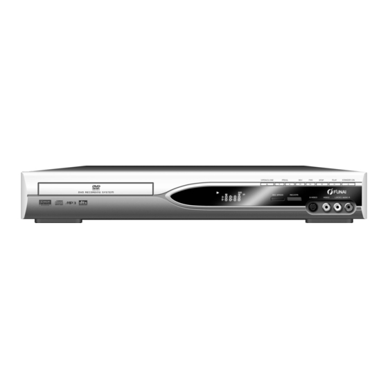
- Page 1 SERVICE MANUAL DVD RECORDER DR-A2601 DR-A2657 DR-A2611...
-
Page 2: Table Of Contents
TABLE OF CONTENTS Specifications ................1-1-1 Laser Beam Safety Precautions . -
Page 3: Specifications
SPECIFICATIONS Item Conditions Unit Nominal Limit 1. VIDEO 75 Ω load 1-1. Video Output Vp-p 1-2. S-Video Output 75 Ω load Y (Luminance) Vp-p 75 Ω load C (Chrominance) Vp-p 2. AUDIO 2-1. Output Level Vrms 2-2. Frequency Response DVD-VIDEO LPCM fs = 96 kHz 20 - 44 k fs = 48 kHz... -
Page 4: Laser Beam Safety Precautions
LASER BEAM SAFETY PRECAUTIONS This DVD player uses a pickup that emits a laser beam. Do not look directly at the laser beam coming from the pickup or allow it to strike against your skin. The laser beam is emitted from the location shown in the figure. When checking the laser diode, be sure to keep your eyes at least 30 cm away from the pickup lens when the diode is turned on. -
Page 5: Important Safety Precautions
IMPORTANT SAFETY PRECAUTIONS Product Safety Notice K. Crimp type wire connector The power transformer uses crimp type connectors Some electrical and mechanical parts have special which connect the power cord and the primary side safety-related characteristics which are often not evi- of the transformer. - Page 6 Safety Check after Servicing Examine the area surrounding the repaired location for damage or deterioration. Observe that screws, Chassis or Secondary Conductor parts, and wires have been returned to their original positions. Afterwards, do the following tests and con- Primary Circuit Terminals firm the specified values to verify compliance with safety standards.
-
Page 7: Standard Notes For Servicing
STANDARD NOTES FOR SERVICING Circuit Board Indications Pb (Lead) Free Solder When soldering, be sure to use the Pb free solder. 1. The output pin of the 3 pin Regulator ICs is indi- cated as shown. How to Remove / Install Flat Pack-IC Top View Bottom View 1. - Page 8 3. The flat pack-IC on the CBA is affixed with glue, so With Soldering Iron: be careful not to break or damage the foil of each (1) Using desoldering braid, remove the solder from all pin or the solder lands under the IC when removing pins of the flat pack-IC.
- Page 9 2. Installation (4) Bottom of the flat pack-IC is fixed with glue to the CBA; when removing entire flat pack-IC, first apply (1) Using desoldering braid, remove the solder from soldering iron to center of the flat pack-IC and heat the foil of each pin of the flat pack-IC on the CBA up.
- Page 10 Instructions for Handling Semi-conductors Electrostatic breakdown of the semi-conductors may occur due to a potential difference caused by electro- static charge during unpacking or repair work. 1. Ground for Human Body Be sure to wear a grounding band (1MΩ) that is prop- erly grounded to remove any static electricity that may be charged on the body.
-
Page 11: Cabinet Disassembly Instructions
[8] Fan Cover D5 2(S-7) [11] AV CBA [9] Fan D5 Fan Earth, *CN1202 --- [12] Jack CBA [13] AFV CBA (S-8), 7(S-9)---[DR-A2601/ [10] Rear Panel DR-A2611] 8(S-9)---[DR-A2657] [11] AV CBA D6 3(S-10) [12] Jack CBA D6 Desolder [13] AFV CBA D6 Desolder ↓... - Page 12 (S-5) [6] Power Supply CBA (S-5) [1] Top Cover (S-4) (S-1) [4] SW CBA (S-1) Desolder (S-6) (S-3) [5] PCB CN1201 Holder (S-1) [7] Power Holder Fig. D4 Fig. D1 [8] Fan Cover (S-7) Fan Earth [2] Front [9] Fan [10] Rear Panel Assembly [DR-A2657] only...
- Page 13 3. How to Eject Manually < Method 1 > Note: When servicing, do not touch white resin part as shown below. When rotating the gear, be careful not to damage the gear. 1. Remove the Top Cover. 2. Rotate the gear in the direction of the arrow manually as shown below. View for A Do not touch! Rotate this gear in...
- Page 14 < Method 2 > Note: When servicing, do not touch white resin part 4. Release the other side of two Locking Tabs, and as shown below. remove the Clamper Assembly. 1. Remove the Top Cover, the Front Assembly and the DVD Mechanism & DVD Main CBA Assembly. Clamper Assembly Then, remove the DVD Mechanism Unit.
-
Page 15: How To Initialize The Dvd Recorder
HOW TO INITIALIZE THE DVD RECORDER To put the program back at the factory-default, initialize the DVD recorder as the following procedure. 1. Turn the DVD recorder on. 2. Confirm that no disc is loaded or that the disc tray is open. -
Page 16: Firmware Renewal Mode
FIRMWARE RENEWAL MODE 1. Turn the power on and remove the disc on the tray. 4. Select the firmware version pressing arrow buttons, then press [ENTER]. 2. To put the DVD recorder into version up mode, Fig. d appears on the screen and Fig. e appears press [CM SKIP], [6], [5], and [4] buttons on the on the VFD. - Page 17 5. After updating is finished, the tray opens automatically. Fig. f appears on the screen and Fig. g appears on the VFD. * Firmware Version differs depending on the models, and this indication is one example. Firm Update Mode ver. R2E2972S2S R2E2972S2S B/E Firmware Update End...
-
Page 18: Function Indicator Symbols
FUNCTION INDICATOR SYMBOLS Note: If an error occurs, a message with the error number appears on the screen. Recording Error Error message You cannot record on this disc as Power Calibration Area is full. Error No. Error Message Solution Error Description Priority An error occurs during data reading. - Page 19 Error Message Solution Error Description Priority Release the disc protect This disc is protected and not setting in the Disc Setting Disc Protected Disc. recordable. menu. Disc is full. Insert the recordable disc with There is no it in a space field. (No area for new recording) enough recording space.
-
Page 20: Block Diagrams
BLOCK DIAGRAMS System Control Block Diagram E6820BLS 1-9-1... - Page 21 Digital Signal Process Block Diagram E6820BLD 1-9-2...
- Page 22 Video Input Select Block Diagram E6820BLVIS 1-9-3...
- Page 23 Video Output Select Block Diagram E6820BLVOS 1-9-4...
- Page 24 Audio Block Diagram E6820BLA 1-9-5...
- Page 25 Power Supply Block Diagram E6820BLP 1-9-6...
-
Page 26: Schematic Diagrams / Cba's And Test Points
SCHEMATIC DIAGRAMS / CBA’S AND TEST POINTS Standard Notes WARNING Many electrical and mechanical parts in this chassis have special characteristics. These characteristics often pass unnoticed and the protection afforded by them cannot necessarily be obtained by using replacement components rated for higher voltage, wattage, etc. - Page 27 LIST OF CAUTION, NOTES, AND SYMBOLS USED IN THE SCHEMATIC DIAGRAMS ON THE FOLLOWING PAGES: 1. CAUTION: FOR CONTINUED PROTECTION AGAINST FIRE HAZARD, REPLACE ONLY WITH THE SAME TYPE FUSE. 2. CAUTION: Fixed Voltage (or Auto voltage selectable) power supply circuit is used in this unit. If Main Fuse (F1001) is blown, first check to see that all components in the power supply circuit are not defective before you connect the AC plug to the AC power supply.
- Page 28 DVD Main 1/6 Schematic Diagram E6820SCD1 1-10-3...
- Page 29 DVD Main 2/6 Schematic Diagram E6820SCD2 1-10-4...
- Page 30 DVD Main 3/6 Schematic Diagram E6820SCD3 1-10-5...
- Page 31 DVD Main 4/6 Schematic Diagram NOTE: 1. The order of pins shown in this diagram is different from that of actual IC601. 2. IC601 is divided into six and shown as IC601 (1/6) ~ IC601 (6/6) in this DVD Main Schematic Diagram Section. 1-10-6 E6820SCD4...
- Page 32 DVD Main 5/6 Schematic Diagram NOTE: 1. The order of pins shown in this diagram is different from that of actual IC601. 2. IC601 is divided into six and shown as IC601 (1/6) ~ IC601 (6/6) in this DVD Main Schematic Diagram Section. E6820SCD5 1-10-7...
- Page 33 DVD Main 6/6 Schematic Diagram NOTE: 1. The order of pins shown in this diagram is different from that of actual IC601. 2. IC601 is divided into six and shown as IC601 (1/6) ~ IC601 (6/6) in this DVD Main Schematic Diagram Section. E6820SCD6 1-10-8...
- Page 34 Group A with the ones under Group B. You can choose either Group. The difference between Group A and Group B is shown below. Group A Group B IC1206 BU4219G-TR PST3619NR C1225 0.015 Comparison Chart of Models and Marks MODEL MARK DR-A2601 DR-A2657 DR-A2611 E6820SCAV1 1-10-9...
- Page 35 AV 2/6 Schematic Diagram FL1203 MATRIX CHART P.SCAN VCD VCR VCD VCR XP SP REPEAT LP EP P.SCAN REPEAT E6820SCAV2 1-10-10...
- Page 36 AV 3/6 Schematic Diagram Comparison Chart of Models and Marks MODEL MARK DR-A2601 DR-A2657 DR-A2611 E6820SCAV3 1-10-11...
- Page 37 AV 4/6 Schematic Diagram E6820SCAV4 1-10-12...
- Page 38 AV 5/6 Schematic Diagram Comparison Chart of Models and Marks MODEL MARK DR-A2601 DR-A2657 DR-A2611 E6820SCAV5 1-10-13...
- Page 39 AV 6/6 Schematic Diagram E6820SCAV6 1-10-14...
- Page 40 Power supply & Junction Schematic Diagram CAUTION ! CAUTION ! Fixed voltage (or Auto voltage selectable) power supply circuit is used in this unit. NOTE: For continued protection against fire hazard, The voltage for parts in hot circuit is measured using If Main Fuse (F1001) is blown , check to see that all components in the power supply hot GND as a common terminal.
- Page 41 AFV Schematic Diagram E6820SCAFV 1-10-16...
- Page 42 Jack Schematic Diagram SW Schematic Diagram E6820SCJ E6820SCSW 1-10-17...
- Page 43 AV CBA Top View 1-10-18 BE6800F01011A...
- Page 44 AV CBA Bottom View C1407 PLUS LEAD PIN 1 OF CN1203 PIN 1 OF CN1204 PIN 3 OF CN1204 PIN 5 OF CN1204 PIN 7 OF CN1204 PIN 9 OF CN1204 PIN 17 OF CN1204 1-10-19 BE6800F01011A...
- Page 45 Power supply CBA Top View CAUTION ! Because a hot chassis ground is present in the power CAUTION ! supply circut, an isolation transformer must be used. For continued protection against fire hazard, Fixed voltage (or Auto voltage selectable) power supply circuit is used in this unit. Also, in order to have the ability to increase the input replace only with the same type fuse.
- Page 46 Power supply CBA Bottom View Because a hot chassis ground is present in the power CAUTION ! CAUTION ! supply circut, an isolation transformer must be used. For continued protection against fire hazard, Fixed voltage (or Auto voltage selectable) power supply circuit is used in this unit. Also, in order to have the ability to increase the input replace only with the same type fuse.
- Page 47 SW CBA Top View SW CBA Bottom View BE6800F01011B Jack CBA Top View Jack CBA Bottom View Junction CBA Junction CBA Bottom View Top View BE6800F01021C BE6800F01021B 1-10-22...
- Page 48 AFV CBA Bottom View AFV CBA Top View 1-10-23 BE6800F01091...
-
Page 49: Waveforms
WAVEFORMS NOTE: Input: COLOR BAR SIGNAL (WITH 1KHz AUDIO SIGNAL) Pin 1 of CN1204 Pin 5 of CN1204 VIDEO-Y 0.2V 20µsec VIDEO-B 0.2V 20µsec Pin 9 of CN1204 Pin 3 of CN1204 VIDEO-C 0.2V 20µsec VIDEO-R 0.2V 20µsec C1407 PLUS LEAD Pin 17 of CN1204 VIDEO-CVBS 0.5V... -
Page 50: Wiring Diagram
WIRING DIAGRAM FCS(+) FOCUS FCS(-) ACTUATOR TRK(+) TRACKING TRK(-) ACTUATOR TILT(+) TILT TILT(-) ACTUATOR THERMO FPD-SW VC-FPD VCC1 VC-PD JW002 VIDEO-Y RF(+) RF(-) VIDEO-R VIDEO-B VIDEO-G VCC2 VIDEO-C IIN3 IIN2 AUDIO(R)-IN 11 IIN1 AUDIO(L)-IN XOUTEN3 AUDIO(R)-OUT 15 XOUTEN2 AUDIO(L)-OUT 17 OSCEN LDEN2 DVD-AUDIO-MUTE 19... -
Page 51: Ic Pin Function Descriptions
IC PIN FUNCTION DESCRIPTIONS Comparison Chart of Models and Marks Signal Mark Function Name Model Mark DR-A2601 REG- Power Regulator DR-A2657 CONT2 Control Signal DR-A2611 IN REMOTE Remote Signal Input N.U. Not Used IC1207 (SYSTEM CONTROL IC) Ready/Busy communication Control... - Page 52 Signal Mark Function Name AVss AVSS (GND) Fan Motor Lock IN FAN-LOCK Detection IF AGC Comparator IN AGC Signal Input Signal from Pin 8 IN SC2-IN of SCART2 IC1205 (VFD DRIVER) Signal Function Name IN CLK Serial Clock IN STB Serial Interface Strobe N.U.
-
Page 53: Lead Identifications
LEAD IDENTIFICATIONS 2SA1175(F,H,J) 2SA1015-GR(TPE2) 2SC3266-(GR,Y)(TPE2 F) 2SC2785(F,H,J) 2SA1015-GR(TE2 F T) 2SC3266-(GR,Y)(TPE2) BA1F4M-T 2SA1015-Y(TE2 F T) KTC3203(Y) KRC103M 2SA1015-Y(TPE2) KTC3203-Y-AT/P KTA1266(GR) 2SC1815-BL(TPE2) 2SA966(Y) KTA1267(GR,Y) 2SC1815-GR(TPE2) 2SA966-Y(TE6 F M) KTC3199(BL,GR,Y) 2SC1815-BL(TE2 F T) KTA1267-GR-AT/P 2SC1815-GR(TE2 F T) KTA1267Y-AT/P 2SC1815-Y(TE2 F T) KTC3199-(BL,GR,Y)-AT/P 2SC1815-Y(TPE2) KTC3193(Y) 2SC2120-Y(TPE2) -
Page 54: Exploded Views
EXPLODED VIEWS Cabinet 2B15 2L021 2L021 [DR-A2657] only 2L021 2L012 2L012 2L021 2L021 [DR-A2657] only 2L081 2L011 SW CBA See Electrical Parts List for parts with this mark. 2L019 Some Ref. Numbers are 2L011 not in sequence. 2L021 Power Supply CBA 2L081 2L081 Jack CBA... - Page 55 Packing Unit [A,C] X10A [A,C] X10B Comparison Chart of Models and Marks Model Mark DR-A2601 DR-A2657 DR-A2611 Some Ref. Numbers are not in sequence. 1-15-2 E6820PEX...
-
Page 56: Mechanical Parts List
(---------) are not available. SERVICE CENTER LIST HC2C0ED 0VMN03071B WARRANTY CARD E6827ED 1VMN20826 Comparison Chart of Models and Marks LABEL SERIAL NO. H9500ED ---------- Model Mark DR-A2601 DR-A2657 DR-A2611 Ref. No. Mark Description Part No. FRONT ASSEMBLY E6820ED 1VM220286 FRONT ASSEMBLY E6824ED 1VM220350... -
Page 57: Electrical Parts List
Comparison Chart of Models and Marks If C1225 is 0.1µF, then IC1206 is IC-PST3619NR. Model Mark C1225 CHIP CERAMIC CAP .(1608) B K 0.1µF/ CHD1JK30B104 DR-A2601 IC1206 SYSTEM RESET IC IC-PST3619NR QSZBA0TMM151 DR-A2657 C1228 CHIP CERAMIC CAP .(1608) F Z 0.1µF/... - Page 58 Ref. No. Mark Description Part No. Ref. No. Mark Description Part No. ELECTROLYTIC CAP . 3.3µF/50V M CE1JMASTL3R3 ELECTROLYTIC CAP . 100µF/6.3V M CE0KMASTL101 C1251 CHIP CERAMIC CAP .(1608) CH J 100pF/ CHD1JJ3CH101 C1289 CHIP CERAMIC CAP .(1608) CH J 100pF/ CHD1JJ3CH101 50V or 50V or...
- Page 59 Ref. No. Mark Description Part No. Ref. No. Mark Description Part No. C1358 CHIP CERAMIC CAP .(1608) CH J 47pF/ CHD1JJ3CH470 CHIP CERAMIC CAP . FZ Z 0.1µF/50V CHD1JZ3FZ104 50V or C1398 ELECTROLYTIC CAP . 47µF/6.3V M H7 CE0KMAVSL470 CHIP CERAMIC CAP . CG J 47pF/50V CHD1JJ3CG470 C1399 CHIP CERAMIC CAP .(1608) CH J 22pF/...
- Page 60 Ref. No. Mark Description Part No. Ref. No. Mark Description Part No. C1445 ELECTROLYTIC CAP . 470µF/6.3V M or CE0KMASDL471 D1247 ZENER DIODE DZ-11BSAT265 or NDTA00DZ11BS ELECTROLYTIC CAP . 470µF/6.3V M CE0KMASTL471 ZENER DIODE MTZJT-7711A QDTA00MTZJ11 C1446 CHIP CERAMIC CAP .(1608) F Z 0.1µF/ CHD1JZ30F104 D1248 ZENER DIODE DZ-11BSAT265 or...
- Page 61 Ref. No. Mark Description Part No. Ref. No. Mark Description Part No. Q1207 TRANSISTOR KTC3199-BL-AT/P or NQS5KTC3199P TRANSISTOR 2SC1815-Y(TPE2) or QQSY02SC1815 TRANSISTOR 2SC1815-BL(TE2 F T) or QQS22SC1815F TRANSISTOR 2SC1815-GR(TPE2) QQS102SC1815 TRANSISTOR KTC3199(BL) or NQS50KTC3199 Q1228 TRANSISTOR KTC3199-Y-AT/P or NQSYKTC3199P TRANSISTOR 2SC1815-BL(TPE2) QQS202SC1815 TRANSISTOR KTC3199-GR-AT/P or NQS4KTC3199P...
- Page 62 Ref. No. Mark Description Part No. Ref. No. Mark Description Part No. CHIP RES.(1608) 1/10W J 47k Ω CHIP TRANSISTOR FA1F4M-T1B QQ8Z00FA1F4M R1232 RRXAJR5Z0473 CARBON RES. 1/4W J 820 Ω Q1254 CHIP TRANSISTOR KRC103S RTK or NQ1Z0KRC103S R1233 RCX4JATZ0821 CHIP RES.(1608) 1/10W J 100 Ω CHIP TRANSISTOR FA1F4M-T1B QQ8Z00FA1F4M R1234...
- Page 63 Ref. No. Mark Description Part No. Ref. No. Mark Description Part No. CHIP RES. 1/10W F 120 Ω CHIP RES.(1608) 1/10W F 8.2k Ω RRXAFR5Z1200 RRXAFR5Z0822 CHIP RES.(1608) 1/10W F 1.5k Ω or CHIP RES.(1608) 1/10W F 8.2k Ω or R1336 RRXAFR5H0152 R1463...
- Page 64 SW CBA Ref. No. Mark Description Part No. CARBON RES. 1/4W J 75 Ω R1557 RCX4JATZ0750 Ref. No. Mark Description Part No. CARBON RES. 1/4W J 75 Ω R1558 RCX4JATZ0750 SW CBA (SUB-B) ---------- CHIP RES.(1608) 1/10W J 220 Ω R1559 RRXAJR5Z0221 Consists of the following:...
- Page 65 Ref. No. Mark Description Part No. Ref. No. Mark Description Part No. C1104 CHIP CERAMIC CAP .(1608) B K 0.01µF/ CHD1JK30B103 IC1001 PHOTOCOUPLER EL817A or NPEA000EL817 C1106 ELECTROLYTIC CAP . 100µF/16V M or CE1CMASDL101 ELECTROLYTIC CAP . 100µF/16V M CE1CMASTL101 PHOTOCOUPLER EL817B or NPEB000EL817 C1107...
- Page 66 Ref. No. Mark Description Part No. Ref. No. Mark Description Part No. CARBON RES. 1/4W J 100k Ω RCX4JATZ0104 C2011 CHIP CERAMIC CAP .(1608) B K 1000pF/ CHD1JK30B102 METAL OXIDE FILM RES. 1W J 2.7 Ω or R1016 RN01JZLZ02R7 DIODES METAL OXIDE FILM RES.
- Page 67 AFV CBA Ref. No. Mark Description Part No. AFV CBA 1VSA11126 Consists of the following: CAPACITORS CHIP CERAMIC CAP .(1608) F Z 0.1µF/ CHD1JZ30F104 50V or CHIP CERAMIC CAP .(1608) F Z 0.1µF/ CHD1EZ30F104 25V or CHIP CERAMIC CAP . FZ Z 0.1µF/50V CHD1JZ3FZ104 CHIP CERAMIC CAP .
- Page 68 DR-A2601/DR-A2657/DR-A2611 E6820ED/E6824ED/E6827ED 2005-04-22...