
Related Manuals for National Instruments NI 6711


Summary of Contents for National Instruments NI 6711
- Page 1 DAQ Analog Output Series Analog Output Series User Manual NI 6711/6713/DAQCard-6715, NI 6722/6723, and NI 6731/6733 Devices Analog Output Series User Manual June 2007 370735E-01...
- Page 2 Thailand 662 278 6777, Turkey 90 212 279 3031, United Kingdom 44 (0) 1635 523545 For further support information, refer to the Technical Support and Professional Services appendix. To comment on National Instruments documentation, refer to the National Instruments Web site at and enter ni.com/info the info code feedback ©...
-
Page 3: Important Information
Instruments Corporation. National Instruments respects the intellectual property of others, and we ask our users to do the same. NI software is protected by copyright and other intellectual property laws. Where NI software may be used to reproduce software or other materials belonging to others, you may use NI software only to reproduce materials that you may reproduce in accordance with the terms of any applicable license or other legal restriction. - Page 4 These classes are known as Class A (for use in industrial-commercial locations only) or Class B (for use in residential or commercial locations). All National Instruments (NI) products are FCC Class A products. Depending on where it is operated, this Class A product could be subject to restrictions in the FCC rules. (In Canada, the Department of Communications (DOC), of Industry Canada, regulates wireless interference in much the same way.) Digital...
-
Page 5: Table Of Contents
Analog Output Fundamentals ..................3-1 Analog Output Circuitry..................3-1 DACs....................3-1 DAC FIFO..................3-1 AO Sample Clock ................3-2 Reference Selection................3-2 Analog Output Resolution................3-2 Reference Selection (NI 6711/6713/DAQCard-6715 and NI 6731/6733 Only)..................3-3 Reglitch Selection (NI 6711/6713 Only)............3-3 © National Instruments Corporation Analog Output Series User Manual... - Page 6 Contents Minimizing Glitches on the Output Signal ............. 3-3 AO Data Generation Methods................. 3-3 Software-Timed Generations............3-4 Hardware-Timed Generations ............3-4 Analog Output Triggering ..................... 3-5 Connecting Analog Output Signals ................3-6 Waveform Generation Timing Signals................3-6 Waveform Generation Timing Summary ............3-6 AO Start Trigger Signal ..................
- Page 7 Digital Routing Timing Signal Routing....................7-1 Connecting Timing Signals ...................7-3 Routing Signals in Software ..................7-4 Chapter 8 Real-Time System Integration Bus (RTSI) RTSI Triggers ........................8-1 Device and RTSI Clocks....................8-3 Synchronizing Multiple Devices ...................8-4 © National Instruments Corporation Analog Output Series User Manual...
- Page 8 Contents Chapter 9 Bus Interface MITE and DAQ-PnP ..................... 9-1 Using PXI with CompactPCI ..................9-1 Data Transfer Methods ....................9-2 Direct Memory Access (DMA)............... 9-2 Interrupt Request (IRQ) .................. 9-2 Programmed I/O....................9-2 Changing Data Transfer Methods between DMA and IRQ......9-2 Chapter 10 Triggering Triggering with a Digital Source...................
-
Page 9: About This Manual
About This Manual This manual contains information about using the National Instruments Analog Output (AO) Series devices with NI-DAQ 7.x or later. If you have not already installed your device, refer to the DAQ Getting Started Guide. Conventions The following conventions appear in this manual: <>... -
Page 10: Related Documentation
Start»All Programs»National Instruments»NI-DAQ»DAQ Getting Started Guide. The NI-DAQ Readme lists which devices are supported by this version of NI-DAQ. Select Start»All Programs»National Instruments»NI-DAQ» NI-DAQ Readme. The NI-DAQmx Help contains general information about measurement concepts, key NI-DAQmx concepts, and common applications that are applicable to all programming environments. - Page 11 NI-DAQmx Base VI Reference Help. The NI-DAQmx Base C Reference Help contains C reference and general information about measurement concepts. Select Start»All Programs» National Instruments»NI-DAQmx Base»Documentation»C Function Reference Help. All NI-DAQmx Base documentation for Mac OS X is installed at...
- Page 12 About This Manual LabVIEW If you are a new user, use the Getting Started with LabVIEW manual to familiarize yourself with the LabVIEW graphical programming environment and the basic LabVIEW features you use to build data acquisition and instrument control applications. Open the Getting Started with LabVIEW manual by selecting Start»All Programs»National Instruments»LabVIEW»LabVIEW Manuals or by navigating to the directory and opening...
- Page 13 The Traditional NI-DAQ (Legacy) Function Reference Help and the NI-DAQmx C Reference Help describe the C functions and attributes. Select Start»All Programs» National Instruments»NI-DAQ and the document title for the NI-DAQ API you are using. .NET Languages without NI Application Software With the Microsoft .NET Framework version 1.1 or later, you can use...
- Page 14 Device Documentation and Specifications The NI 6711/6713/DAQCard-6715 Specifications contains all specifications for the NI 6711, NI 6713, and NI DAQCard-6715 AO Series devices. The NI 6722/6723 Specifications contains all specifications for the NI 6722 and NI 6723 AO Series devices.
- Page 15 PDFs. Refer to the Adobe Systems Incorporated Web site at to download Acrobat Reader. Refer to the www.adobe.com National Instruments Product Manuals Library at ni.com/manuals updated documentation resources. © National Instruments Corporation Analog Output Series User Manual...
-
Page 16: Daq System Overview
– – – – 1 Sensors and Transducers 4 DAQ Device 2 Terminal Block Accessory 5 Personal Computer 3 Cable Assembly Figure 1-1. DAQ System Setup © National Instruments Corporation Analog Output Series User Manual... -
Page 17: Daq Hardware
Counters RTSI Figure 1-2. Analog Output Block Diagram DAQ-STC Analog output devices use the National Instruments DAQ system timing controller (DAQ-STC) for time-related functions. The DAQ-STC consists of the following three timing groups: • AI—two 24-bit, two 16-bit counters (not used on AO Series devices) •... -
Page 18: Calibration Circuitry
The accuracy specifications of your device change depending on how long it has been since your last external calibration. National Instruments recommends that you calibrate your device at least as often as the intervals listed in the accuracy specifications. -
Page 19: Cables And Accessories
The following sections contain information on how to select accessories for your AO Series device. Using Accessories with Devices Table 1-1. Accessories and Cables for Analog Output Devices Accessories Device Cables Terminal Blocks NI 6711/6713 SH68-68-EP BNC-2110 CB-68LP CB-68LPR SCB-68 TB-68 NI DAQCard-6715... - Page 20 BNC-2115 BNC connector block for extended I/O CB-68LP, CB-68LPR 68-pin, low-cost screw terminal block SCB-68 68-pin, shielded screw terminal block with breadboard areas TB-68 68-pin, DIN rail-mountable screw terminal block © National Instruments Corporation Analog Output Series User Manual...
-
Page 21: Custom Cabling
Table 1-3 shows the recommended connectors to use with the I/O connector on your AO device. Table 1-3. Recommended AO Connectors Device Connector NI 6711/6713 Honda 68-position, solder cup, female connector Honda backshell NI DAQCard-6715 AMP 68-position, VHDCI AMP backshell... -
Page 22: Programming Devices In Software
Programming Devices in Software National Instruments measurement devices are packaged with NI-DAQ driver software, an extensive library of functions and VIs you can call from your application software, such as LabVIEW or LabWindows/CVI, to program all the features of your NI measurement devices. Driver software... - Page 23 Chapter 1 DAQ System Overview • Traditional NI-DAQ (Legacy) examples for Visual Basic are in the following two directories: – NI-DAQ\Examples\Visual Basic with Measurement directory contains a link to the ActiveX control examples Studio for use with Measurement Studio – directory contains the examples not NI-DAQ\Examples\VBasic associated with Measurement Studio...
-
Page 24: I/O Connector
AO Series device in Traditional NI-DAQ (Legacy), refer to Table 2-1 for the Traditional NI-DAQ (Legacy) signal names. 68-Pin AO I/O Connector Pinouts Figure 2-1, Figure 2-2, and Figure 2-3 show the pinouts of 68-pin AO Series devices. © National Instruments Corporation Analog Output Series User Manual... - Page 25 D GND PFI 7 PFI 9/CTR 0 GATE PFI 8/CTR 0 SOURCE CTR 0 OUT D GND FREQ OUT D GND NC = No Connect Figure 2-1. NI 6711/6731 68-Pin AO I/O Connector Pinout Analog Output Series User Manual ni.com...
- Page 26 PFI 9/CTR 0 GATE PFI 8/CTR 0 SOURCE CTR 0 OUT D GND FREQ OUT D GND NC = No Connect Figure 2-2. NI 6713/DAQCard-6715/NI 6733 68-Pin AO I/O Connector Pinout © National Instruments Corporation Analog Output Series User Manual...
- Page 27 Chapter 2 I/O Connector 34 68 AO GND 33 67 AO GND 32 66 AO GND AO GND 31 65 AO GND AO 7 30 64 AO 6 AO GND 29 63 AO GND AO GND 28 62 AO 5 27 61 AO GND AO GND...
-
Page 28: 68-68-Pin Extended Ao I/O Connector Pinout
Chapter 2 I/O Connector 68-68-Pin Extended AO I/O Connector Pinout The NI 6723 has two 68-pin I/O connectors. Figure 2-4 shows the pin assignments for both connectors on the NI 6723. © National Instruments Corporation Analog Output Series User Manual... - Page 29 Chapter 2 I/O Connector AO 0–7 & DIGITAL Connector AO 8–31 Connector 34 68 34 68 AO GND AO GND AO 8 AO 9 33 67 33 67 AO GND AO GND AO 10 32 66 32 66 AO GND AO GND AO GND AO GND...
-
Page 30: Terminal Name Equivalents
I/O Connector Signal Descriptions. Terminal Name Equivalents With NI-DAQmx, National Instruments has revised its terminal names so they are easier to understand and more consistent among National Instruments hardware and software products. The revised terminal names used in this document are usually similar to the names they replace. Refer to Table 2-1 for a list of Traditional NI-DAQ (Legacy) terminal names and their NI-DAQmx equivalents. - Page 31 Chapter 2 I/O Connector Table 2-1. Terminal Name Equivalents. (Continued) Traditional NI-DAQ (Legacy) NI-DAQmx GPCTR0_GATE CTR 0 GATE GPCTR0_OUT CTR 0 OUT GPCTR0_SOURCE CTR 0 SOURCE or CTR 0 SRC GPCTR1_GATE CTR 1 GATE GPCTR1_OUT CTR 1 OUT GPCTR1_SOURCE CTR 1 SOURCE or CTR 1 SRC PA#, PB#, PC#...
-
Page 32: I/O Connector Signal Descriptions
PFI 1 D GND Input PFI 1—As an input, this is a general-purpose input terminal. PFI 2 D GND Input PFI 2—As an input, this pin is a general-purpose input terminal. © National Instruments Corporation Analog Output Series User Manual... - Page 33 Chapter 2 I/O Connector Table 2-2. I/O Connector Signal Descriptions (Continued) I/O Connector Pin Reference Direction Signal Description PFI 3/CTR 1 D GND Input PFI 3—As an input, this pin is a general-purpose SOURCE input terminal. This is the default input for the Ctr1Source signal.
- Page 34 Procedure for NI-DAQmx document by selecting Manual Calibration Procedures at ni.com/ calibration FREQ OUT D GND Output Frequency Output Signal—This output is from the frequency generator. For more information, refer to Chapter 5, Counters. © National Instruments Corporation 2-11 Analog Output Series User Manual...
-
Page 35: +5 V Power Source
Chapter 2 I/O Connector Connections that exceed any of the maximum ratings of input or output Caution signals on the AO Series device can damage the device and the computer. Refer to the specifications document for your device for more information on maximum input ratings for each signal. -
Page 36: Analog Output
The DAC FIFO enables analog output waveform generation. It is a first-in-first-out (FIFO) memory buffer between the computer and the DACs that allows you to download all the points of a waveform to your board without host computer interaction. © National Instruments Corporation Analog Output Series User Manual... -
Page 37: Ao Sample Clock
AO Sample Clock signal, refer to the Waveform Generation Timing Signals section. Reference Selection (NI 6711/6713/DAQCard-6715 and NI 6731/6733 Only) Reference selection allows you to set the AO range. Refer to Table 3-1 to set the range for your device. -
Page 38: Reference Selection (Ni 6711/6713/Daqcard-6715 And Ni 6731/6733 Only)
Chapter 3 Analog Output Reference Selection (NI 6711/6713/DAQCard-6715 and NI 6731/6733 Only) You can connect each DAC to the device internal reference of 10 V or to the external reference signal connected to the external reference (AO EXT REF) pin on the I/O connector. This signal applied to AO EXT REF should be within ±11 V of AO GND. -
Page 39: Software-Timed Generations
Chapter 3 Analog Output Software-Timed Generations With a software-timed generation, software controls the rate at which data is generated. Software sends a separate command to the hardware to initiate each DAC conversion. In NI-DAQmx, software-timed generations are referred to as On Demand timing. Software-timed generations are also referred to as immediate or static operations. -
Page 40: Analog Output Triggering
AO Start Trigger Signal section and AO Pause Trigger Signal section contain information about the analog output trigger signals. Refer to Chapter 10, Triggering, for more information about triggers. © National Instruments Corporation Analog Output Series User Manual... -
Page 41: Connecting Analog Output Signals
Chapter 3 Analog Output Connecting Analog Output Signals Figure 3-2 shows how to connect loads to AO 0 and AO 1. AO EXT REF AO 0 External Channel 0 Reference Signal V OUT (Optional) Load – AO GND Load V OUT AO 1 Channel 1 Analog Output Channels... -
Page 42: Ao Start Trigger Signal
The output is an active high pulse. Figure 3-5 shows the timing behavior of the PFI 6/AO START TRIG pin when the pin is an output. © National Instruments Corporation Analog Output Series User Manual... -
Page 43: Ao Pause Trigger Signal
Chapter 3 Analog Output t w = 50 –100 ns Figure 3-5. PFI 6/AO START TRIG Timing Behavior The PFI 6/AO START TRIG pin is configured as an input by default. AO Pause Trigger Signal You can use the AO Pause trigger signal (ao/PauseTrigger) to mask off samples in a DAQ sequence. -
Page 44: Using An Internal Source
Outputting the AO Sample Clock Signal You can configure the PFI 5/AO SAMP CLK pin to output the ao/SampleClock signal. The output pin reflects the ao/SampleClock signal regardless of what signal you specify as its source. © National Instruments Corporation Analog Output Series User Manual... -
Page 45: Other Timing Requirements
Chapter 3 Analog Output The output is an active high pulse. Figure 3-7 shows the timing behavior of the PFI 5/AO SAMP CLK pin when the pin is an output. = 50–75 ns Figure 3-7. PFI 5/AO SAMP CLK as an Output The PFI 5/AO SAMP CLK is configured as an input by default. -
Page 46: Ao Sample Clock Timebase Signal
It controls the timing for the analog output and counter subsystems. It is available as an output on the I/O connector, but you must use one or more counters to do so. © National Instruments Corporation 3-11 Analog Output Series User Manual... -
Page 47: Getting Started With Ao Applications In Software
Chapter 3 Analog Output The maximum allowed frequency for the MasterTimebase is 20 MHz, with a minimum pulse width of 23 ns high or low. There is no minimum frequency limitation. The two possible sources for the MasterTimebase signal are the internal 20MHzTimebase signal or an external signal through RTSI 7. -
Page 48: Digital I/O
The DIO terminals are named P0.<0..7> on the I/O connector. The voltage input and output levels and the current drive levels of the DIO lines are listed in the specifications of your device. © National Instruments Corporation Analog Output Series User Manual... -
Page 49: Static Dio
Chapter 4 Digital I/O Static DIO Each DIO line can be used as a static DI or DO line. You can use static DIO lines to monitor or control digital signals. Each DIO can be individually configured as a digital input (DI) or digital output (DO). All samples of static DI lines and updates of DO lines are software-timed. -
Page 50: Using An Internal Source
DMA transfers, refer to the Direct Memory Access (DMA) section of Chapter 9, Interface. You can configure each DIO line to be an output, a static input, or a digital waveform acquisition input. © National Instruments Corporation Analog Output Series User Manual... -
Page 51: Di Sample Clock Signal (Ni 6731/6733 Only)
Chapter 4 Digital I/O DI Sample Clock Signal (NI 6731/6733 Only) Use the DI Sample Clock (di/SampleClock) signal to sample the P0.<0..7> terminals and store the result in the DI waveform acquisition FIFO. Because there is no dedicated internal clock for timed digital operations, you can use an external signal or one of several internal signals as the DI Sample Clock. -
Page 52: I/O Protection
The DAQ device does not drive the signal high or low. Each line has a weak pull-up resistor connected to it, as described in the specifications of your device. © National Instruments Corporation Analog Output Series User Manual... -
Page 53: Connecting Digital I/O Signals
Chapter 4 Digital I/O Connecting Digital I/O Signals The DIO signals, P0.<0..7>, are referenced to D GND. You can individually program each line as an input or output. Figure 4-2 shows P0.<0..3> configured for digital input and P0.<4..7> configured for digital output. -
Page 54: Getting Started With Dio Applications In Software
Than M Series Can Perform Correlated Digital I/O?. To access this document, go to and enter the info code ni.com/info rdwd7m For more information about programming digital I/O applications and triggers in Note software, refer to the NI-DAQmx Help. © National Instruments Corporation Analog Output Series User Manual... -
Page 55: Counter Triggering
The specified number of pulses are generated for finite generations unless the retriggerable attribute is used. The retriggerable attribute causes the generation to restart on a subsequent start trigger. © National Instruments Corporation Analog Output Series User Manual... -
Page 56: Pause Trigger
Chapter 5 Counters Pause Trigger You can use pause triggers in edge counting and continuous pulse generation applications. For edge counting acquisitions, the counter stops counting edges while the external trigger signal is low and resumes when the signal goes high or vice versa. For continuous pulse generations, the counter stops generating pulses while the external trigger signal is low and resumes when the signal goes high or vice versa. -
Page 57: Counter 0 Source Signal
You can export the Ctr0Source signal to the PFI 8/CTR 0 SOURCE pin, even if another PFI is inputting the Ctr0Source signal. This output is set to high-impedance at startup. © National Instruments Corporation Analog Output Series User Manual... -
Page 58: Counter 0 Gate Signal
Chapter 5 Counters Figure 5-3 shows the timing requirements for the Ctr0Source signal. t p = 50 ns minimum t w = 10 ns minimum Figure 5-3. Ctr0Source Timing Requirements The maximum allowed frequency is 20 MHz, with a minimum pulse width of 10 ns high or low. -
Page 59: Counter 0 Internal Output Signal
In pulse generation mode, the counter drives Ctr0InternalOutput with the generated pulses. To enable this behavior, software configures the counter to toggle Ctr0InternalOutput on TC. • Counter 0 and 1 can be daisy-chained together by routing Ctr0InternalOutput to Ctr1Gate. © National Instruments Corporation Analog Output Series User Manual... -
Page 60: Ctr 0 Out Pin
Chapter 5 Counters • Ctr0InternalOutput can drive any of the RTSI <0..6> signals to control the behavior of other devices in the system. • Ctr0InternalOutput drives the CTR 0 OUT pin to trigger or control external devices. • Ctr0InternalOutput can drive other internal signals. Refer to Device Routing in MAX in the NI-DAQmx Help or the LabVIEW Help in version 8.0 for more information. -
Page 61: Counter 1 Source Signal
You can export the gate signal connected to Counter 1 to the PFI 4/CTR 1 GATE pin, even if another PFI is inputting the Ctr1Gate signal. This output is set to high-impedance at startup. © National Instruments Corporation Analog Output Series User Manual... -
Page 62: Counter 1 Internal Output Signal
Chapter 5 Counters Figure 5-8 shows the timing requirements for the Ctr1Gate signal. Rising-Edge Polarity Falling-Edge Polarity = 10 ns minimum Figure 5-8. Ctr1Gate Timing Requirements Counter 1 Internal Output Signal The Counter 1 Internal Output (Ctr0InternalOutput) signal is the output of Counter 1. -
Page 63: Counter 1 Up/Down Signal
RTSI 7. Refer to Chapter 8, Real-Time System Integration Bus (RTSI), for more information on which signals are available through RTSI. © National Instruments Corporation Analog Output Series User Manual... -
Page 64: Getting Started With Counter Applications In Software
Chapter 5 Counters Figure 5-10 shows the timing requirements for MasterTimebase. = 50 ns minimum = 23 ns minimum Figure 5-10. MasterTimebase Timing Requirements Getting Started with Counter Applications in Software You can use the AO Series device in the following counter-based applications. -
Page 65: Programmable Function Interfaces (Pfi)
In level-detection mode, there are no minimum or maximum pulse width requirements imposed by the PFI signals, but there can be limits imposed by the particular timing signal being controlled. © National Instruments Corporation Analog Output Series User Manual... -
Page 66: Outputs
Chapter 6 Programmable Function Interfaces (PFI) Outputs You can also individually enable each PFI pin to output a specific internal timing signal. For example, if you need the Counter 0 Source signal as an output on the I/O connector, software can turn on the output driver for the PFI 8/CTR 0 SRC pin. -
Page 67: Digital Routing
• AO Pause Trigger Signal • AO Sample Clock Signal • AO Sample Clock Timebase Signal • DI Sample Clock Signal • DO Sample Clock Signal • Counter 0 Source Signal © National Instruments Corporation Analog Output Series User Manual... - Page 68 Chapter 7 Digital Routing • Counter 0 Gate Signal • Counter 0 Up/Down Signal • Counter 1 Source Signal • Counter 1 Gate Signal • Counter 1 Up/Down Signal • Master Timebase Signal You also can control these timing signals with signals generated internally to the DAQ-STC, and these selections are fully software-configurable.
-
Page 69: Connecting Timing Signals
All digital timing connections are referenced to D GND. Figure 7-2 shows this reference, and how to connect an external PFI 0 source and an external PFI 2 source to two PFI pins. © National Instruments Corporation Analog Output Series User Manual... -
Page 70: Routing Signals In Software
Chapter 7 Digital Routing PFI 0 PFI 2 PFI 0 PFI 2 Source Source D GND I/O Connector AO Series Device Figure 7-2. Connecting PFI 0 and PFI 2 to Two PFI Pins Routing Signals in Software Table 7-1 lists the basic functions you can use to route signals. Table 7-1. -
Page 71: Real-Time System Integration Bus (Rtsi)
PXI star trigger line, but they cannot drive signals onto it. For more information on the star trigger, refer to the PXI Hardware Specification Revision 2.1. © National Instruments Corporation Analog Output Series User Manual... - Page 72 Chapter 8 Real-Time System Integration Bus (RTSI) Figure 8-1 shows the PCI RTSI bus signal connection. DAQ-STC ao/SampleClock ao/StartTrigger ao/PauseTrigger Ctr0 Source Ctr0Gate Trigger <0..6> Ctr0InternalOutput Ctr0Out ao/SampleClockTimebase Ctr1Source Ctr1Gate RTSI Trigger 7 20MHzTimebase Switch MasterTimebase Figure 8-1. PCI RTSI Bus Signal Connection Analog Output Series User Manual ni.com...
-
Page 73: Device And Rtsi Clocks
RTSI bus. The timebase can only be routed to or received from RTSI 7, or the RTSI clock. The device uses this clock source, whether local or from the RTSI bus, as the primary frequency © National Instruments Corporation Analog Output Series User Manual... -
Page 74: Synchronizing Multiple Devices
Chapter 8 Real-Time System Integration Bus (RTSI) source. If you configure the device to use the internal timebase, you also can program the device to drive its internal timebase over the RTSI bus to another device that is programmed to receive this timebase signal. The default configuration is to use the internal 20MHzTimebase signal without driving the timebase onto the RTSI bus. -
Page 75: Mite And Daq-Pnp
Even if the sub-bus is capable of driving these lines, the PXI device is still compatible as long as those pins on the sub-bus are disabled by default and never enabled. © National Instruments Corporation Analog Output Series User Manual... -
Page 76: Data Transfer Methods
DMA is a method to transfer data between the device and computer memory without the involvement of the CPU. This method makes DMA the fastest available data transfer method. National Instruments uses DMA hardware and software technology to achieve high throughput rates and to increase system utilization. - Page 77 A rising edge is a transition from a low logic level to a high logic level. A falling edge is a high to low transition. Figure 10-1 shows a falling-edge trigger. Digital Trigger Falling Edge Initiates Acquisition Figure 10-1. Falling-Edge Trigger © National Instruments Corporation 10-1 Analog Output Series User Manual...
- Page 78 Chapter 10 Triggering You can also program your DAQ device to perform an action in response to a trigger from a digital source. The action can affect: • analog output generation • counter behavior For more information, refer to the Analog Output Triggering section of Chapter 3,...
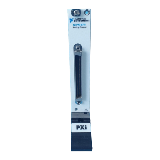
- Page 79 The following sections contain more information on the NI 6711/6713. Features (NI 6711/6713) The NI 6711/6713 are Plug-and-Play, analog output (AO), digital I/O (DIO), and timing I/O (TIO) devices for PCI bus computers. The NI 6711 features: • four AO channels with 12-bit resolution •...
- Page 80 Device-Specific Information Analog Output (NI 6711/6713) The NI 6711 has four channels of voltage output at the I/O connector, and the NI 6713 has eight channels of voltage output at the I/O connector. The reference for the AO circuitry is software-selectable per channel. The reference can be either internal or external, but the range is always bipolar.
- Page 81 Appendix A Device-Specific Information Block Diagram (NI 6711/6713) Figure A-1 shows a block diagram of the NI 6711/6713. AO 0 AO 0 AO 0 Latch 12-Bit DAC AO 1 AO 1 AO 1 Latch 12-Bit DAC AO 2 AO 2...
- Page 82 Appendix A Device-Specific Information NI DAQCard-6715 The following sections contain more information on the NI DAQCard-6715. Features (NI DAQCard-6715) The NI DAQCard-6715 is a Plug-and-Play, analog output (AO), digital I/O (DIO), and timing I/O (TIO) device for PCMCIA bus computers. The NI DAQCard-6715 features: •...
- Page 83 Analog Input Interface Timing/Control Timing/Control PFI / Trigger Trigger DAQ-STC Counter/ RTSI Bus Timing Digital I/O Timing I/O Interface Digital I/O (8) +5 V 0.75 A Figure A-2. NI DAQCard-6715 Block Diagram © National Instruments Corporation Analog Output Series User Manual...
- Page 84 Appendix A Device-Specific Information NI 6722/6723 The following sections contain more information on the NI 6722/6723. Features (NI 6722/6723) The NI 6722/6723 are Plug-and-Play, analog output (AO), digital I/O (DIO), and timing I/O (TIO) devices for PCI bus computers. The NI 6722 features: •...
- Page 85 Trigger PFI/Trigger DMA/IRQ Timing/Control DMA/IRQ DAQ - STC Timing I/O Timing Interface RTSI Bus Digital I/O Digital I/O (8) Interface *NI 6723 only. RTSI Bus Figure A-3. NI 6722/6723 Block Diagram © National Instruments Corporation Analog Output Series User Manual...
- Page 86 Appendix A Device-Specific Information NI 6731/6733 The following sections contain more information on the NI 6731/6733. Features (NI 6731/6733) The NI 6731/6733 are Plug-and-Play, analog output (AO), digital I/O (DIO), and timing I/O (TIO) devices for PCI bus computers. The NI 6731 features: •...
- Page 87 RTSI Bus Digital I/O (8) Digital I/O Timing/Control Interface +5 V RTSI Bus Note: AO 4 through AO 7 appear only on the NI 6733. Figure A-4. NI 6731/6733 Block Diagram © National Instruments Corporation Analog Output Series User Manual...
-
Page 88: Troubleshooting
Troubleshooting This section contains some common questions about AO Series devices. If your questions are not answered here, refer to the National Instruments KnowledgeBase at . It contains thousands of documents that ni.com/kb answer frequently asked questions about NI products. - Page 89 Appendix B Troubleshooting In this case, f equals 1.99 kHz, according to the following equation: 99.50 kHz 1.99 kHz ------------------------ - The smallest frequency change that you can generate in this case is approximately 10 Hz. Power-On States of the Analog Output Lines I have some motors connected directly into the outputs of my NI 6713, and when I power on my computer they start running very slowly.
- Page 90 Technical Support and Professional Services Visit the following sections of the National Instruments Web site at for technical support and professional services: ni.com • Support—Online technical support resources at ni.com/support include the following: – Self-Help Resources—For answers and solutions, visit the...
- Page 91 Appendix C Technical Support and Professional Services • Calibration Certificate—If your product supports calibration, you can obtain the calibration certificate for your product at ni.com/calibration If you searched and could not find the answers you need, contact ni.com your local office or NI corporate headquarters. Phone numbers for our worldwide offices are listed at the front of this manual.
- Page 92 Analog-to-digital converter—an electronic device, often an integrated circuit, that converts an analog voltage to a digital number. 1. Analog input 2. Analog input channel signal. AI HOLD COMP Analog input hold complete signal. © National Instruments Corporation Analog Output Series User Manual...
- Page 93 Glossary Analog output. AO 0 Analog channel 0 output signal. AO 1 Analog channel 1 output signal. AO GND Analog output ground signal. ASIC Application-Specific Integrated Circuit—a proprietary semiconductor component designed and manufactured to perform a set of specific functions. bipolar A signal range that includes both positive and negative values (for example, –5 to +5 V)
- Page 94 1. An instrument or controller you can access as a single entity that controls or monitors real-world I/O points. A device often is connected to a host computer through some type of communication network. 2. See also DAQ device and measurement device. Digital input/output. © National Instruments Corporation Analog Output Series User Manual...
- Page 95 Glossary Direct memory access—a method by which data can be transferred to/from computer memory from/to a device or memory on the bus while the processor does something else. DMA is the fastest method of transferring data to/from computer memory. Differential nonlinearity—a measure in least significant bit of the worst-case deviation of code widths from their ideal value of 1 LSB.
- Page 96 VIs and functions you can call from an application development environment (ADE), such as LabVIEW, to program all the features of an NI measurement device, such as configuring, acquiring and generating data from, and sending data to the device. © National Instruments Corporation Analog Output Series User Manual...
- Page 97 Glossary NI-DAQmx The latest NI-DAQ driver with new VIs, functions, and development tools for controlling measurement devices. The advantages of NI-DAQmx over earlier versions of NI-DAQ include the DAQ Assistant for configuring channels and measurement tasks for your device for use in LabVIEW, LabWindows/CVI, and Measurement Studio;...
- Page 98 Also called a grounded measurement system. RTSI Real-Time System Integration—the National Instruments timing bus that connects DAQ devices directly, by means of connectors on top of the devices, for precise synchronization of functions.
- Page 99 Glossary task NI-DAQmx—a collection of one or more channels, timing, and triggering and other properties that apply to the task itself. Conceptually, a task represents a measurement or generation you want to perform. terminal count The highest value of a counter. Gate hold time.
- Page 100 2. A LabVIEW software module (VI), which consists of a front panel user interface and a block diagram program. Volts, input high. Volts, input low. Volts in. Volts, output high. Volts, output low. Volts, root mean square. virtual channel See channel. © National Instruments Corporation Analog Output Series User Manual...
- Page 101 3-6 Counter 0 Gate, 5-4 minimizing glitches, 3-3 Counter 0 Internal Output, 5-5 NI 6711/6713, A-2 Counter 0 Source, 5-3 NI 6722/6723, A-6 Counter 0 Up/Down, 5-6 NI 6731/6733, A-8 Counter 1 Gate, 5-7...
- Page 102 I/O connector block diagram, A-7 68-68-pin extended AO, 2-5 features, A-6 68-pin AO, 2-1 NI 6731/6733 NI 6711 (figure), 2-2 analog output, A-8 NI 6713 (figure), 2-3 block diagram, A-9 NI 6722 (figure), 2-4 features, A-8 NI 6723 (figure), 2-5...
- Page 103 7-3 68-68-pin extended AO, 2-5 counter, 5-2 68-pin AO, 2-1 power-on state, 4-5 NI 6711 (figure), 2-2 routing, 7-1 NI 6713 (figure), 2-3 waveform generation, 3-6 NI 6722 (figure), 2-4 training, xiv NI 6723 (68-68-pin extended I/O), 2-5...