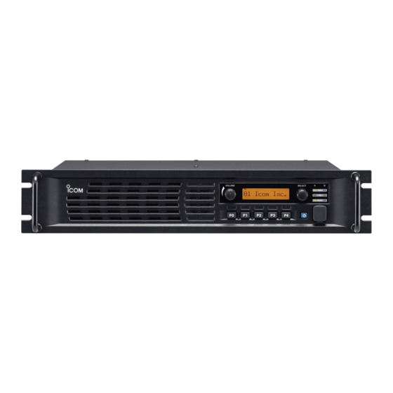
Icom IC-FR6100 Service Manual
Uhf fm repeater
Hide thumbs
Also See for IC-FR6100:
- Instruction manual (16 pages) ,
- Service manual addendum (341 pages) ,
- Instruction manual (17 pages)
Table of Contents
Advertisement
Advertisement
Table of Contents

Related Manuals for Icom IC-FR6100


Summary of Contents for Icom IC-FR6100
- Page 1 UHF FM REPEATER S-14419XZ-C1 Feb. 2008...
- Page 2 8. READ the instructions of test equipment throughly before connecting a test equipment to the repeater. Icom, Icom Inc. and logo are registered trademarks of Icom Incorporated (Japan) in the United States, the United Kingdom, Germany, France, Spain, Russia and/or other countries.
-
Page 3: Table Of Contents
CONTENTS SECTION SPECIFICATIONS SECTION INSIDE VIEWS SECTION DISASSEMBLY INSTRUCTION SECTION OPTIONAL UNIT INSTALLATION SECTION CIRCUIT DESCRIPITON RECEIVER CIRCUITS............5-1 TRANSMITTER CIRCUITS . -
Page 4: Specifications
SECTION 1 SPECIFICATIONS GENERAL [FR6000] [FR6100] • Frequency coverage 400–470 MHz [USA-01], [EXP-01] 400–470 MHz 450–520 MHz [USA-02], [EXP-02] • Conventional channels max. 32 ch • Type of emission Wide 16K0F3E/11K0F3E/11K0F7E/ 1K0F7D/ Wide 16K0F3E 11K0F7W – Middle 14K0F3E Narrow 8K50F3E/8K10F1E/8K10F1D Narrow 8K50F3E Digital 4K00F1E/4K00F1D/4K00F3E/6K00F3E... - Page 5 RECEIVER [FR6000] [FR6100] • Receive system Double-conversion superheterodyne system • Intermediate frequencies 1st IF: 46.35 MHz, 2nd IF: 450 kHz • Sensitivity Wide/Narrow Wide/Middle/Narrow 0.25 μV typ. at 12 dB SINAD –10 dBμ max. at 12 dB SINAD Digital Digital 0.25 μV typ.
-
Page 6: Section 2 Inside Views
SECTION 2 INSIDE VIEWS 1st mixer (DBM) (D62, L27, 32) Discriminator IF IC • MAIN UNIT (IC5) (X3) (TOP VIEW) RX VCOs PLL IC (RX loop) TX power AMP (IC4) (IC22) 2nd IF filter (Wide) (FI1) 2nd IF filter (Narrow) (FI2) FUNCTION Ref. - Page 7 • FRONT UNIT AF POWER AMP. (IC509) SPEAKER SW (Q508) ANALOG SW (IC506) LCD DRIVER (IC500) FRONT CPU (IC503) CLOCK OSC (X501) 2 - 2...
-
Page 8: Section 3 Disassembly Instruction
SECTION 3 DISASSEMBLY INSTRUCTION 1. Removing the front panel q Unscrew 11 screws from the top cover. w Unscrew 7 screws from the front panel. e Disconnect the cable from the MAIN UNIT assembly, and remove the front panel. 2. Removing the MAIN UNIT assembly q Uscrew 5 screws which settles the MAIN UNIT assembly. - Page 9 w Unsolder 2 points at the ANT cases. e Unscrew 4 screws from the ANT cases, Unsolder and remove them. ANT case r Disconnect the flat cabe from J4 and the speaker cable from J9. Unscrew ANT case Flat cable Disconnect t Unsolder 2 points at the bottom of ANT connectors.
-
Page 10: Section 4 Optional Unit Installation
SECTION 4 OPTIONAL UNIT INSTALLATION Install UT-109R or UT-110R as follows. q Disassembly the repeater until the MAIN UNIT is exposed. (See the page 3-1) w Modify the patterns on the MAIN UNIT as below. <MAIN UNIT (bottom side)> A and F; Cut the pattern B;... -
Page 11: Receiver Circuits
SECTION 5 CIRCUIT DESCRIPTION 5-1 TRANSMITTER CIRCUITS 5-2 RECEIVER CIRCUITS TX PLL CIRCUIT RX PLL CIRCUIT TX PLL IC (IC3) outputs resulting signal of phase- The RX PLL IC (IC4) outputs resulting signal of phase- comparison of REF signal (15.3 MHz) and feedback OSC comparison of REF signal from the TCXO (X2: 15.3 MHz) signal from TX VCO. -
Page 12: Other Circuits
IF FILTER/IF AMP CIRCUITS 5-3 OTHER CIRCUITS The 1st IF signal from the 1st mixer (L27, 32, D62) is POWER SUPPLY amplified by the post AMP (Q63, 64) and 1st stage of IF The power supply is switched by Q57 (ON/OFF). 5V (REF5) AMP (Q7) then fi... -
Page 13: Cpu (M: Ic20) Port Allocation
5-4 CPU (M: IC20) PORT ALLOCATION LINE NAME DESCRIPTION CONDITION 140–144 D0–D4 DSP data bus line. – 1–11 D5–D15 DSP data bus line. – 15–28 A1–A14 DSP data bus line. – DSP data line. – FANS Cooling fan (CH: MF1) rotation detect. "H"=While the cooling fan is rotating. - Page 14 3-4 CPU (M: IC20) PORT ALLOCATION (continued) LINE NAME DESCRIPTION CONDITION DAST Strobe to the DAC (M: IC2). – FMDA Data from the FRONT CPU (F: IC502). – MFDA Data to the FRONT CPU (F: IC502). – OPT2 Port for optional unit. –...
-
Page 15: Preparation
SECTION 6 ADJUSTMENT PROCEDURE 6-1 PREPARATION ¤ REQUIRED EQUIPMENTS EQUIPMENT SPECIFICATION EQUIPMENT SPECIFICATION Adjustment Modifi ed OPC-1122U (USB type) "CS-FR5000" (Revision 1.0 or later) JIG cable Software (see the illust below) Output voltage : 13.6 V DC [FR6000] Power attenuation : 40 dB 13.2 V DC [FR6100] Capacity : More than 60 W... - Page 16 ¤ CONNECTION <Front view> to the [MICROPHONE CONNECTOR] JIG CABLE <Rear view> OSCILLOSCOPE MODULATION ANALYZER (DC to 10 kHz) (0.1–600 MHz) ATTENUATOR (30 dB/60 W) STANDARD SIGNAL GENERATOR 20 A (0.1–600 MHz) fuses (Detect output) FREQUENCY COUNTER (0.1–600 MHz) RF POWER METER (Loose Coupling) DC power supply Black...
- Page 17 ¤ ADJUSTMENT CHANNEL LISTS Clone the adjust channels into the repeater before starting adjustment. Each channel must be assigned [Frequency], [RF PWR], [CH Type], [TX C. Tone] and [W/N] as below. • Channel list for [Low band] version • Channel list for [High band] version 6 - 3...
- Page 18 ¤ WHOLE PROCEDURE OF THE ADJUSTMENT q Connect the repeater and PC with the JIG cable (see the page 6-2). w Turn the repeater power ON. e Boot up 'CS-FR5000.' r Set the [Digital Function] to "Enable." r Click or [Read <– TR] in the [Adjust] menu, then the "Adjust Utility" window (see the page 6-5) appears. t Set or modify adjustment values as specifi...
- Page 19 ¤ ADJUST UTILITY WINDOW Mode setting TX output power Analog deviation CTCSS/DTCS deviation Squelch TX frequency Lock volatge (Preset) Lock volatge (Adjustment) S-meter Modulation balance Modulation balance (High) Digital deviation Receive sensitivity (Band center) Receive sensitivity preset Receive sensitivity (Band center) Receive sensitivity (Band high) [Low band] only [High band] only...
-
Page 20: Frequency Adjustment
6-2 FREQUENCY ADJUSTMENT 1) Select an adjustment item using cursor or [↑] / [↓] keys of the PC’s keyboard. 2) Set or modify the adjustment value as specifi ed using [←] / [→] keys of the PC’s keyboard, then push the [ENTER] key. ADJUSTMENT ADJUSTMENT ADJUSTMENT CONDITION... -
Page 21: Transmit Adjustment
6-3 TRANSMIT ADJUSTMENT 1) Select an adjustment item using cursor or [↑] / [↓] keys of the PC’s keyboard. 2) Set or modify the adjustment value as specifi ed using [←] / [→] keys of the PC’s keyboard, then push the [ENTER] key. ADJUSTMENT ADJUSTMENT ADJUSTMENT CONDITION... -
Page 22: Receive Adjustment
6-3 TRANSMIT ADJUSTMENT (continued) 1) Select an adjustment item using cursor or [↑] / [↓] keys of the PC’s keyboard. 2) Set or modify the adjustment value as specifi ed using [←] / [→] keys of the PC’s keyboard, then push the [ENTER] key. ADJUSTMENT ADJUSTMENT ADJUSTMENT CONDITION... - Page 23 6-4 RECEIVE ADJUSTMENT (continued) 1) Select an adjustment item using cursor or [↑] / [↓] keys of the PC’s keyboard. 2) Set or modify the adjustment value as specifi ed using [←] / [→] keys of the PC’s keyboard, then push the [ENTER] key. ADJUSTMENT ADJUSTMENT ADJUSTMENT CONDITION...
-
Page 24: Front Unit
SECTION 7 PARTS LIST [FRONT UNIT] [FRONT UNIT] ORDER ORDER DESCRIPTION DESCRIPTION LOCATION LOCATION IC500 1130009121 S.IC S1D15206F00A200 69.4/35.9 R571 7030005070 S.RES ERJ2GEJ 683 X (68 k) 45.8/51.5 IC501 1110005771 S.IC S-80942CNMC-G9CT2G 105.3/24 R572 7030005090 S.RES ERJ2GEJ 104 X (100 k) 46.2/50.3 IC502 1140014250 S.IC... - Page 25 [FRONT UNIT] [MAIN UNIT] ORDER ORDER DESCRIPTION DESCRIPTION LOCATION LOCATION SP501 2510001221 SP C052SB500-14 1110005330 S.IC NJM12904V-TE1 58.1/71.4 1110007290 S.IC AK2330P-L 58.7/56.1 1130010100 S.IC LMX2352TMX/NOPB 120.2/43.9 W501 8900011800 CBL OPC-1199 1130010100 S.IC LMX2352TMX/NOPB 28/78.8 W502 8900017540 CBL OPC-1785 1110003491 S.IC TA31136FNG (D,EL) 70.4/82.5 1110007280 S.IC...
- Page 26 [MAIN UNIT] [MAIN UNIT] ORDER ORDER DESCRIPTION DESCRIPTION LOCATION LOCATION 1750001070 S.DIO DAN235ETL 57.3/78.6 6200002861 S.COL NLV25T-4R7J 91.1/19.9 1750001070 S.DIO DAN235ETL 50/79.7 6130002961 S.COL #617DB-1327=P3 68.3/128.7 1790001621 S.DIO 1SV308 (TPL3,F) 70.3/93.4 6200005671 S.COL ELJRE 12NGFA 47.3/107.1 1790001621 S.DIO 1SV308 (TPL3,F) 67.8/93.4 6200005711 S.COL ELJRE 27NGFA 61.1/117.5...
- Page 27 [MAIN UNIT] [MAIN UNIT] ORDER ORDER DESCRIPTION DESCRIPTION LOCATION LOCATION 7030007290 S.RES ERJ2GEJ 222 X (2.2 k) 36.9/105.6 R198 7030007260 S.RES ERJ2GEJ 330 X (33) 103.7/62 7030005090 S.RES ERJ2GEJ 104 X (100 k) 73.7/81.1 R199 7030005050 S.RES ERJ2GEJ 103 X (10 k) 67.6/57.5 7030005530 S.RES ERJ2GEJ 100 X (10) 39/71.1...
- Page 28 [MAIN UNIT] [MAIN UNIT] ORDER ORDER DESCRIPTION DESCRIPTION LOCATION LOCATION R333 7030007350 S.RES ERJ2GEJ 393 X (39 k) B 139.3/131.4 R506 7030005110 S.RES ERJ2GEJ 224 X (220 k) 113.4/19.3 R334 7030005651 S.RES ERA3YKD 304V (300 k) 57.8/30.5 R507 7030005090 S.RES ERJ2GEJ 104 X (100 k) 115/19.3 R335 7030005871 S.RES ERA3YKD 104V (100 k)
- Page 29 [MAIN UNIT] [MAIN UNIT] ORDER ORDER DESCRIPTION DESCRIPTION LOCATION LOCATION 4030018910 S.CER C1608 JB 0J 475K-T 49.2/48.9 C191 4030017590 S.CER ECJ0EC1H070C 89.4/65.7 4030016930 S.CER ECJ0EB1A104K 57.4/50.6 C192 4030017640 S.CER ECJ0EC1H150J 90.5/56.3 4030017460 S.CER ECJ0EB1E102K 35.1/107.3 C193 4030017460 S.CER ECJ0EB1E102K 61.4/107.1 4030017460 S.CER ECJ0EB1E102K 39.9/72.7 C194...
- Page 30 [MAIN UNIT] [MAIN UNIT] ORDER ORDER DESCRIPTION DESCRIPTION LOCATION LOCATION C303 4030017370 S.CER ECJ0EC1H3R5B 131.4/82.3 C416 4550006250 S.TAN TEESVA 1A 106M8R 107.8/81.5 C304 4030017420 S.CER ECJ0EC1H470J 136.2/81.9 C417 4030016930 S.CER ECJ0EB1A104K 15/125.7 C305 4030017420 S.CER ECJ0EC1H470J 46.4/133.8 C418 4550007650 S.TAN F931V105MAABMA 39.4/73.9 C306...
- Page 31 [MAIN UNIT] [CONNECT UNIT] ORDER ORDER DESCRIPTION DESCRIPTION LOCATION LOCATION C545 4030011060 S.CER GRM31M2C2H4R0CY21L 97.6/106.8 C601 4030017420 S.CER ECJ0EC1H470J 13.8/12.4 C546 4030018910 S.CER C1608 JB 0J 475K-T 40.4/56.7 C602 4030017400 S.CER ECJ0EC1H220J 12.2/12.4 C547 4030017760 S.CER ECJ0EB1H222K 53.7/72.1 C603 4030017420 S.CER ECJ0EC1H470J 16.5/12.4 C548 4030016930 S.CER ECJ0EB1A104K...
- Page 32 SECTION 8 MECHANICAL PARTS [CHASSIS PARTS] [MAIN UNIT] ORDER ORDER DESCRIPTION QTY. DESCRIPTION QTY. 6510025220 AXK540145J 8810003361 SETSCREW (C) 3X6 ZC3 6510023091 20FLT-SM2-TB (LF) (SN) 8810003361 SETSCREW (C) 3X6 ZC3 6510023511 28FLT-SM2-TB (LF) (SN) 8110009330 3063 U-COVER 6510023110 3008L-8P8C 8110009340 3063 BOTTOM COVER 6450000140 HSJ0807-01-010 8930073980 3063 ANGLE 6510023091 20FLT-SM2-TB (LF) (SN)
- Page 33 For handles attachment MP1(C)x4 MP7(F)x11 MP2(C) KEY SEAL MP6(C) MP10(C)x2 W502(F) MP5(C)x2 MP3(C) MP4(C) MP531(F)x4 MP515(F) FRONTUNIT MP508(F) SP501(F) MP529(F)x6 MP510(F) MP533(F)x5 MP512(F) MP507(F) MP9(C)x7 S506(F) MP532(F)x6 MP519(F) W501(F) EP503(F) J503(F) EP504(F)x4 DS512(F) MP502(F) DS504(F) DS511(F) MP516(F) DS502(F) DS501(F) EP501(F) DS503(F) DS500(F) MP501(F)
-
Page 34: Main Unit (1/3)
MP24(M)x8 MP9(M) MP26(M)x4 MP14(M) MP17(M) MF1(M) MP22(M) MP23(M) MP31(M)x3 J602(CN) MP30(M)x2 MP5(C) MP11(M) MP18(M) MP32(M) W601(CN) MP19(M) MP8(M) MP16(M) J11(M) MP3(M) J10(M) MP32(M) MAIN UNIT MP29(M) MP1(M) MP6(M) MP7(M) MP15(M) MP22(M) MP21(M) W601(CN) MP5(C) MP12(M) W4(M) MP5(M) MP35(M) MP28(M) MP27(M)x19 MP37(M) MP13(M) MP10(M) -
Page 35: Main Unit (2/3)
SECTION 9 BOARD LAYOUTS • CONNECT UNIT • FRONT UNIT (TOP VIEW) (TOP VIEW) • MAIN UNIT (TOP VIEW) TX ANT DATAIN MODIN DISC AFOUT EXDA C617 EXAD DS510 EP10 DS509 EP10 DS508 DATAIN EXIO9 EXAD EXIO8 EXIO7 EXDA EXAFO DISC EXIO6 EXMOD... -
Page 36: Main Unit (3/3)
• FRONT UNIT (TOP VIEW) • CONNECT UNIT (TOP VIEW) • MAIN UNIT (TOP VIEW) J504 R542 R539 IC22 J501 R533 C532 R534 DATAIN R554 R532 C537 MODIN C527 DISC Q508 AFOUT IC506 EXDA C565 EXAD C523 C533 R572 IC503 J502 C534 EP10... - Page 37 SECTION 10 BLOCK DIAGRAM J4:28FLT-SM2-TB CONNECT UNIT EXAD EXIO1-9 EXDA D13,D14 TX VCOs HVC350B XCTS TLVIN 2SK880 #01,#03:RA55H4047M #01,#03,#22:400-470M IC26 XRTS TLVA #11,#13:RA55H4452M D 34:MA2S077 #11,#13:450-520M LV ADJ BUFF DATAIN MAX3232EIPWR XRXD #22:RA30H4047M D38:L709CE D48,D49:MA728 TXVCO1 2SC3357 EXAD XTXD 2SC5107 2SC5107 2SC5107 D44:L407CD...
- Page 38 SECTION 11 VOLTAGE DIAGRAM FRONT UNIT B2B-ZR-SM4-TF 2SB1132 EMPG3338S J504 Q508 R506 2.2K DS501 Q513 Q511 D TA114TU DTC114TU EMVR3338S R507 3.3K R558 POSW CP15S DS502 DTA114TU EMPG3338S R539 Q514 I C509 R508 2.2K R566 CP507 4.7K VCC1 GND1 Q517 R542 CP15S DS503...
- Page 39 POWER SUPPLY 3.3VA MAIN UNIT (1/3) 3.3VA *C364 R328 DSP5V DSP5V TX REFERENCE OSCILLATOR(15.3 MHz) C407 REF5 REF5 AS080340 1.5P AS080340 AS080340 *C324 *C327 *D44 C389 PLL IC AS100340 0.001 AS080340 TPLST TPLST C578 PLSSO PLSSO C310 0.001 R327 PLSCK PLSCK 2SC3357 TUNLK...
- Page 40 2SC4116 RVCO8V R102 MAIN UNIT (2/3) POWER SUPPLY RXLV R105 3.3VA 3.3VA 2SK880 RLVIN ACZ1005Y 1.2K 3.3VA 1.8U PLL IC 0.47 SVA RPLST 2SC4226 RX PLL RPLST 0.68 MSVAC103 C113 R121 *C168 *C184 R160 PLSSO PLSSO 1.2U PLSCK PLSCK OUT1 CUTO *C169 VCCIF...
-
Page 41: Connect Unit
R342 R353 NJM12902V NJM12902V ER SUPPLY MAIN UNIT (3/3) R535 IC34 R474 C513 100K C454 To D-SUB25 C586 3.3VA IC34 DATAIN C582 100P 470P 10 MSVA IC40 C581 R534 IC40 R536 C585 IC40 C588 NJM12904V C452 CONNECT UNIT VREF IC34 NJM12904V NJM12904V C441... - Page 42 • ACCESSORY CONNECTOR (CONNECT UNIT) INFORMATION CONNECT UNIT D-SUB25 pins C616 D A TAIN IO 9 EXAD IO 8 IO 7 EXDA AFOUT DISC IO 6 MODI IO 5 IO 4 IO 3 IO 2 IO 1 Pin No. Pin Name Description Specification No connection...
- Page 43 Phone : +34 (93) 590 26 70 Fax : +34 (93) 589 04 46 Glenwood Centre #150-6165 : http://www.icomspain.com Highway 17 Delta, B.C., V4K 5B8, Canada E-mail : icom@icomspain.com Phone : +1 (604) 952-4266 Fax : +1 (604) 952-0090 : http://www.icomcanada.com E-mail : info@icomcanada.com Unit 9, Sea St., Herne Bay, Kent, CT6 8LD, U.K.
- Page 44 S-14419XZ-C1 1-1-32, Kamiminami, Hirano-ku, Osaka 547-0003, Japan © 2008 Icom Inc.