Table of Contents
Advertisement
Quick Links
QQ
3 7 63 1515 0
TE
L 13942296513
www
.
http://www.xiaoyu163.com
SERVICE MANUAL
SERVICE MANUAL
DVD PLAYER
MODEL
Black, Silver and Golden models
B MDD, B MDC
B MUT, B MUS, B MUP
G MUT, G MUS, G MUR, G MUK
S MUP
SAFETY-RELATED COMPONENT
WARNING!!
THE MARK
PARTS INDICATES THE CRITICAL FOR RISK OF
FIRE AND ELECTRIC SHOCK.
WHEN REPLACING, BE SURE TO USE PARTS OF
IDENTICAL DESIGNATION.
MAKE LEAKAGE-CURRENT OR RESISTANCE
MEASUREMENTS TO DETERMINE THAT EXPOSED
PARTS ARE ACCEPTABLY INSULATED FROM THE
SUPPLY CIRCUIT BEFORE RETURNING THE
APPLIANCE TO THE CUSTOMER.
x
ao
u163
y
i
http://www.xiaoyu163.com
2 9
8
DV-SP500
Q Q
3
6 7
1 3
1 5
120V AC, 60Hz
110 - 240V AC, 50/60Hz
FOUND ON SOME COMPONENT
co
.
9 4
2 8
Ref. No. 3724
072002
ON
OPEN/CLOSE
ON
TV
TV
ON/STANDBY
ON /ST ANDB Y
STANDBY
STANDBY
ANGLE
AUDIO
SUBTITLE
LAST M
COND. M
DIMMER
DISPLAY
LAST M
TOP MENU
MENU
TOP MENU
CH -
CH +
CH-
VOL +
ENTER
VOL -
RETURN
SETUP
RETURN
TV/ VCR
TV/ VCR
PAUSE
STOP
PAUSE
PLAY
FR
FF
DOWN
UP
FR
STEP/SLOW
+
1
2
3
1
-
4
5
6
4
FUNCTION M
7
8
9
7
SEARCH
CLEAR
+10
0
+10
RANDOM REPEAT
A-B
PROGRAM
RANDOM REPEAT
REMOTE CONTROLLER RC- 449 DV
REMOTE CONTROLLER RC- 450 DV
DVD
TV
DVD
DVD
RC-449DV
RC-450DV
U.S.A., Canadian
Other models
models only
0 5
8
2 9
9 4
2 8
m
DV-SP500
9 9
OPEN/CLOSE
ANGLE
AUDIO
SUBTITLE
COND. M
DIMMER
DISPLAY
MENU
CH+
VOL +
ENTER
VOL -
SETUP
STOP
PLAY
FF
DOWN
UP
STEP/SLOW
+
2
3
-
5
6
FUNCTION M
8
9
SEARCH
CLEAR
0
A-B
PROGRAM
TV
TV
9 9
Advertisement
Table of Contents

Related Manuals for Onkyo DV-SP500


Summary of Contents for Onkyo DV-SP500
-
Page 1: Dvd Player
DV-SP500 3 7 63 1515 0 Ref. No. 3724 072002 SERVICE MANUAL SERVICE MANUAL DVD PLAYER DV-SP500 MODEL OPEN/CLOSE OPEN/CLOSE ON/STANDBY ON /ST ANDB Y STANDBY STANDBY ANGLE AUDIO SUBTITLE ANGLE AUDIO SUBTITLE LAST M COND. M DIMMER DISPLAY LAST M COND. -
Page 2: Specifications
DV-SP500 3 7 63 1515 0 SPECIFICATIONS General Power supply AC 100 – 240 V, 50/60 Hz Power consumption 15 W Power consumption (standby mode) 2.6 W Weight 3.4 kg External dimensions 312 mm (W/H/D) Signal system PAL/Auto mode Regional restriction code U.S.A. -
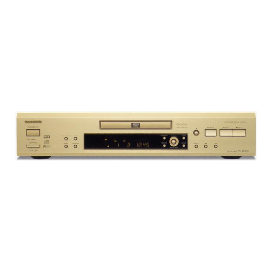
Page 3: Front Panel
When STANDBY/ON button is pressed to ON while the POWER PAUSE button switch is set to ON, the DV-SP500 turns on and the STANDBY Press during playback to pause. Press again to resume playback. indicator turns off. Pressing the button again returns the DV- STOP button SP500 to the standby state. -
Page 4: Rear Panel
DV-SP500 3 7 63 1515 0 PANEL VIEW -2 FL DISPLAY 10 11 V CD LAST TITLE CHP TRACK TOTAL REMAIN COND D indicator REPEAT indicator Inserted disc indicator TOTAL/REMAIN indicator TITLE indicator LAST indicator GUI (Graphical User Interface) indicator... - Page 5 DV-SP500 3 7 63 1515 0 PANEL VIEW - 3 REMOTE CONRTOLLER FR/FF buttons During playback of DVD and Video CD, press to perform fast forward scanning or to perform fast reverse scanning of DVD OPEN / CLOSE and Video CD. When a CD or MP3 is loaded, audio scanning is STANDBY performed.
- Page 6 DV-SP500 3 7 63 1515 0 SERVICE PROCEDURES-1 1. Replacing the fuses 2. Safety-check out (Only U.S.A. model) This symbol located near the fuse indicates that the After correcting the original service problem perform the fuse used is show operating type, For continued protection against...
- Page 7 DV-SP500 3 7 63 1515 0 SERVICE PROCEDURES-2 4. Remove the solder of Laser Diode shorting Connect Pickup and DVD main circuit PC board by FFC(3 pcs). Fix it with the DVD Mechanism Remove the solder of Laser Diode shorting on Pickup.
-
Page 8: Trouble Shooting
DV-SP500 3 7 63 1515 0 TROUBLE SHOOTING No Power ON FL is not turned ON FL indication is unusual START Power ON Blow out fuse of the primary side Blow out micro-fuse on the POWER SUPPLY Unit. (Check the each voltage.) (P901(Output PCB) and CN2(Power supply unit)) FL controller IC (Q701) on the Display PCB Assy is damaged. -
Page 9: Error Message
DV-SP500 3 7 63 1515 0 ERROR MESSAGE ERROR CODE Error codes that are displayed on the FL display without using the remote control unit FL Display Possible causes Operation of the unit The sound may not out AV1 VER AV-1 chip is not a match with the program of system controller with the specific audio. - Page 10 DV-SP500 3 7 63 1515 0 ADJUSTMENT PROCEDURE-1 ADJUSTMENT ITEMS AND JIGS AND MEASURING LOCATION INSTRUMENTS Adjustment Items [Mechanism Part] Tangential and Radial Height Coarse Adjustment DVD Jitter Adjustment Initialize the Focus Sweep Setting [Electrical Part] Screwdriver (large) Screwdriver (medium) Electrical adjustments are not required.
-
Page 11: Mechanism Adjustment
DV-SP500 3 7 63 1515 0 ADJUSTMENT PROCEDURE-2 MECHANISM ADJUSTMENT Tangential and Radial Height Coarse Adjustment START Cautions: Remove the servo mechanism. Because there is not a Spacer for height adjustment in Remove a Spacer for height adjustment adjustment after the second time, will keep it at need. - Page 12 DV-SP500 3 7 63 1515 0 ADJUSTMENT PROCEDURE-3 NECESSARY ADJUSTMENT POINTS Adjustment Points When Exchange Parts of Mechanism Assy Mechanical After adjustment, screw locks Exchange the Pickup 1, 2, 3 point with the Screw tight. Electric point Mechanical Exchange the Traverse Mechanism...
- Page 13 DV-SP500 3 7 63 1515 0 UPGRADE OF FIRMWARE-1 Preparation Remote controller Part No. 24140451S Same as DV-S757 or DV-S555 Interface jig Part No. 0J13 Part No. GGF1348 RS-232C Cable (Straight type) When used 0J13 L 13942296513 When used GGF1348...
- Page 14 NOTE: This is one example. 1. ok_down.exe C:dvsp500fw Rewriting tools 2. down.bat Rewriting tools 3. b1ck1048.sz0 Firmware program The file name changes with versions of the firmware. When new FW program is required, Please ask to ONKYO Technical Information Group. dvsp500fw u163 http://www.xiaoyu163.com...
- Page 15 DV-SP500 3 7 63 1515 0 UPGRADE FIRMWARE-3 Download procedures [NOTES] This procedure's picture is using Japanese PC. The program file name and the folder name etc. are examples. 1. Start, MS-DOS prompt using the start-up menu of PC.
- Page 16 DV-SP500 3 7 63 1515 0 UPGRADE FIRMWARE-4 7. Setting the Region code. When display the TV monitor is "RIGIN INI", key input the rigoinal code by remote controller. * MDD1N and MJJ2N are automatically chosen. (Automatically witting) Destination...
- Page 17 DV-SP500 3 7 63 1515 0 Disassembly of the Traverse Mechanism Assy-1 Remove the top cover and Tray Panel. Remove the Loading Mechanism Assy (Screws 4). Remove the Tray panel and Front Panel. Remove a screw. Remove the Bridge (Screw 1).
- Page 18 DV-SP500 3 7 63 1515 0 Disassembly of the Traverse Mechanism Assy-2 When Removing The Pickup Assy Remove two screws. Remove the Pickup Flexible Cable. Cautions: Screw is locked with Screw Lock. Please lock it with Screw Lock when installs it.
- Page 19 DV-SP500 3 7 63 1515 0 Disassembly of the Traverse Mechanism Assy-3 Styling the Pickup Flexible Cable Fold a edge of lining part of the Pickup Flexible Cable. Insert the Pickup Flexible Cable in connector, and lock it surely.
- Page 20 DV-SP500 3 7 63 1515 0 EXPLODED VIEW (LOADING MECHANISM) / PARTS LIST EXPLODED VIEW (LOADING MECHANISM) / PARTS LIST Z101 : DVD Mechanism DB-VLD301 GEM1036 GEM1036 To DVDM CN151 Lubricating Oil GYA1001 L 13942296513 Lubricating Oil Lubricating Oil...
- Page 21 DV-SP500 3 7 63 1515 0 EXPLODED VIEW / PARTS LIST TRAVERSE MECHANISM ASSY 17 (Torque : 0.12+/- 0.01 N m) 4 (Adjustment Screw) 4 (Adjustment Screw) (Torque : 0.12+/- 0.01 N m) L 13942296513 17 (Torque : 0.12+/- 0.01 N m) TRAVERSE MECHANISM ASSY-S PARTS LIST Mark No.
- Page 22 DV-SP500 3 7 6 3 1 5 1 5 0 EXPLODED VIEW E903 Z101 Z103 Z102 Z104 To DVD Z104 Mechanism To DVD Mechanism Z100 E701 L 1 3 9 4 2 2 9 6 5 1 3 E702 : Torque 1.6+/-0.5kgf...
- Page 23 DV-SP500 3 7 63 1515 0 EXPLODED VIEW PARTS LIST-1 CHASSIS SECTION REF. REF. PART NO. DESCRIPTION PART NO. DESCRIPTION 27100399B Chassis 27122992 Rear panel <B MDD/MDC> 27175316B 27122993 Rear panel <B MUT/G MUT/MUK> 28141332 Cushion 27122994 Rear panel <B MUS/G MUS>...
- Page 24 DV-SP500 3 7 63 1515 0 EXPLODED VIEW PARTS LIST-2 CHASSIS SECTION REF. REF. PART NO. DESCRIPTION PART NO. DESCRIPTION 1H492510-1A NAPS-7610-1A, AC inlet terminal 24150020A NGPS-0020-120V, Power PC board assy <MDD/MDC> supply unit <MDD/MDC> 1H492510-1B NAPS-7610-1B, AC inlet terminal...
- Page 25 DV-SP500 3 7 63 1515 0 ICs BLOCK DIAGRAM / TERMINAL DESCRIPTION Q301 : PCM1742KE (Digital/ Analog signal converter) Pin layout Terminal Description Name Pin Function Audio data bit clock input DATA Audio data digital input DATA L-channel and R-channel Audio data...
- Page 26 DV-SP500 3 7 63 1515 0 ICs BLOCK DIAGRAM / TERMINAL DESCRIPTION IC807 : PD0274A Audio Quality Enhancer (AQE) Block Diagram IBS, TFS, IFS, LRIPOL, IFORM, CKSEL, TEST IBS, BES, DIR Bit Extension LRCK Pin Arrangement DAIN Input LRCK...
- Page 27 DV-SP500 3 7 63 1515 0 ICs BLOCK DIAGRAM / TERMINAL DESCRIPTION IC601 : PD6345A FR CPU Pin Function-1 utput L 13942296513 u163 http://www.xiaoyu163.com...
- Page 28 DV-SP500 3 7 63 1515 0 ICs BLOCK DIAGRAM / TERMINAL DESCRIPTION Pin Function-2 t i s t i s d i l t i s l l o l l o " r " L L 13942296513 " : "...
- Page 29 DV-SP500 3 7 63 1515 0 ICs BLOCK DIAGRAM / TERMINAL DESCRIPTION Pin Function-3 XVQEST i t l c t i c t i " " L " ) " l a i l a i l a i...
- Page 30 DV-SP500 3 7 63 1515 0 ICs BLOCK DIAGRAM / TERMINAL DESCRIPTION Pin Function-4 x i f x i f L 13942296513 u163 http://www.xiaoyu163.com...
- Page 31 DV-SP500 3 7 63 1515 0 ICs BLOCK DIAGRAM / TERMINAL DESCRIPTION IC881 : PM0026A Progressive Converter Except <MUP> model Pin Layout VDD2 VDD3 SPR4/VO6 SDATA SPR5/VO7 SCLK SPR6/VO8 RMA1 RMA0 SPR7/VO9 CKPOL CLMP VIA9 AGND VIA8 VIA7 AVDD2...
- Page 32 DV-SP500 3 7 63 1515 0 ICs BLOCK DIAGRAM / TERMINAL DESCRIPTION Pin Function-1 L 13942296513 t s i i l p l l e l a i e l l l a i e l l u163 http://www.xiaoyu163.com...
- Page 33 DV-SP500 3 7 63 1515 0 ICs BLOCK DIAGRAM / TERMINAL DESCRIPTION Pin Function-2 Pin Function l a i e l l t s i L 13942296513 t s i y t i c i t u163 http://www.xiaoyu163.com...
- Page 34 DV-SP500 3 7 63 1515 0 ICs BLOCK DIAGRAM / TERMINAL DESCRIPTION Q601 : TC4053BF Triple 2-Channel multiplexer / demultiplexer 1Y 1 16 V 0Y 2 15 Y-COM X-COMMON 1Z 3 14 X-COM I / O O / I...
- Page 35 DV-SP500 3 7 63 1515 0 ICs BLOCK DIAGRAM / TERMINAL DESCRIPTION Q401 - Q404 : NJM4565M Opertational amplifier L 13942296513 u163 http://www.xiaoyu163.com...
- Page 36 DV-SP500 3 7 63 1515 0 ICs BLOCK DIAGRAM / TERMINAL DESCRIPTION Q602 : TC74HCT00AP 2-Input NAND gate 14 Vcc 1A 1 13 4B 1B 2 12 4A 1Y 3 Truth table 11 4Y 2A 4 10 3B 2B 5...
- Page 37 DV-SP500 3 7 63 1515 0 ICs BLOCK DIAGRAM / TERMINAL DESCRIPTION Q352 : TC74VHCU04FT Hex inverter Pin layout 14 Vcc 13 6A 12 6Y 11 5A Truth table 10 5Y 9 4A 8 4Y L 13942296513 u163 http://www.xiaoyu163.com...
- Page 38 DV-SP500 3 7 6 3 1 5 1 5 0 MICROPROCESSOR TERMINAL DESCRIPTION Q701 : uPD780232GC No. SYMBOL FUNCTION DESCRIPTION No. SYMBOL FUNCTION DESCRIPTION VDD1 VDD1 Power supply, +5V P45/FIP37 SMP192LED Sampling rate 192LED control output pin P44/FIP36 SAMP96LED...
- Page 39 DV-SP500 3 7 63 1515 0 FL TUBE VIEW Pin connection DVD-AUDIO DVD-AUDIO SACD V CD SACD V CD PBCRANDOM RANDOMMEMORY MEMORY 1A-B 1A-B LFE LAST LAST D.MIX D.MIX COND. PRO LOGIC PRO LOGIC TITLE TITLE GROUP GROUP CHP TRACK...
- Page 40 DV-SP500 3 7 63 1515 0 ICs BLOCK DIAGRAM / TERMINAL DESCRIPTION IC101 : LA9701M RF Amplifier Block Diagram PDRFÐ EQI2 REF1 Scratch Detection EFMO PDRF RREC L 13942296513 TEÐ FIN1 FIN2 LDD1 TESI LDS1 u163 http://www.xiaoyu163.com...
- Page 41 DV-SP500 3 7 63 1515 0 ICs BLOCK DIAGRAM/ TERMINAL DESCRIPTION Q207 : LA73054 (6-CHANNEL VIDEO DRIVER) Block Diagram AMP1 3 SW CC +5V (9dB/6dB) COMPOSITE IN CLAMP 2 Drive/1 Drive SQUEEZE SW 2 Step Amp 1 C_OFFSET CC +5V...
- Page 42 DV-SP500 3 7 63 1515 0 ICs BLOCK DIAGRAM / TERMINAL DESCRIPTION IC201 : LC78652W Servo DSP IC Block Diagram SLDO Servo TILTE 8bit 8bit SPDO Processor RF_PH (16 x16+32 32) TBAL RF_BH TILTDO AUXO JITT HFLIO Track Counter...
- Page 43 DV-SP500 3 7 63 1515 0 ICs BLOCK DIAGRAM / TERMINAL DESCRIPTION LC78652W-2 Pin Function t f i l l i L 13942296513 t t i y t i t l i a i l t l i u163...
- Page 44 DV-SP500 3 7 63 1515 0 ICs BLOCK DIAGRAM / TERMINAL DESCRIPTION LC78652W-3 r r i signals 53 PP0/DVD CDB PP1/CRCERRB PP2/EVENT t i r L 13942296513 l a i t f i l l i l i f...
- Page 45 DV-SP500 3 7 63 1515 0 ICs BLOCK DIAGRAM / TERMINAL DESCRIPTION IC801 : M65774BFP MPEG2 Decoder IC 16M bit SDRAM Block Diagram SDRAM Bit Streem Descrambler Controller Bit Streem Input Interface Video Decoder Sub-picture Decoder Internal Display Processor...
- Page 46 DV-SP500 3 7 63 1515 0 ICs BLOCK DIAGRAM/ TERMINAL DESCRIPTION Pin Function-2 Function n Function 84 VSYNC utput HSYNC l output put for external sync. CSYNC nal input OSDKEY ee-running clock) L 13942296513 d normally Data transfer line with DRAM...
- Page 47 DV-SP500 3 7 63 1515 0 ICs BLOCK DIAGRAM / TERMINAL DESCRIPTION Pin Function-3 / I/O Pin Name / I/O n Function Pin Name Pin Function n i l Ground NMD9 n i l NMD7 n i l NMD8...
- Page 48 DV-SP500 3 7 63 1515 0 ICs BLOCK DIAGRAM / TERMINAL DESCRIPTION IC861 : ADV7172KST Video Encoder Pin Layout 47 46 45 44 43 42 41 40 39 38 37 COMP1 DAC A DAC B DAC C DACD CSO_HSO...
- Page 49 DV-SP500 3 7 63 1515 0 ICs BLOCK DIAGRAM / TERMINAL DESCRIPTION Pin Function . s l . s l l r t 0 " . " l a i t s i - l l i l p s "...
- Page 50 DV-SP500 3 7 63 1515 0 ICs BLOCK DIAGRAM / TERMINAL DESCRIPTION IC251 : BA6664FM Three-phase Motor Driver Block Diagram A3 2 DRIVER A2 4 GAIN GAIN SWITCH CONTROL A1 7 CURRENT SENSE AMP HALL AMP TORQUE GND 8...
-
Page 51: Block Diagram
DV-SP500 3 7 6 3 1 5 1 5 0 BLOCK DIAGRAM U3 : AC INLET PC BOARD U20 : Power supply unit NGPS-0021-100V - 240V <MUT,MUS,MUR,MUK,MUP> DB-VPB307 NGPS-0020-120V <MDD,MDC> DVD Traverse Mechanism PICK UP U1 : OUTPUT TERMINAL PC BOARD... - Page 52 DV-SP500 3 7 6 3 1 5 1 5 0 PC BOARD CONNECTION DIAGRAM NAPS-7610 D Terminal Inlet terminal <MJJ> model only PC board : NAAR-7605 P982A P982B Z100 : Main circuit PC board Output terminal PC board P104...
- Page 53 http://www.xiaoyu163.com 3 7 63 1515 0 PRINTED CIRCUIT BOARD VIEW : STANDBY LED PC BOARD (NADIS-7612) S723 25137612 NCDIS-7612 Component side view L 13942296513 Q722 DPS-5.3 Soldering side view WHITE P982B : POWER SWITCH PC BOARD (NASW-7613) P981B P981B u163 25137613 S991 NCSW-7613...
- Page 54 DV-SP500 3 7 63 1515 0 : SCART TERMINAL PC BOARD (NAETC-7614) J350 NCETC-7614 J351 25137614 J352 J353 J354 Q610 Q611 Q612 C604 J367 J368 P601 E601B E601A Component side view Q602 D602 Q605 Q602 L 13942296513 Q606 Q608...
- Page 55 http://www.xiaoyu163.com 3 7 63 1515 0 SCHEMATIC DIAGRAM (Page 1) Z100 :Main circuit PC board (DB-VPB306/301) (RF) Page 2 L 13942296513 CN120 (RF) CN251 To Stepp (Carr CN151 For Mecha u163 connector http://www.xiaoyu163.com...
- Page 56 DV-SP500 3 7 63 1515 0 (RF) : RF SIGNAL ROUTE : RF (VIDEO) SIGNAL ROUTE TC7SZU04F Page 2 IC304 : RF (AUDIO) SIGNAL ROUTE (AD) : AUDIO DATA SIGNAL ROUTE Page 3 : FOCUS SERVO LOOP LINE : TRACKING SERVO LOOP LINE 3.3k...
- Page 57 http://www.xiaoyu163.com 3 7 63 1515 0 SCHEMATIC DIAGRAM (Page 2) Z100 :Main circuit PC board (DB-VPB306/301) VYW1958-A L 13942296513 R607 6.8k CN512 MECHA Page1 u163 page 1 IC201 To CN15 Page 4 http://www.xiaoyu163.com...
- Page 58 DV-SP500 3 7 63 1515 0 CLOCK GENERATOR Page 1 R489 L 13942296513 : The power supply is shown with the marked box. : AUDIO (DIGITAL) SIGNAL ROUTE CN401 u163 http://www.xiaoyu163.com...
- Page 59 http://www.xiaoyu163.com 3 7 63 1515 0 SCHEMATIC DIAGRAM (Page 3) Z100 :Main circuit PC board (DB-VPB306/301) To SCRUT 7,21, 68, 188P IC712 4M MSM51V17805D-60TS (VD) L 13942296513 Page 1 IC201 Page 1 R334 Page 2/ IC601 to Page 1 Page 3 IC 801 u163 Page 2 IC 601 Page 1 IC 201...
- Page 60 DV-SP500 3 7 63 1515 0 <MUP> model only <MUP> model only IC806 IC806 : RF (VIDEO) SIGNAL ROUTE (VD) : VIDEO DATA SIGNAL ROUTE (AD) : AUDIO DATASIGNAL ROUTE : AUDIO SIGNAL ROUTE : AUDIO (DIGITAL) SIGNAL ROUTE...
- Page 61 http://www.xiaoyu163.com 3 7 63 1515 0 SCHEMATIC DIAGRAM (Page 4) Z100 :Main circuit PC board (DB-VPB306/301) Page 3 Page 2 (VD) (VD) (Cr) (Cr) (Cr) (Cb) (Cb) (Cb) L 13942296513 Progresive converter circuit is not used European model Page 3 (Cr) (VD) (VD)
- Page 62 DV-SP500 3 7 63 1515 0 Except <MUP> model (VD) : VIDEO DATASIGNAL ROUTE : V SIGNAL ROUTE : Y SIGNAL ROUTE : C SIGNAL ROUTE : Y SIGNAL ROUTE (Cb) : Cb SIGNAL ROUTE (Cr) : Cr SIGNAL ROUTE...
- Page 63 http://www.xiaoyu163.com 3 7 63 1515 0 SCHEMATIC DIAGRAM -1 : OUTPUT TERMINAL PC BOARD S C K NAAR-7605 S C K C 3 5 4 C 3 5 5 2 3 2 S O 2 3 2 S O L 3 5 1 B K 1 6 0 8 L M 1 8 2 - T 0 2 0 0 2 0...
- Page 64 DV-SP500 3 7 63 1515 0 P291 D Terminal MJJ2N Only Q 2 6 6 NAETC-7608 <MJJ> only OPTICAL_OUT R 2 7 2 R N 2 4 0 3 Q 3 5 1 C 3 6 0 Q 2 6 5...
- Page 65 http://www.xiaoyu163.com 3 7 63 1515 0 SCHEMATIC DIAGRAM - 2 : DISPLAY CIRCUIT PC BOARD R 7 4 7 R 7 4 8 R 7 4 9 Q 7 0 5 (NADIS-7606) 3 9 0 4 7 0 8 2 0 R E M S E N S Destination R720...
- Page 66 DV-SP500 3 7 63 1515 0 T o P 9 0 2 : STANDBY LED C N 2 PC BOARD (NADIS-7612) R 7 4 9 R 7 5 0 R 7 7 1 R 7 7 2 : POWER SUPPLY UNIT 8 2 0 1 .
- Page 67 http://www.xiaoyu163.com 3 7 63 1515 0 SCHEMATIC DIAGRAM - 3 <MUP> model only : SCART TERMINAL PC BOARD NAETC-7614 V + 1 2 V Q 6 0 6 Q 6 0 5 R 6 2 4 2 S C 2 7 1 2 2 S C 2 7 1 2 6 .
- Page 68 DV-SP500 3 7 63 1515 0 Q 6 0 9 2 S D 6 5 5 R 6 2 9 R 6 3 0 Q 6 1 0 Q 6 0 8 2 S D 6 5 5 R N 1 4 0 2...
-
Page 69: Schematic Diagram
DV-SP500 3 7 6 3 1 5 1 5 0 SCHEMATIC DIAGRAM Power supply unit AC4.5V 47ohm 24150020A NGPS-0020 <MDD> 24150021A NGPS-0021 <MUP/MUT/MUS> -27V 5-15mA Except <MDD> D1-D4 SW+15V 50-400mA SW+3.3V PHC2-2 400-900mA AC-H AC-G L 1 3 9 4 2 2 9 6 5 1 3... - Page 70 DV-SP500 3 7 63 1515 0 PRINTED CIRCUIT BOARD VIEW Except <MUP> model Z100 : Main circuit PC board DB-VPB306 L 13942296513 u163 SIDE A http://www.xiaoyu163.com...
- Page 71 DV-SP500 3 7 63 1515 0 PRINTED CIRCUIT BOARD VIEW Except <MUP> model Z100 : Main circuit PC board DB-VPB306 L 13942296513 u163 SIDE B http://www.xiaoyu163.com...
- Page 72 DV-SP500 3 7 63 1515 0 PRINTED CIRCUIT BOARD VIEW <MUP> model only Z101 : MAIN CIRCUIT PC BOARD DB-VPB301 L 13942296513 Top pattern and top silk u163 http://www.xiaoyu163.com...
- Page 73 DV-SP500 3 7 63 1515 0 PRINTED CIRCUIT BOARD VIEW FROM SOLDERING SIDE-1 : OUTPUT TERMINAL PC BOARD (NAAR-7605) R129 L353 C901 C909 R357 C907 C364 R351 C351 C913 D901 D920 R902 R352 C905 Q901 Q920 R505 SW_5V L351...
- Page 74 http://www.xiaoyu163.com 3 7 63 1515 0 PRINTED CIRCUIT BOARD VIEW FROM SOLDERING SIDE : DISPLAY CIRCUIT PC BOARD (NADIS-7606) P731 Q703B J710 P701B J709 P710A PLAY STOP OPEN MENU D705 D704 D703 PAUSE S711 S710 TOP-MENU S709 S703 S701 J712 J706 DISPLAY S702...
- Page 75 DV-SP500 3 7 63 1515 0 D707 NCDIS-7606 25137606 D706 J748 J747 Q724 J746 Q723 LAST_MEMORY CLEAR J735 R785 R5761 S712 S715 Q705 J737 J736 J733 Q705 S713 S714 J734 RANDOM REPEAT J739 R5761 onent side view L 13942296513...
- Page 76 DV-SP500 3 7 63 1515 0 PRINTED CIRCUIT BOARD VIEW FROM SOLDERING SIDE-1 : OUTPUT TERMINAL PC BOARD (NAAR-7605) C915 P902 CN102 J328 CN102 J295 C910 C906 C902 J327 C908 C912 C911 C904 J280 NCAR-7605 C920 C420 J339 25137605B...
- Page 77 DV-SP500 3 7 63 1515 0 PRINTED CIRCUIT BOARD PARTS LIST-1 U1 : OUTPUT TERMINAL PC BOARD CIRCUIT NO. PART NO. DESCRIPTION (NAAR-7605-1A/1B/1C/1D/1F)) Pin jacks P201 25045656 NPJ-5PDBY456 CIRCUIT NO. PART NO. DESCRIPTION P203 25045654 NPJ-3PDGLR454 Q205 22241228R2 TC74HC4053AF Except <MUP>...
- Page 78 DV-SP500 3 7 63 1515 0 PRINTED CIRCUIT BOARD PARTS LIST-2 U2 : DISPLAY CIRCUIT PC BOARD U5 : STANDBY LED PC BOARD (NADIS-7606-1A/1B/1C/1D/1F)) (NADIS-7612-1A/1B/1C/1D/1F)) CIRCUIT NO. PART NO. DESCRIPTION CIRCUIT NO. PART NO. DESCRIPTION Transistor Q701 22241880R3 MPD780232GC-077-8BT...
- Page 79 DV-SP500 3 7 63 1515 0 PACKING VIEW P20, P21,P22 Tape P19 Except <MUP> RC-449DV <MDD/MDC> RC-450DV <MUP/MUT/ MUS/MUR> <MUP> <MUT, MUS, P981 MUR, MUK> P17 <MUP> Front side L 13942296513 u163 http://www.xiaoyu163.com...
- Page 80 DV-SP500 3 7 63 1515 0 PACKING VIEW PARTS LIST REF. REF. PART NO. DESCRIPTION PART NO. DESCRIPTION 29091986 Pad assy 2010200 RI cord, 3.5-MINI PLUG 29100037-1A Poly bag, 650 x 500 24140449 Remote controller, RC-449DV <MDD/MDC> 29110148 PP Tape...
- Page 81 Sales & Product Planning Div. : 2-1, Nisshin-cho, Neyagawa-shi, OSAKA 572-8540, JAPAN Tel: 072-831-8111 Fax: 072-833-5222 ONKYO U.S.A. CORPORATION 18 Park Way, Upper Saddle River, N.J. 07458, U.S.A. Tel: 201-785-2600 Fax: 201-785-2650 E-mail: onkyo@onkyousa.com ONKYO EUROPE ELECTRONICS GmbH Industriestrasse 20, 82110 Germering, GERMANY Tel: 089-849-320 Fax: 089-849-3265 E-mail: info@onkyo.de...