Sony CDX-M30 Service Manual
Hide thumbs
Also See for CDX-M30:
- Operating instructions manual (140 pages) ,
- Service manual (42 pages) ,
- Installation/connections (2 pages)
Table of Contents
Advertisement
SERVICE MANUAL
Ver. 1.0 2007. 08
• The tuner and CD sections have no adjustments.
AUDIO POWER SPECIFICATIONS
POWER OUTPUT AND TOTAL HARMONIC DISTORTION
23.2 watts per channel minimum continuous average power into
4 ohms, 4 channels driven from 20 Hz to 20 kHz with no more
than 5% total harmonic distortion.
CD player section
Signal-to-noise ratio
120 dB
Frequency response
10 – 20,000 Hz
Wow and flutter
Below measurable limit
Tuner section
FM
Tuning range
87.5 – 108.0 MHz (at 50 kHz step)
87.5 – 107.9 MHz (at 200 kHz step)
FM tuning interval
50 kHz/200 kHz switchable
Antenna (aerial) terminal
External antenna (aerial) connector
Intermediate frequency 10.7 MHz/450 kHz
Usable sensitivity
9 dBf
Selectivity
75 dB at 400 kHz
Signal-to-noise ratio
67 dB (stereo), 69 dB (mono)
Harmonic distortion at 1 kHz
0.5% (stereo), 0.3% (mono)
Separation
35 dB at 1 kHz
Frequency response
30 – 15,000 Hz
AM
Tuning range
531 – 1,602 kHz (at 9 kHz step)
530 – 1,710 kHz (at 10 kHz step)
AM tuning interval
9 kHz/10 kHz switchable
Antenna (aerial) terminal
External antenna (aerial) connector
Intermediate frequency 10.7 MHz/450 kHz
Sensitivity
30 µV
Sony Corporation
9-887-819-01
eVehicle Division
2007H04-1
Published by Sony Techno Create Corporation
© 2007. 08
CDX-M30
Model Name Using Similar Mechanism
CD Drive Mechanism Type
Optical Pick-up Name
SPECIFICATIONS
Power amplifier section
Outputs
Speaker impedance
Maximum power output
General
Output
Inputs
Tone controls
FM/AM COMPACT DISC PLAYER
US Model
CDX-GT52W/GT520
MG-101FC-188//Q
DAX-25A
Speaker outputs (sure seal connectors)
4 – 8 ohms
52 W × 4 (at 4 ohms)
Audio outputs terminal (front, rear/sub
switchable)
Power antenna (aerial) relay control terminal
Power amplifier control terminal
Telephone ATT control terminal
Illumination control terminal
BUS control input terminal
BUS audio input terminal
Remote controller input terminal
Antenna (aerial) input terminal
AUX input jack (stereo mini jack)
Low: ±10 dB at 60 Hz (XPLOD)
Mid: ±10 dB at 1 kHz (XPLOD)
High: ±10 dB at 10 kHz (XPLOD)
– Continued on next page –
Advertisement
Table of Contents

Related Manuals for Sony CDX-M30


Summary of Contents for Sony CDX-M30
- Page 1 AM tuning interval 9 kHz/10 kHz switchable Antenna (aerial) terminal External antenna (aerial) connector Intermediate frequency 10.7 MHz/450 kHz Sensitivity 30 µV FM/AM COMPACT DISC PLAYER Sony Corporation 9-887-819-01 eVehicle Division 2007H04-1 Published by Sony Techno Create Corporation © 2007. 08...
- Page 2 COMPONENTS IDENTIFIED BY MARK 0 OR DOTTED LINE WITH MARK 0 ON THE SCHEMATIC DIAGRAMS AND IN THE PARTS LIST ARE CRITICAL TO SAFE OPERATION. REPLACE THESE COMPONENTS WITH SONY PARTS WHOSE PART NUMBERS APPEAR AS SHOWN IN THIS MANUAL OR IN SUPPLEMENTS PUBLISHED BY SONY.
-
Page 3: Table Of Contents
CDX-M30 • CD Playback TABLE OF CONTENTS You can play CD-DA (also containing CD TEXT) and CD-R/ CD-RW (MP3/WMA/AAC files). SERVICE NOTE ............4 Type of discs Label on the disc GENERAL Location of controls and basic operations ....... 5 Connections .............. -
Page 4: Service Note
CDX-M30 SECTION 1 SERVICE NOTE EXTENSION CABLE AND SERVICE POSITION When repairing or servicing this set, connect the jig (extension cable) as shown below. • Connect the MAIN board (CN350) and the SERVO board (CN2) with the extension cable (Part No. J-2502-076-1). -
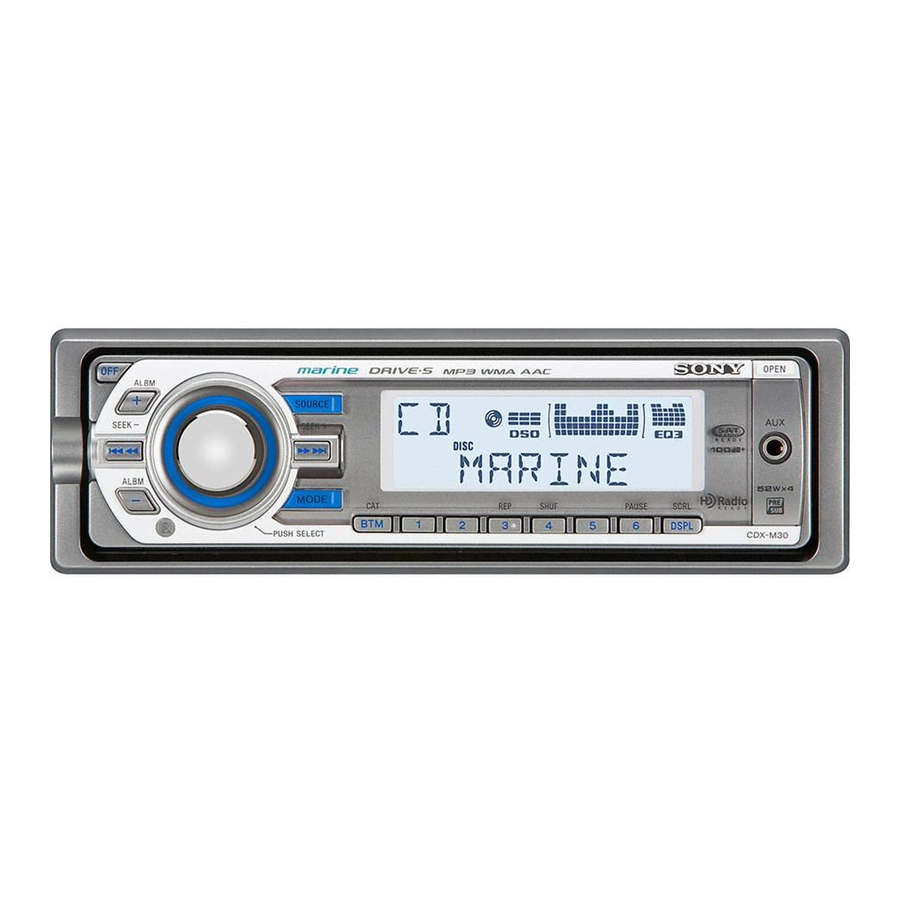
Page 5: General
CDX-M30 SECTION 2 GENERAL This section is extracted from instruction manual. • Location of controls and basic operations Location of controls and basic operations Main unit J MODE button page 11 This section contains instructions on the location of controls and basic operations. For details, see To select the radio band* ;... - Page 6 CDX-M30 Source selector (not supplied) Sélecteur de source (non fourni) Selector de fuente Supplied with the CD/MD changer (no suministrado) Fourni avec le changeur CD/MD Signalquellenwähler Suministrado con el cambiador de CD/MD (nicht mitgeliefert) Mit dem CD/MD-Wechsler geliefert Geluidsbronkiezer Geleverd met de CD/MD-wisselaar...
-
Page 7: Disassembly
CDX-M30 SECTION 3 DISASSEMBLY Note: This set can be disassemble according to the following sequence. 3-1. SUB (AUX) PANEL ASSY (Page 8) 3-2. CD MECHANISM BLOCK (Page 8) 3-4. SERVO BOARD 3-3. MAIN BOARD (Page 9) (Page 9) 3-5. CHASSIS (T) SUB ASSY (Page 10) 3-6. -
Page 8: Sub (Aux) Panel Assy
CDX-M30 Note: Follow the disassembly procedure in the numerical order given. 3-1. SUB (AUX) PANEL ASSY 3 two claws 2 two claws 4 flexible flat cable (17 core) 1 two screws (CN702) (+PTT 2.6 × 6) 5 sub (AUX) panel assy 3-2. -
Page 9: Main Board
CDX-M30 3-3. MAIN BOARD 4 screw 5 two screws (+PTT 2.6 × 10) (+P 2.6 × 8) 6 two screws (+PTT 2.6 × 10) 7 two screws (+P 2.6 × 8) 1 three ground point screws (+PTT 2.6 × 6) 2 two screws (+PTT 2.6 ×... -
Page 10: Chassis (T) Sub Assy
CDX-M30 3-5. CHASSIS (T) SUB ASSY 2 two precision screws 1 two precision screws (+P 1.7 × 2.2) (+P 1.7 × 2.2) 4 chassis (T) sub assy 3 claw 3-6. ROLLER ARM ASSY 5 roller arm assy 4 gear (RA1) -
Page 11: Chassis (Op) Assy
CDX-M30 3-7. CHASSIS (OP) ASSY 6 chassis (OP) assy 1 tension spring (KF) 7 coil spring (damper) (natural) 8 coil spring (damper) (blue) 4 slider (R) 3 lever (D) 2 gear (LE1) 3-8. CHUCKING ARM SUB ASSY 3 chucking arm sub assy 1 spring Note: Have this portion receive the chassis. -
Page 12: Sled Motor Assy
CDX-M30 3-9. SLED MOTOR ASSY 2 three serration screws (M 2 × 3) 3 sled motor assy 1 spring turn table spring stand Note: Never remove these parts since they were adjusted. stand Note: Place the stand with care not to touch the turn table. -
Page 13: Optical Pick-Up Section
CDX-M30 3-10. OPTICAL PICK-UP SECTION 2 optical pick-up section Note: Be careful not to touch the lens and hologram terminal when removing the optical pick-up section. 3-11. OPTICAL PICK-UP 1 pan tapping screw (M 1.4 × 2.5) 2 leaf spring (sub guide) -
Page 14: Diagnosis Function
CDX-M30 SECTION 4 DIAGNOSIS FUNCTION Description of the Diagnostics function: 4. Contents of each display mode 4-1. Reset count display mode 1. Setting the Diag display mode With the power off, press the [4/SHUF] button, [5] button, and [4/SHUF] button on the set body or the remote control (for more than 2 seconds) in turn. - Page 15 CDX-M30 4-4. Operating hours display mode 4-5-2. Disc type and operating hours Disc type Indication Disc type Operating hours Operating hours (in hexadecimal format) Disc type Diag code Recency of information 04: Operating hours ATRAC 1 - 3: 1 represents the latest.
- Page 16 CDX-M30 4-6. OFFSET/FAILURE error display mode Operating hours Error description (0: OFFSET, 1: FAILURE) Recency of information 1 - 3: 1 represents the latest. Diag code 06: OFFSET/FAILURE The display mode is switched by each rotation of [ALBM +] or [ALBM --] buttons during the OFFSET/FAILURE error display mode.
-
Page 17: Diagrams
CDX-M30 SECTION 5 DIAGRAMS 5-1. BLOCK DIAGRAM — MAIN SECTION — J451 (2/2) ELECTRONIC VOLUME IC401 FRONT AUDIO OUT J451 (1/2) R-CH 2 A2 R-CH 1 A1 AUDIO OUTS2 R-CH OUTS1 REAR/SUB AUDIO OUT R-CH (REAR/SUB) R-CH MUTE POWER AMP, MULTI... -
Page 18: Block Diagram -Display Section
CDX-M30 5-2. BLOCK DIAGRAM — DISPLAY SECTION — THIS NOTE IS COMMON FOR PRINTED WIRING BOARDS AND SCHEMATIC DIAGRAMS. (In addition to this, the necessary note is printed in each block.) SYSTEM CONTROL LCD DRIVER/LED CONTROL IC501 (2/2) IC901 for schematic diagram:... -
Page 19: Printed Wiring Board -Main Section
CDX-M30 5-3. PRINTED WIRING BOARD — MAIN SECTION — : Uses unleaded solder. J451 • Semiconductor J370 Location CNJ400 Ref. No. Location CN300 D101 JW123 D102 C442 C422 C432 C452 C323 C324 C414 C413 D103 FU601 D104 R432 R452 R442... -
Page 20: Schematic Diagram -Main Section (1/3)
CDX-M30 5-4. SCHEMATIC DIAGRAM — MAIN SECTION (1/3) — • Refer to page 26 for IC Block Diagrams. C323 C303 C306 C324 C308 C317 JC302 JC300 JC301 C301 C309 R302 JC504 C319 C304 C305 C307 R301 C318 IC300 IC B/D... -
Page 21: Schematic Diagram -Main Section (2/3)
CDX-M30 5-5. SCHEMATIC DIAGRAM — MAIN SECTION (2/3) — • Refer to page 26 for IC Block Diagrams. J451 C432 C413 C414 C442 C422 C452 R418 R416 R442 R422 R452 R432 C443 C447 R419 R417 JC303 R474 C423 C446 C494... -
Page 22: Schematic Diagram -Main Section (3/3)
CDX-M30 5-6. SCHEMATIC DIAGRAM — MAIN SECTION (3/3) — • Refer to page 18 for Waveforms and page 27 for IC Pin Description. (Page 20) (Page 21) Q590 IC502 C519 D493 R543 Q589 S103 JC53 IC602 C501 C325 C502 R494... -
Page 23: Printed Wiring Board -Sub Section
CDX-M30 5-7. PRINTED WIRING BOARD — SUB SECTION — 5-8. SCHEMATIC DIAGRAM — SUB SECTION — : Uses unleaded solder. (Page 24) CN202 CN201 LED202 R201 R202 R202 CN201 R201 S201 (Page 22) (Page 25) LED201 LED202 LED201 S201 (Page 19) -
Page 24: Printed Wiring Board -Display Section
CDX-M30 5-9. PRINTED WIRING BOARD — DISPLAY SECTION — : Uses unleaded solder. LED908 S901 LED958 D982 LED930 LED949 LED950 LED931 LCD901 LED947 LED951 S903 S906 LED906 LED956 S905 S915 S911 S909 S913 S912 S910 S908 S914 IC971 • Semiconductor Location Ref. -
Page 25: Schematic Diagram -Display Section
CDX-M30 5-10. SCHEMATIC DIAGRAM — DISPLAY SECTION — R981 D982 R977 R982 LED915 LED965 LED911 LED961 LED948 LED946 LED902 LED952 LED908 LED958 IC971 R978 LED931 LED913 LED963 LED909 LED959 LED943 LED993 LED905 LED955 LED907 LED957 R979 C971 LED916 LED966 LED912... - Page 26 CDX-M30 • IC Block Diagrams IC300 TDA8588AJ/N2/R1 (MAIN BOARD (1/3)) IC601 BA8271F-E2 (MAIN BOARD (1/3)) IC401 BD3442FS-E2 (MAIN BOARD (2/3)) BUS ON BUS.ON SWITCH VCC2 32 FIL LF– C BUS RESET 100k SWITCH 31 GND BUS.IN CLK-IN BATTERY INPUT INPUT...
- Page 27 CDX-M30 • IC Pin Description IC501 MB90F045PF-G-9060-SPE1 (SYSTEM CONTROL) (MAIN BOARD (3/3)) Pin No. Pin Name Pin Description AREASEL0 Destination setting pin (Fixed at L in this set) AREASEL1 Destination setting pin (Fixed at L in this set) AREASEL2 Destination setting pin (L: FM (50k)/AM (9k), H: FM (200k)/AM (10k))
- Page 28 Not used. (Open) RDS data block synchronized detection signal input from RDS receiver IC. DAVN (Fixed at L in this set) Not used. (Open) UNISI SONY-BUS data signal input UNISO SONY-BUS data signal output UNISCK SONY-BUS clock signal output 61 to 63 Not used.
-
Page 29: Exploded Views
CDX-M30 SECTION 6 EXPLODED VIEWS NOTE: • The mechanical parts with no reference • -XX and -X mean standardized parts, so The components identified by mark 0 or dotted line with mark number in the exploded views are not supplied. -
Page 30: Front Panel Section
CDX-M30 6-2. FRONT PANEL SECTION RE901 not supplied LCD901 not supplied (KEY board) J901 not supplied not supplied not supplied not supplied Ref. No. Part No. Description Remark Ref. No. Part No. Description Remark A-1313-113-A PANEL OVERALL ASSY, FRONT 3-250-543-21 SCREW (+B P-TITE M2) -
Page 31: Cd Mechanism Section (Mg-101Fc-188//Q)
CDX-M30 6-3. CD MECHANISM SECTION (MG-101FC-188//Q) not supplied not supplied not supplied not supplied not supplied not supplied not supplied not supplied not supplied not supplied not supplied Ref. No. Part No. Description Remark Ref. No. Part No. Description Remark A-1289-450-A MECHANICAL BLOCK ASSY (08) 3-348-998-31 SCREW (M1.4X2.5), TAPPING, PAN... -
Page 32: Electrical Parts List
CDX-M30 SECTION 7 ELECTRICAL PARTS LIST NOTE: • Due to standardization, replacements in • Items marked “*” are not stocked since The components identified by mark 0 or dotted line with mark the parts list may be different from the they are seldom required for routine service. - Page 33 CDX-M30 MAIN Ref. No. Part No. Description Remark Ref. No. Part No. Description Remark LED965 6-501-547-01 LED CL-197HB1E-D-T (1) R953 1-216-031-00 RES-CHIP 1/10W LED966 6-501-547-01 LED CL-197HB1E-D-T (BTM/CAT) R954 1-216-037-00 RES-CHIP 1/10W LED993 6-501-547-01 LED CL-197HB1E-D-T R955 1-216-029-00 RES-CHIP 1/10W...
- Page 34 CDX-M30 MAIN Ref. No. Part No. Description Remark Ref. No. Part No. Description Remark 1-126-947-11 ELECT 47uF C423 1-165-908-11 CERAMIC CHIP 1-162-970-11 CERAMIC CHIP 0.01uF C431 1-126-964-11 ELECT 10uF 1-162-967-11 CERAMIC CHIP 0.0033uF 10% C432 1-163-251-11 CERAMIC CHIP 100PF 1-162-970-11 CERAMIC CHIP 0.01uF...
- Page 35 CDX-M30 MAIN Ref. No. Part No. Description Remark Ref. No. Part No. Description Remark < DIODE > IC401 6-710-065-01 IC BD3442FS-E2 IC501 6-807-655-01 IC MB90F045PF-G-9060-SPE1 6-501-734-01 DIODE MAZ8056GMLS0 IC502 6-711-653-01 IC S-1206B33-U3T1G D101 6-501-743-01 DIODE MAZ8068GMLS0 IC601 6-703-884-01 IC BA8271F-E2...
- Page 36 CDX-M30 MAIN Ref. No. Part No. Description Remark Ref. No. Part No. Description Remark Q491 8-729-027-23 TRANSISTOR DTA114EKA-T146 R472 1-216-833-11 METAL CHIP 1/10W Q492 8-729-027-43 TRANSISTOR DTC114EKA-T146 R474 1-216-864-11 SHORT CHIP Q501 8-729-027-23 TRANSISTOR DTA114EKA-T146 R480 1-216-827-11 METAL CHIP 3.3K...
- Page 37 CDX-M30 MAIN SERVO Ref. No. Part No. Description Remark Ref. No. Part No. Description Remark R558 1-216-809-11 METAL CHIP 1/10W < DIODE > R559 1-216-845-11 METAL CHIP 100K 1/10W R562 1-216-845-11 METAL CHIP 100K 1/10W LED201 8-719-053-09 LED SML-310VTT86 (DISC IN)
- Page 38 CDX-M30 REVISION HISTORY Clicking the version allows you to jump to the revised page. Also, clicking the version at the top of the revised page allows you to jump to the next revised page. Ver. Date Description of Revision 2007. 08...