Table of Contents
Advertisement
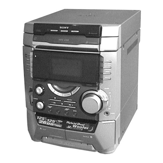
SERVICE MANUAL
Ver 1.2 2001.11
HCD-DX8 is the tuner, tape player, CD player
and amplifier section in MHC-DX8.
This stereo system is equipped with the Dolby B-
type noise reduction system*.
* Manufactured under license from Dolby
Laboratories Licensing Corporation.
DOLBY and the double-D symbol ; are
trademarks of Dolby Laboratories Licensing
Corporation.
Amplifier section
The following measured at AC 120, 220, 240V
50/60 Hz
DIN power output (rated) 160 + 160 watts
Continuous RMS power output (reference)
Inputs
MD/VIDEO (AUDIO) IN: voltage 450 mV/250 mV,
(phono jacks)
MIC:
(phone jack)
Outputs
PHONES:
(stereo mini jack)
FRONT SPEAKER:
SATELLITE SPEAKER:
Sony Corporation
9-929-221-13
2001K0500-1
Home Audio Company
C 2001.11
Published by Sony Engineering Corporation
Model Name Using Similar Mechanism
CD Mechanism Type
CD
SECTION
Base Unit Type
Optical Pick-up Type
Model Name Using Similar Mechanism
TAPE DECK
SECTION
Tape Transport Mechanism Type
SPECIFICATIONS
CD player section
System
Laser
(6 ohms at 1 kHz, DIN)
200 + 200 watts
(6 ohms at 1 kHz,
Laser output
10% THD)
impedance 47 kilohms
sensitivity 1 mV,
impedance 10 kilohms
Frequency response
Wavelength
accepts headphones of 8
Signal-to-noise ratio
ohms or more
Dynamic range
accepts impedance of 6 to
CD OPTICAL DIGITAL OUT
16 ohms
(Square optical connector jack, rear panel)
accepts impedance of 6 to
Wavelength
16 ohms
Output Level
COMPACT DISC DECK RECEIVER
HCD-DX8
Australian Model
HCD-BX7
CDM58-K2BD38
BU-K2BD38
KSM-213DAP/Z-NP
NEW
TCM-230AWR11
Compact disc and digital
audio system
Semiconductor laser
(λ=780nm)
Emission duration:
continuous
Max. 44.6 µ W*
*This output is the value
measured at a distance of
200 mm from the
objective lens surface on
the Optical Pick-up Block
with 7 mm aperture.
2 Hz – 20 kHz (±0.5 dB)
780 – 790 nm
More than 90 dB
More than 90 dB
660 nm
–18 dBm
— Continued on next page —
E Model
Advertisement
Table of Contents

Related Manuals for Sony HCD-DX8


Summary of Contents for Sony HCD-DX8
- Page 1 HCD-DX8 SERVICE MANUAL E Model Australian Model Ver 1.2 2001.11 HCD-DX8 is the tuner, tape player, CD player and amplifier section in MHC-DX8. This stereo system is equipped with the Dolby B- Model Name Using Similar Mechanism HCD-BX7 type noise reduction system*.
- Page 2 COMPONENTS IDENTIFIED BY MARK 0 OR DOTTED LINE WITH MARK 0 ON THE SCHEMATIC DIAGRAMS AND IN THE PARTS LIST ARE CRITICAL TO SAFE OPERATION. REPLACE THESE COMPONENTS WITH SONY PARTS WHOSE PART NUMBERS APPEAR AS SHOWN IN THIS MANUAL OR IN SUPPLEMENTS PUBLISHED BY SONY.
-
Page 3: Table Of Contents
TABLE OF CONTENTS NOTES ON HANDLING THE OPTICAL PICK-UP BLOCK OR BASE UNIT 1. SERVICE NOTE ······························································· 4 The laser diode in the optical pick-up block may suffer electrostatic 2. GENERAL ·········································································· 5 break-down because of the potential difference generated by the charged electrostatic load, etc. -
Page 4: Service Note
SECTION 1 SERVICE NOTE Note for installing the panel board 2 Panel board Hot melt : melted-connection point Screw hole 1 Cut the nine melted-connection points with cutting pliers. Attach the panel board with six screws (+BVTP 2.6 × 8 ) after the board is removed once. -
Page 5: General
SECTION 2 GENERAL LOCATION OF CONTROLS • Front view 2 3 4 DISC SKIP button DISC 1 button and indicator DISC 2 button and indicator DISC 3 button and indicator Z OPEN/CLOSE button CD disc tray Fluorescent indicator tube EDIT, TUNER, MEMORY button PLAY MODE, STEREO/MONO button REPEAT, DOLBY NR button qgqh... - Page 6 This section is extracted from instruction manual. Step 3: Setting the Press ENTER. The minute indication flashes. time You must set the time before using the timer functions. Press . or > repeatedly to set the minute. Press ENTER. The clock starts working. If you’ve made a mistake, start over from step 1.
-
Page 7: Disassembly
SECTION 3 DISASSEMBLY Note: Follow the disassembly procedure in the numerical order given. CASE (TOP) 7 two screws 9 case (top) (BVTP3 × 10) 4 three screws (case) 5 two screws (BVTP3 × 10) 8 claw 3 side panel R 6 side panel L 2 two screws (BVTP3 ×... - Page 8 FRONT PANEL ASS’Y 8 connector (19 core) (CN201) q; CD mechanism deck 4 screw (BVTP3 × 10) 5 connector (CN601) 1 wire (flat type) (17 core) (CN304) 4 screw (BVTP3 × 10) BASE UNIT (Page 11) DRIVER/MOTOR/ SENSOR BOARDS (Page 11) 2 connector (CN1) 9 connector (CN202) 2 connector (CN2)
- Page 9 PANEL BOARD 7 three claws q; five claws 5 knob (MIC) 6 two screws (BVTP2.6 × 8) 5 knob (MIC) 8 CD switch board 2 two screws (BVTP2.6 × 8) : melted-connection point 9 Cut the nine melted-connection points with a cutting plier. Note: When attching the panel board, qa PANEL board refer to "Service Note"...
- Page 10 MAIN/POWER AMP BOARDS 8 heat sink 5 three screws (BVTP3 × 8) 2 connector (CN503) 7 two screws (BVTP3 × 8) 2 connector (CN502) 6 POWER AMP board 3 MAIN board 4 two screws (BVTP3 × 16) 1 two screws (BVTP3 ×...
- Page 11 BASE UNIT (BU-K2BD38) 4 two insulators 3 Base unit 1 wire (flat type) (19 core) (CN101) 4 two insulators 2 four screws (PTPWH 2.6) DRIVER/MOTOR/SENSOR BOARDS q; screw (PTPWH2.6 × 8) 5 two screws (+BVTP 2.6 × 8) 9 MOTOR board 7 wire (flat type) (8 core) (CN721) 4 Remove the two solderings of motor.
-
Page 12: Test Mode
SECTION 4 TEST MODE [MC Cold Reset] [Change-over of AM Tuner Step between 9 kHz and • The cold reset clears all data including preset data stored in the 10 kHz] RAM to initial conditions. Execute this mode when returning •... - Page 13 [MC Test Mode] • This mode is used to check operations of the respective sections of Amplifier, Tuner, CD and Tape. Procedure: Press the ?/1 button to turn on the set. Press the three buttons of x , ENTER and DISC 3 simultaneously.
- Page 14 [Aging Mode] This mode can be used for operation check of CD section and tape deck section. • If an error occurred: The aging operation stops and display status. • If no error occurs: The aging operation continues repeatedly. 1. Operating method of Aging Mode Turn on the main power and select “CD”...
- Page 15 2) Operation during aging mode In the aging mode, the program is executed in the following sequence. (1) The disc tray opens and closes. (2) The mechanism accesses DISC 2 and makes an attempt to read TOC. However, since there are no discs, a message “CD2 NO DISC”...
-
Page 16: Mechanical Adjustments
SECTION 5 SECTION 6 MECHANICAL ADJUSTMENTS ELECTRICAL ADJUSTMENTS Precaution DECK SECTION 0 dB=0.775 V 1. Clean the following parts with a denatured alcohol-moistened swab: 1. Demagnetize the record/playback head with a head record/playback heads pinch rollers demagnetizer. erase head rubber belts 2. - Page 17 2. Turn the adjustment screw and check output peaks. If the peaks DECK B Tape Speed Adjustment do not match for L-CH and R-CH, turn the adjustment screw Note: Start the Tape Speed adjustment as below after setting to the test so that outputs match within 1dB of peak.
- Page 18 DECK B REC Bias Adjustment 4. Mode: Record Procedure: INTRODUCTION MD/VIDEO (AUDIO) IN When set to the test mode performed in Tape Speed Adjustment, 315 Hz, 50 mV (–23.8 dB) AF OSC when the tape is rewound after recording, the “REC memory mode” blank tape 600 Ω...
- Page 19 FM Tuned Level Adjustment CD SECTION FM RF SSG Note : 1. CD Block is basically designed to operate without adjustment. 75 Ω coaxial Therefore, check each item in order given. 2. Use YEDS-18 disc (3-702-101-01) unless otherwise indicated. 3. Use an oscilloscope with more than 10MΩ impedance. 4.
- Page 20 Note: Clear RF signal waveform means that the shape “◊” can be Adjustment Location: clearly distinguished at the center of the waveform. [BD BOARD] (Conductor side) RF signal waveform TP (VC) VOLT/DIV : 200mV TP (TEO) TIME/DIV : 500ns TP (RF) TP (FEO) level : 1.45 ±...
-
Page 21: Diagrams
HCD-DX8 SECTION 7 DIAGRAMS 7-1. CIRCUIT BOARDS LOCATION THIS NOTE IS COMMON FOR PRINTED WIRING BOARDS AND SCHEMATIC DIAGRAMS. (In addition to this, the necessary note is printed in each block.) MOTOR board DRIVER board Note on Schematic Diagram: Note on Printed Wiring Boards: •... -
Page 22: Block Diagrams
HCD-DX8 7-2. BLOCK DIAGRAMS – TUNER/CD SECTION – TM601 FE602 AM/FM IF MPX ANTENNA FM FRONT-END LPF601 Q601 IC601 CF601 CF602 BUFFER L-CH • R-CH: Same as L-CH. ANT IN IF OUT FM IF L OUT FM 75Ω Q611 • Signal Path... - Page 23 HCD-DX8 – MAIN SECTION – GRAPHIC EQUALIZER CONTROL, DBFB ELECTRICAL VOLUME IC101 IC102 IC501 TM801 TUNER L-CH SECTION IN2A VOL OUT2 (Page 22) POWER SPEAKER Q504,505 Q861 Q821,822 IMPEDANS USE 6-16 Ω RY801 Q824,825 R CH CD-L MUTE MUTE MUTE...
-
Page 24: Printed Wiring Board - Bd Section
HCD-DX8 7-3. PRINTED WIRING BOARD – BD SECTION – • See page 21 for Circuit Boards Location. • Semiconductor Location Ref. No. Location IC101 IC102 IC103 Q101 TP (VC) TP (TEO) TP (FEO) TP (RF) TP (FEI) TP (AGCCON) (XPCK) -
Page 25: Schematic Diagram - Bd Section
HCD-DX8 7-4. SCHEMATIC DIAGRAM – BD SECTION – • See page 21 for Waveforms. • See page 42 for IC Block Diagrams. (Page 29) The components identified by mark 0 or dotted • Voltages and waveforms are dc with respect to ground line with mark 0 are critical for safety. -
Page 26: Printed Wiring Board - Main Section
HCD-DX8 • Semiconductor 7-5. PRINTED WIRING BOARD – MAIN SECTION – • See page 21 for Circuit Boards Location. Location (Page 36) (Page 24) Ref. No. Location D501 D502 D503 D504 D505 D506 D508 D511 D601 D641 D-11 D651 D801... -
Page 27: Schematic Diagram - Main (1/3) Section
HCD-DX8 7-6. SCHEMATIC DIAGRAM – MAIN (1/3) SECTION – • See page 42 for IC Block Diagrams. • Voltages and waveforms are dc with respect to ground under no-signal (detuned) conditions. no mark : FM ) : AM (Page 29) -
Page 28: Schematic Diagram - Main (2/3) Section
HCD-DX8 7-7. SCHEMATIC DIAGRAM – MAIN (2/3) SECTION – • See page 21 for Waveforms. • See page 42 for IC Block Diagrams. (Page 29) (Page 29) (Page 29) (Page 35) • Voltages and waveforms are dc with respect to ground under no-signal conditions. -
Page 29: Schematic Diagram - Main (3/3) Section
HCD-DX8 7-8. SCHEMATIC DIAGRAM – MAIN (3/3) SECTION – (Page 31) (Page 31) (Page 27) (Page 25) (Page 37) (Page 28) (Page 28) • Voltages and waveforms are dc with respect to ground under no-signal conditions. The components identified by mark 0 or dotted... -
Page 30: Printed Wiring Board - Power Amp Section
HCD-DX8 7-9. PRINTED WIRING BOARD – POWER AMP SECTION – (Page 26) (Page 26) • See page 21 for Circuit Boards Location. • Semiconductor Location Ref. No. Location D501 D502 D503 D504 D541 D543 D551 D581 D941 D979 IC501 Q501... -
Page 31: Schematic Diagram - Power Amp Section
HCD-DX8 7-10. SCHEMATIC DIAGRAM – POWER AMP SECTION – (Page 39) (Page 39) (Page 29) (Page 29) The components identified by mark 0 or dotted • Voltages and waveforms are dc with respect to ground line with mark 0 are critical for safety. -
Page 32: Printed Wiring Boards - Panel Section
HCD-DX8 7-11. PRINTED WIRING BOARDS – PANEL SECTION – • See page 21 for Circuit Boards Location. • Semiconductor Location – CD SWITCH BOARD – Ref. No. Location D630 D631 D632 Q630 Q631 Q632 Q633 Q634 Q635 • Semiconductor Location –... -
Page 33: Schematic Diagram - Panel Section
HCD-DX8 7-12. SCHEMATIC DIAGRAM – PANEL SECTION – • See page 21 for Waveform. • See page 42 for IC Block Diagrams. (Page 29) • Voltages and waveforms are dc with respect to ground under no-signal conditions. no mark : CD STOP... -
Page 34: Printed Wiring Boards - Leaf Sw Section
HCD-DX8 7-13. PRINTED WIRING BOARDS – LEAF SW SECTION – • See page 21 for Circuit Boards Location. (Page 26) (Page 26) (Page 26) -
Page 35: Schematic Diagram - Leaf Sw Section
HCD-DX8 7-14. SCHEMATIC DIAGRAM – LEAF SW SECTION – (Page 28) • Voltages and waveforms are dc with respect to ground under no-signal conditions. no mark : PB (DECK- A) ) : PB (DECK- B) -
Page 36: Printed Wiring Boards - Driver Section
HCD-DX8 7-15. PRINTED WIRING BOARDS – DRIVER SECTION – • See page 21 for Circuit Boards Location. • Semiconductor Location Ref. No. Location D701 IC701 IC711 (BU UP/DOWN) (Page 26) CN202... -
Page 37: Schematic Diagram - Driver Section
HCD-DX8 7-16. SCHEMATIC DIAGRAM – DRIVER SECTION – • See page 42 for IC Block Diagram. (Page 29) • Voltages and waveforms are dc with respect to ground under no-signal conditions. no mark : CD (STOP) -
Page 38: Printed Wiring Board - Trans Section
HCD-DX8 7-17. PRINTED WIRING BOARD – TRANS SECTION – • See page 21 for Circuit Boards Location. (Page 30) (Page 30) -
Page 39: Schematic Diagram - Trans Section
HCD-DX8 7-18. SCHEMATIC DIAGRAM – TRANS SECTION – (Page 31) (Page 31) The components identified by mark 0 or dotted line with mark 0 are critical for safety. Replace only with part number specified. -
Page 40: Ic Pin Function Description
HCD-DX8 7-19. IC PIN FUNCTION DESCRIPTION • IC401 SYSTEM CONTROLLER (M30622MAA-A60) (MAIN BOARD) Pin No. Pin Name Description Pin No. Pin Name Description FREQ-B Sound control signal to the satellite amplifier (TA-DX8). SURROUND 1 Surround control signal output. Not used. - Page 41 • IC601 DISPLAY CONTROLLER (TMP88CP77F-1A22) (PANEL BOARD) Pin No. Pin Name Description VOL A VOLUME A signal input. VOL B VOLUME B signal input. HEADPHONE Headphone detect signal input. H=ON, L=OFF Not used. EXIST3 LED EXIST LED of disc3 drive signal output. PLAY3 LED PLAY LED of disc3 drive signal output.
-
Page 42: Ic Block Diagrams
7-20. IC BLOCK DIAGRAMS – BD Board – IC101 CXD2587Q ERROR DIGITAL CORRECTOR DIGITAL ASYMMETRY CORRECTION OPERATIONAL LRCK AMPLIFIER ANALOG SWITCH PCMD INTERFACE DEMODULATOR CONVERTER EMPH XVDD XTAI TIMING CLOCK LOGIC XTAO XTSL GENERATOR XVSS TES1 AVDD1 TEST AOUT1 SERVO DSP PWM GENERATOR AIN1 FRDR... - Page 43 IC103 CXA2568M-T6 HOLD APC PD AMP LC/PD APC LD AMP – LD ON – – – HOLD SW AGC CONT AGC VTH 50µA RF BOT – – – – RFTC RF SUMMING AMP RF EQ AMP RF I RF O –...
-
Page 44: Main Board
– MAIN Board – IC302 µPC1330HA INVERTER COMPARATER SW P1 CONT GND SW P2 GND SW R1 GND SW R2 IC601 BA1450 AM IF VREG DECODER DRIVER COMP... -
Page 45: Panel Board
IC651 LC72130 PHASE DETECTOR CHARGE PUMP UNLOCK POWER DETECTOR RESET REFERENCE SWALLOW COUNTER DIVIDER 1/16, 1/17 4BITS 12BITS PROGRAMMABLE DRIVER UNIVERSAL DATA SHIFT REGISTER LATCH COUNTER 3 4 5 6 – PANEL Board – IC602 BA3830F-E2 IC721 M65850FP (EA model only) REFFERENCE RESET 18 RESET... -
Page 46: Exploded Views
SECTION 8 EXPLODED VIEWS NOTE: • -XX and -X mean standardized parts, so they • Items marked “*” are not stocked since they The components identified by mark 0 or dotted line with mark may have some difference from the original are seldom required for routine service. - Page 47 4-225-032-01 VOL KNOB 4-225-053-01 SPRING R A-4473-082-A PANEL BOARD, COMPLETE (EXCEPT EA) A-4428-077-A CD SWITCH BOARD, COMPLETE A-4473-084-A PANEL BOARD, COMPLETE (EA) 4-962-708-71 EMBLEM (4-A), SONY 4-951-620-01 SCREW (2.6X8), +BVTP 4-225-033-01 FR KNOB 4-224-578-01 KNOB (MIC) X-4952-667-1 FRONT PANEL ASSY (E3)
- Page 48 (3) CHASSIS SECTION not supplied T971 E2, E3 not supplied AR, MX EA, MY, EA, MY, SP The components identified by mark 0 or dotted line with mark 0 are critical for safety. Replace only with part number specified. Ref. No. Part No.
- Page 49 Ver 1.1 (4) TAPE MECHANISM DESK SECTION (TCM-230AWR11) M901 HP901 supplied not supplied supplied HRPE901 Ref. No. Part No. Description Remark Ref. No. Part No. Description Remark X-3374-156-5 PINCH LEVER (REV) ASSY X-3378-041-1 FLYWHEEL (A-REV) ASSY X-3374-155-5 PINCH LEVER (FWD) ASSY X-3378-040-1 FLYWHEEL (A-FWD) ASSY A-2007-839-A HEAD (A) BOARD, COMPLETE X-3378-043-1 FLYWHEEL (B-REV) ASSY...
- Page 50 Ver 1.2 (5) CD MECHANISM DESK SECTION (CMD58-K2BD38) M721 not supplied not supplied BU-K2BD38 not supplied Ref. No. Part No. Description Remark Ref. No. Part No. Description Remark 4-933-134-11 SCREW (+PTPWH M2.6X8) 4-221-688-01 PULLEY (B), CHUCKING 4-221-679-01 CAM (RELAY) 1-471-035-11 MAGNET ASSY 4-221-675-01 TABLE X-4952-019-1 PULLEY (A) ASSY, CHUCKING 4-221-686-01 LEVER (CHANGE)
- Page 51 (6) BASE UNIT SECTION (BU-K2BD38) The components identified by mark 0 or dotted line with mark 0 are critical for safety. Replace only with part number specified. Ref. No. Part No. Description Remark Ref. No. Part No. Description Remark 0 251 8-820-116-01 OPTICAL PICK UP KSM-213DAP/Z-NP A-4724-934-A BD BOARD, COMPLETE 1-792-024-11 WIRE (FLAT TYPE) (16 CORE)
-
Page 52: Electrical Parts List
SECTION 9 ELECTRICAL PARTS LIST NOTE: • Due to standardization, replacements in the • Items marked “*” are not stocked since they The components identified by mark 0 or dotted line with mark are seldom required for routine service. parts list may be different from the parts speci- 0 are critical for safety. - Page 53 CD SWITCH DRIVER HEAD (A) HEAD (B) LEAF SW Ref. No. Part No. Description Remark Ref. No. Part No. Description Remark R124 1-216-097-00 RES-CHIP 100K 1/10W S644 1-771-410-21 SWITCH, TACTILE (DISC 2) R131 1-216-033-00 METAL CHIP 1/10W S645 1-771-410-21 SWITCH, TACTILE (DISC 3) S646 1-771-410-21 SWITCH, TACTILE (Z OPEN/CLOSE (CD)) R143...
- Page 54 LEAF SW MAIN Ref. No. Part No. Description Remark Ref. No. Part No. Description Remark < TRANSISTOR > C124 1-163-038-00 CERAMIC CHIP 0.1uF Q1001 8-729-029-56 TRANSISTOR DTA144ESA-TP C125 1-126-964-11 ELECT 10uF C131 1-136-169-00 MYLAR 0.22uF < RESISTOR > C132 1-126-964-11 ELECT 10uF C133 1-126-925-11 ELECT...
- Page 55 MAIN Ref. No. Part No. Description Remark Ref. No. Part No. Description Remark C318 1-126-964-11 ELECT 10uF C414 1-163-038-00 CERAMIC CHIP 0.1uF C319 1-126-961-11 ELECT 2.2uF C416 1-126-916-11 ELECT 1000uF 6.3V C320 1-126-961-11 ELECT 2.2uF C321 1-163-131-00 CERAMIC CHIP 390PF C462 1-104-665-11 ELECT 100uF...
- Page 56 MAIN Ref. No. Part No. Description Remark Ref. No. Part No. Description Remark D510 8-719-988-61 DIODE 1SS355TE-17 C663 1-163-031-11 CERAMIC CHIP 0.01uF D511 8-719-988-61 DIODE 1SS355TE-17 C669 1-163-031-11 CERAMIC CHIP 0.01uF C803 1-163-031-11 CERAMIC CHIP 0.01uF D601 8-719-056-83 DIODE UDZ-TE-17-6.8B C821 1-104-665-11 ELECT 100uF...
- Page 57 MAIN Ref. No. Part No. Description Remark Ref. No. Part No. Description Remark < IF TRANSFORMER > JR923 1-216-295-00 SHORT IFT601 1-435-295-11 TRANSFORMER, IF JR924 1-216-295-00 SHORT JR928 1-216-295-00 SHORT < JACK > < COIL/SHORT > J101 1-793-987-11 JACK, PIN 2P (MD/VIDEO (AUDIO)) L201 1-414-189-31 INDUCTOR 100uH...
- Page 58 MAIN Ref. No. Part No. Description Remark Ref. No. Part No. Description Remark R302 1-216-057-00 METAL CHIP 2.2K 1/10W Q892 8-729-620-05 TRANSISTOR 2SC2603TP-EF R303 1-216-025-00 RES-CHIP 1/10W Q911 8-729-141-83 TRANSISTOR 2SB1375 R304 1-216-025-00 RES-CHIP 1/10W Q912 8-729-113-13 TRANSISTOR FA1A4M-T1L33 R305 1-216-057-00 METAL CHIP 2.2K 1/10W...
- Page 59 MAIN Ref. No. Part No. Description Remark Ref. No. Part No. Description Remark R497 1-216-081-00 METAL CHIP 1/10W R377 1-216-089-00 RES-CHIP 1/10W (E2, MX, AR) R378 1-216-094-00 RES-CHIP 1/10W R497 1-216-295-00 SHORT 0 (E3, MY, SP, AUS) R381 1-216-099-00 METAL CHIP 120K 1/10W R498...
- Page 60 MAIN MOTOR PANEL Ref. No. Part No. Description Remark Ref. No. Part No. Description Remark R667 1-216-222-00 RES-CHIP 1/8W < TRANSFORMER > R668 1-216-049-11 RES-CHIP 1/10W R669 1-216-065-00 RES-CHIP 4.7K 1/10W T301 1-423-980-11 TRANSFORMER, BIAS OSCILLATION T601 1-435-195-11 TRANSFORMER, DISCRIMINATOR R804 1-216-089-00 RES-CHIP 1/10W...
- Page 61 PANEL Ref. No. Part No. Description Remark Ref. No. Part No. Description Remark C652 1-126-960-11 ELECT C741 1-124-463-00 ELECT 0.1uF C653 1-126-960-11 ELECT C742 1-162-215-31 CERAMIC 47PF C654 1-164-159-11 CERAMIC 0.1uF C743 1-162-290-31 CERAMIC 470PF C744 1-162-294-31 CERAMIC 0.001uF C655 1-162-282-31 CERAMIC 100PF C656...
- Page 62 PANEL Ref. No. Part No. Description Remark Ref. No. Part No. Description Remark D614 8-719-071-41 LED SELS5923C-TP15 (V-GROOVE) R609 1-249-429-11 CARBON 1/4W D615 8-719-072-82 LED SELU5E20C-STP15 (FUNCTION) R610 1-247-807-31 CARBON 1/4W D617 8-719-063-93 LED SLR325VC-N-T32 (REC PAUSE/START) R611 1-249-429-11 CARBON 1/4W R612 1-249-401-11 CARBON...
- Page 63 PANEL POWER AMP Ref. No. Part No. Description Remark Ref. No. Part No. Description Remark R680 1-249-410-11 CARBON 1/4W < SWITCH > R681 1-249-411-11 CARBON 1/4W R682 1-249-413-11 CARBON 1/4W S601 1-418-725-11 ENCODER, ROTARY (12 TYPE) (VOLUMUE) R683 1-249-414-11 CARBON 1/4W S611 1-771-410-21 SWITCH, TACTILE (f)
- Page 64 POWER AMP SENSOR Ref. No. Part No. Description Remark Ref. No. Part No. Description Remark 0 R511 C552 1-162-294-31 CERAMIC 0.001uF 1-212-881-11 FUSIBLE 1/4W F 0 R512 C553 1-162-286-31 CERAMIC 220PF 1-202-972-61 FUSIBLE 1/4W F C554 1-104-665-11 ELECT 100uF R513 1-249-435-11 CARBON 1/4W C557...
- Page 65 Ver 1.1 TRANS Ref. No. Part No. Description Remark Ref. No. Part No. Description Remark 1-676-808-11 TRANS BOARD ************** HARDWARE LIST ************* ************** 1-533-293-11 FUSE HOLDER 7-628-254-05 SCREW +PS 2.6X5 < CAPACITOR > 7-685-646-79 SCREW +BVTP 3X8 TYPE2 N-S 7-685-647-79 SCREW +BVTP 3X10 TYPE2 N-S 0 C972 1-113-925-11 CERAMIC 0.01uF...
- Page 66 HCD-DX8 REVISION HISTORY Clicking the version allows you to jump to the revised page. Also, clicking the version at the upper right on the revised page allows you to jump to the next revised page. Ver. Date Description of Revision 2001.11...