Panasonic SA-AK18 Service Manual
Hide thumbs
Also See for SA-AK18:
- Service manual (120 pages) ,
- Wiring diagrams (40 pages) ,
- Operating instructions manual (32 pages)
Table of Contents
Advertisement
Specifications
AMPLIFIER SECTION (GC area)
PMPO
RMS power output
THD 10%, both channels driven
Input sensitivity
AUX
MIC
Input Impedance
AUX
MIC
AMPLIFIER SECTION (GN area)
RMS power output
THD 10%, both channels driven
Input sensitivity
AUX
Input Impedance
AUX
FM TUNER SECTION
Frequency range
Sensitivity
S/N 26 dB
Antenna terminal(s)
1400 W
70 W per channel (6 Ω)
250 mV
0.7 mV
13.9 kΩ
680 Ω
60 W per channel (6 Ω)
250 mV
13.9 kΩ
87.5 - 108 MHz (50 kHz steps)
2.5 µV (IHF)
2.2 µV
75 Ω (unbalanced)
SA-AK18
Colour
(S)... Silver Type
Area
(GC)...Asia, Latin America, Africa and Middle Near East
(GN)...Oceania
TAPE SECTION :
AR2 MECHANISM SERIES
CD SECTION :
RAE0152Z-3 TRAVERSE DECK SERIES
AM TUNER SECTION (GC area)
Frequency range
MW
SW
Sensitivity
MW
S/N 20 dB (at 999 kHz)
SW
S/N 20 dB (at 5.3 MHz)
AM TUNER SECTION (GN area)
Frequency range
Sensitivity
S/N 20 dB (at 999 kHz)
Track system
Heads
Record/playback
Erasure
Motor
© 2000 Matsushita Electronics (S) Pte Ltd. All rights
reserved. Unauthorized copying and distribution is a
violation of law.
ORDER NO. MD0004055C3
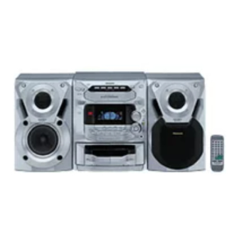
CD Stereo System
522 - 1629 kHz (9 kHz steps)
520 - 1630 kHz (10 kHz steps)
3.200 - 7.350 MHz (0.005 MHz
steps)
9.400 - 21.750 MHz (0.005 MHz
steps)
560 µV/m
35.5 µV/m
522 - 1629 kHz (9 kHz steps)
560 µV/m
4 track, 2 channel
Solid permalloy head
Double gap ferrite head
DC servo motor
Advertisement
Table of Contents

Related Manuals for Panasonic SA-AK18


Summary of Contents for Panasonic SA-AK18
-
Page 1: Specifications
ORDER NO. MD0004055C3 CD Stereo System SA-AK18 Colour (S)... Silver Type Area (GC)...Asia, Latin America, Africa and Middle Near East (GN)...Oceania TAPE SECTION : AR2 MECHANISM SERIES CD SECTION : RAE0152Z-3 TRAVERSE DECK SERIES Specifications AMPLIFIER SECTION (GC area) AM TUNER SECTION (GC area) -
Page 2: Table Of Contents
6.9 kg Beam source/wave length Semiconductor laser/780 nm SYSTEM Number of channels Stereo SC-AK18 (GC) Music Center: SA-AK18 (GC) Frequency response 20 Hz - 20 kHz (+1, -2 dB) Speaker: SB-AK18 (GC) Wow and flutter Below measurable limit SC-AK18 (GN) -
Page 3: In The Box
SA-AK18 1 Before Repair and Adjustment Disconnect AC power, discharge Power Supply Capacitors C536, C545, C546, C548 and C555 through a 10 Ω, 5W resistor to ground. DO NOT SHORT-CIRCUIT DIRECTLY (with a screwdriver blade, for instance), as this may destroy solid state devices. -
Page 4: Handling Precautions For Traverse Deck
SA-AK18 4 Handling Precautions For Traverse Deck The laser diode in the traverse deck (optical pickup) may break Grounding for electrostatic breakdown prevention down due to potential difference caused by static electricity of 1. Human body grounding clothes or human body. - Page 5 SA-AK18 Maximale Strahlungsleistung der Lasereinheit :100W/VDE Die Strahlung an der Lasereinheit ist ungefährlich, wenn folgende Punkte beachtet werden: 1. Die Lasereinheit nicht zerlegen, da die Strahlung an der freigelegten Laserdiode gefährlich ist. 2. Den werkseitig justierten Einstellregler der Lasereinhit nicht verstellen.
-
Page 6: Operation Procedures
SA-AK18 6 Operation Procedures... -
Page 7: Remote Control Description
SA-AK18... -
Page 8: Precaution Of Laser Diode
SA-AK18 7 Operation Checks and Main Component Replacement Procedures “ATTENTION SERVICER” Some chassis components may have sharp edges. Be careful when disassembling and servicing. 1. This section describes procedures for checking the operation of the major printed circuit boards and replacing the main components. - Page 9 SA-AK18 • Checking for Power P.C.B. Step 5 Remove the wire at CP605 and CN309. Step 6 Release the 2 catches and remove the CD changer base together with the CD changer. • Checking for Main, Panel and Deck P.C.B...
- Page 10 SA-AK18 7.2. Main Component Replacement Procedures Note: 7.2.1. Replacement of the Traverse Deck Insert a short pin into the flexible cable for traverse unit. Step 1 Follow the procedures in ‘Disassembly of the Traverse • Installation of the CD servo P.C.B. after replacement Unit’...
- Page 11 SA-AK18 Step 6 Unsolder the terminals of Power Amp IC and replace 7.2.2. Replacement of the Power the respective component. Amplifier IC Step 1 Follow the procedures in ‘Checking Procedure for each major P.C.B.’ ( Step 1 - Step 6 ).
- Page 12 SA-AK18 7.3. Disassembly and assembly of the Traverse Unit Step 1 Push the lever from position A to B. Step 2 Pull the stopper (black) in the direction of arrow 1 and push the lever in the direction of arrow 2.
- Page 13 SA-AK18 7.4. Disassembly and assembly of the Disc Tray Step 5 Rotate the hexagonal wrench in the direction of arrow (clockwise), and then open the disc tray fully. Step 2 With lifting the claw in the direction of arrow 1, draw the clamp SW P.C.B.
- Page 14 SA-AK18 Step 8 With forcing the left guide bar manually because the left Step 3 Align the drive rack with the drive gear. guide bar interferes with claw, draw the disc tray. • Installation of the disc tray after replacement Step 1 Slide the drive rack fully in the direction of the arrow.
-
Page 15: Cd Mechanism Test
SA-AK18 8 Self-Diagnostic Function 8.1. Self-diagnostic display This unit is equipped with a self-diagnostic display function which, if a problem occurs, will display an error code corresponding to the problem. Use this function when performing maintenance on the unit. 8.2. -
Page 16: To Clear All Error Code
SA-AK18 4. Press “OPEN/CLOSE (5)” and wait until the tray is open. 5. Press “OPEN/CLOSE (1)” and remove the CD. 6. Press “OPEN/CLOSE (1)” to close the tray. 7. Press “ /TUNE MODE” to indicate Error Code. • If several problem exist, error code will change each time when “ /TUNE MODE” is pressed. (e.g. F15 → F26 → F16 ..etc). -
Page 17: Cd Test Mode Function
SA-AK18 10 CD Test Mode Function This CD test mode is provided to check CD unit without 10.2. CD Automatically Adjustment connecting to changer loading mechanism. This mode shall result indication operate CD PLAY with CD unit being connected only and CD Automatic Alignment result is shown on FL display. -
Page 18: Bias And Erase Voltage Check
SA-AK18 11.1.3. Bias and Erase Voltage Check 1. Set the unit “AUX” position. 2. Insert the Normal blank tape (QZZCRA) into DECK 2 and the unit to “REC” mode (use “ REC/STOP” key). 3. Measure and make sure that the output is within the standard value. - Page 19 SA-AK18 11.2.2. AM-RF Alignment SIGNAL GENERATOR OR SWEEP RADIO DIAL SETTING INDICATOR ADJUSTMENT REMARKS GENERATOR (ELECTRONIC (Shown in Fig.3) VOLTMETER CONNECTIONS FREQUENCY OSCILLOSCOPE) Fashion a loop of 522 kHz Tuning capacitor fully closed Headphones Jack (32Ω) Z152 (GC), Adjust for maximum output.
-
Page 20: Alignment Points
SA-AK18 11.3. Alignment Points Cassette Deck section Tuner section... -
Page 21: Illustration Of Ic's, Transistors And Diodes
SA-AK18 12 Illustration of IC’s, Transistors and Diodes M38199MF227 (100P) STK470-010A RSN3502B BU2090AF-E2 (16P) TA7291P M62433AFP (80P) LA1833NMNTLM (24P) MN662790RSC (80P) LC72131MDTRM (20P) AN7348STA-E1 (24P) BA4558FE2 (8P) M62457AFPE1 (16P) 0N2180RLC1 BA7755A M5218AP AN8839NSBE2 (28P) AN8739SBE2 2SA1309ARTA 2SC2058SPTA 2SK544F-AC 2SB1238QRTV2 2SC3940AQSTA... -
Page 22: Terminal Function Of Ics
SA-AK18 13 Terminal Function of ICs 13.1. IC701 (AN8839NSBE2) Servo Amplifier Pin No. Mark Function Pin No. Mark Function Tracking signal input 1 /RFDET NRFDET output (“L” : detection) Tracking signal input 2 PDOWN Power-down input Power supply OFTR OFTR output Focus signal input terminal 1 N.C. - Page 23 SA-AK18 Mark Function Mark Function EFM signal output CLVS Spindle servo phase synchronizing signal output PLL extraction clock output ("H" : CLV, "L" : rough servo) (fPCK = 4.321 MHz during normal playback) Sub-code checked output (“H” :OK, “L” :NG) VCOF2 VCO Loop filter for 33.8688...
- Page 24 SA-AK18 Mark Function Mark Function J_JOG_AB EQ Joy jog A-D detection EEDAT EEPROM data input input EECLK EEPROM chip select output CHG_AD1 (OPEN/CLAMP)Changer Power supply (-30V) switch A-D detection input 1 AVSS Analog Ground (0V) CHG_AD2 (POSITION/BOTTOM) VREF Reference for A-D...
-
Page 25: Block Diagram
SA-AK18 14 Block Diagram IC701 AN8839NSBE2 SERVO AMP OPTICAL PICKUP RFIN CSBRT SEMICONDUCTOR LASER OFTR DET. TENV Q701 OFTR OFTR LASER POWER DRIVE DET. /RFDET /RFDET DET. FEOUT VCBA Subtracter LDON PHOTO DETECTOR Vref VREF Subtracter VCBA N.C. DIGITAL AUDIO... - Page 26 SA-AK18 This page is only applicable for GN/GT areas AM ANT FM ANT Z101 (FM) CF201 CF202 Z120 Q101 COIL COIL MIXER IF AMP RF AMP IC101 LA1833NMNTLM BUFFER FM/AM IF AMP, DET/AM OSC, MIX/FM MPX (FM) DECODER RF AMP...
- Page 27 SA-AK18 This page is only applicable for GC areas FM ANT CF201 CF202 Z120 Q101 MIXER IF AMP RF AMP BUFFER IC101 LA1833NMNTLM FM/AM IF AMP, DET/AM OSC, (FM) MIX/FM MPX Q152 Q151 Z151 SWITCH SWITCH COIL COIL DECODER RF AMP...
- Page 28 SA-AK18 TA7291P MOTOR DRIVE OUT1 OUT2 POWER SUPPLY CONTROL Q902 STATUS INTERFACE Q901 SUBQ INTEFACE ST/DO Q903 BLKCK INTERFACE Q350 /CDRST PLUNGER SUPPLY RESTSW Q351 DRIVER SWITCH SUPPLY CE/MLD MLD/PLLCE DI/MDATA MDATA/PLLDA CL/MCLK SYSTEM CONTROL/FL DRIVE M38199MF227 IC600 MCLK/PLLCLK...
- Page 29 SA-AK18 Q1012(Q1013) IC1003 24(23) BA4558FE2 MUTING (DECK 1) P.B. 1(2) HEAD 20(5) BUFFER 22(3) Q1014 (Q1015) 21(4) Q1024 (DECK 2) BUFFER HEAD 17(8) DRIVE IC1001 18(7) AN7348STA-E1 P.B. EQ /TPS AMP Q1020 REC AMP./ALC LOGIC L/H (Q1021) FILTER NOR/CrO &...
-
Page 30: Spectrum Analyzer
SA-AK18 (44) (56) (55) (54) (53) (52) (51) (50) (49) (48) (41) (39) BUFIN (40) 79(66) IN1F VIDEO/MD (38) 78(67) BUFNF IN1E TUNER IC303 (37) BUFOUT 77(68) M62433AFP IN1D TAPE PB AUDIO IC KARA/LINE_MUT PORT B 76(69) FROM CD SIGNAL... - Page 31 SA-AK18 Q401(Q201) Q400(Q200) IC302 MUTING MUTING M5218AP HP_L(R) BUFFER Q309 Q306 MUTING LEVEL VBASS CONTROL FOR GC AREA ONLY HP_L(R) DCDET IC601 BU2090AF-E2 I/O EXPANDER DATA VBASS CONTROL CIRCUIT MUTE_A 3D_AI REC/ PLY_TIM SYNC G5~G1 11~15 Q602 LED_CTL POWER SUPPLY...
- Page 32 SA-AK18 IC501 STK470-010A REGULATOR IC500 RSN3502B POWER (HIC) D508 SPEAKER (6 Ω) 11(13) +INL(R) 4(1) OUT L(R) 10(14) -INL(R) AC IN Q502(Q500) Q503 Q510 BIAS SWITCH SWITCH SWITCH (FOR CD 3.3V) (AGC) Q509 SUPPLY SWITCHING (CD) Q504,Q505 DETECTOR Q978 SWITCH...
-
Page 33: Schematic Diagram
SA-AK18 15 Schematic Diagram (All schematic diagrams may be modified at any time with the S626 EQ adjust right switch development of the new technology) S627 Disc 3 select switch S628 Economy Mode switch Note: S629 Stop,Tune Mode select switch... -
Page 34: Cd Servo Circuit
SA-AK18 SCHEMATIC DIAGRAM-1 : + B Line : CD Signal Line CD SERVO CIRCUIT OPTICAL PICKUP PLAY CIRCUIT 0.6V C701 6.3V33 R701 C703 0.5us. 0.2V/DIV 6.3V100 Q701 2.7V Q701 3.2V 2SA1037AKSTX LASER DIODE ((2.3V)) C704 CN701 LASER POWER DRIVE 0.9V... - Page 35 SA-AK18 SCHEMATIC DIAGRAM-2 : + B Line : CD Signal Line R717 C727 50V1 C725 1000P R721 C726 1000P C728 R718 50V1 C743 PLAY 2.2V CN702 Lch OUT 1KHz, 0dB A.GND C731 C753 Rch OUT 470P 6.3V220 +3.3V D.GND C730...
- Page 36 SA-AK18 SCHEMATIC DIAGRAM-3 : +B : FM Signal Line : AM Signal Line : FM OSC Signal Line : AM OSC Signal Line MAIN/TUNER CIRCUIT (FOR GC ONLY) [0V] (0V) <0V> Q101 [0V] Q101 TUNER PACK CIRCUIT (0V) 2SC2058SPTA <0.7V>...
- Page 37 SA-AK18 SCHEMATIC DIAGRAM-4 : +B Line : FM Signal Line : AM Signal Line : FM/AM Signal Line : FM OSC Signal Line : AM OSC Signal Line Q107 R117 [3.8V] (4.3V) [0.1V] <4V> R108 (0.1V) C116 C120 <0.1V> 16V10 0.033...
- Page 38 SA-AK18 SCHEMATIC DIAGRAM-5 : +B Line : Main Signal Line : Playback Signal Line : FM/AM Signal Line : -B Line : AUX Signal Line : CD Signal Line : Record Signal Line : MIC Signal Line 40mA R401 JK305...
- Page 39 SA-AK18 SCHEMATIC DIAGRAM-6 : +B Line : -B Line : Main Signal Line CN301 PGND GND2 R249 R449 Q200,Q400 C232 C432 +7.5V +7.5V KTD1304TA 3300P 3300P -7.0V R322 MUTING -7.0V R248 R448 C233 C225 POWER 50V10 50V3.3 C313 CIRCUIT CD7.5V CD7.5V...
- Page 40 SA-AK18 SCHEMATIC DIAGRAM-7 : +B Line : FM Signal Line : AM Signal Line : FM/AM Signal Line : FM OSC Signal Line : AM OSC Signal Line MAIN/TUNER CIRCUIT (FOR GN ONLY) TUNER PACK CIRCUIT (0V) Q101 <0V> 2SC2058SPTA...
- Page 41 SA-AK18 SCHEMATIC DIAGRAM-8 : +B Line : Main Signal Line : Playback Signal Line : FM/AM Signal Line : -B Line : AUX Signal Line : CD Signal Line : Record Signal Line MAIN/TUNER CIRCUIT 40mA R401 JK305 R310 R321...
- Page 42 SA-AK18 SCHEMATIC DIAGRAM-9 : -B Line : +B Line : Main Signal Line CN301 PGND GND2 R249 R449 R322 Q200,Q400 +7.5V C232 C432 +7.5V KTD1304TA 3300P 3300P -7.0V MUTING -7.0V R248 R448 C313 C233 C225 POWER 50V10 50V3.3 CIRCUIT CD7.5V CD7.5V...
- Page 43 SA-AK18 SCHEMATIC DIAGRAM-10 : +B Line : -B Line : MAIN Signal Line : CD Signal Line TACT SWITCH (1) PANEL CIRCUIT CIRCUIT (FOR GC ONLY) H602/W602A H602/W602B CTRL+B 8G P1 C612 R661 D615 35V22 R650 R659 D614 R657 D610...
- Page 44 SA-AK18 CD Signal Line : MIC Signal Line FL600 RSL0295-F Q605,Q606 KTC3199GRTA P21 9G P22 P32 7G 1G 13G FL DRIVE C634 35V22 R964 -28.1V R949 R907 ((-28.1V)) 100K R698 <-28.1V> -28. R914 ((-28 100K -28.3V <-28 ((-28.3V)) 4.2V <-28.3V>...
- Page 45 SA-AK18 H600/W600 Q605,Q606 KTC3199GRTA SW5V SW5V FL DRIVE SER2 MKDATA MKCLK SER5 GND2 DECK CIRCUIT R922 R925 (CN1001) ON R964 ADIN6 ADIN6 L605 SCHEMATIC -28.1V Q606 100 H ((-28.1V)) ADIN7 ADIN7 DIAGRAM-12 <-28.1V> DVREF+ -28.1V DVREF+ D636 R914 ((-28.1V)) C660...
- Page 46 SA-AK18 R666 <7V> R660 VBASS R667 S636 ((6.9V)) ((7V)) R668 DISC 1 <7V> <7V> 3D_AI R669 4.9V R670 ((0.1V)) ((7V)) R671 <4.9V> <7V> R656 R672 S617 S635 IC601 ((7V)) ((0V)) R673 DISC 4 EJECT 1 <7V> <0V> R674 0.4V R675 ((0.4V))
- Page 47 SA-AK18 -23V ((-28V)) <-28V> 64 63 Z602 Q602 V((8.5V))<8.5V> 8.5V((8.4V))<8.5V> RCDRPM6937H4 -25V((-23.5V))<-27.5V> REMOCON D621 SEG12 RVD1SS133TA -27V((-27V))<-25V> R679 R695 SEG11 G Vdd 7.8V -30.5V((-28V))<-30V> D622 ((7.7V)) SEG10 <7.8V> RVD1SS133TA -27.5V((-27.5V))<-30.5V> SEG9 IC600 -30V((-28V))<-30V> D623 R694 REG8/SEG8 CHG_ RVD1SS133TA 1.5K C674...
- Page 48 SA-AK18 Q610 RESTSW ((0.1V)) R938 <5V> 2SA933SSTA Q611 R970 4.7K ((0V)) Q902 POWER SUPPLY <0V> ECONO 4.7K ((0V)) ((1.5V)) Q611 4.7K 4.3V <0V> <0V> KRC102MTA ((4.3V)) ((1V)) <4.3V> POWER SUPPLY SUBQ <5V> CONTROL ((0V)) R915 <0V> 4.7K SYS6V ((1.2V)) 4.7K <0V>...
- Page 49 SA-AK18 SCHEMATIC DIAGRAM-11 : +B Line : -B Line : MAIN Signal Line : CD Signal Line TACT SWITCH (1) PANEL CIRCUIT CIRCUIT (FOR GN ONLY) H602/W602A H602/W602B CTRL+B 8G P1 C612 R661 D615 35V22 R650 R659 D614 R657 D610...
- Page 50 SA-AK18 D Signal Line : MIC Signal Line FL600 RSL0295-F Q605,Q606 KTC3199GRTA 1G 13G P21 9G P22 P32 7G FL DRIVE C634 35V22 R964 -28.1V R949 R907 ((-28.1V)) 100K R698 <-28.1V> -28.1V R914 ((-28. 100K -28.3V <-28.1 ((-28.3V)) 4.2V <-28.3V>...
- Page 51 SA-AK18 H600/W600 Q605,Q606 KTC3199GRTA SW5V SW5V FL DRIVE MKDATA SER2 MKCLK SER5 GND2 DECK CIRCUIT R922 R925 R964 (CN1001) ON ADIN6 ADIN6 L605 SCHEMATIC -28.1V Q606 100 H ADIN7 ((-28.1V)) ADIN7 DIAGRAM-12 <-28.1V> DVREF+ -28.1V DVREF+ D636 R914 ((-28.1V)) C660...
- Page 52 SA-AK18 R666 <7V> VBASS R660 R667 S636 ((6.9V)) ((7V)) R668 DISC 1 <7V> <7V> 3D_AI R669 4.9V R670 ((0.1V)) ((7V)) R671 <7V> <4.9V> R656 R672 S617 S635 IC601 ((7V)) ((0V)) R673 DISC 4 EJECT 1 <7V> <0V> R674 0.4V R675 ((0.4V))
- Page 53 SA-AK18 -23V ((-28V)) <-28V> 64 63 Z602 Q602 5V((8.5V))<8.5V> 8.5V((8.4V))<8.5V> RCDRPM6937H4 -25V((-23.5V))<-27.5V> REMOCON SEG12 -27V((-27V))<-25V> R679 R695 SEG11 7.8V G Vdd -30.5V((-28V))<-30V> ((7.7V)) SEG10 <7.8V> -27.5V((-27.5V))<-30.5V> D625 SEG9 IC600 RVD1SS133TA -30V((-28V))<-30V> R694 REG8/SEG8 IC600 D617 1.5K C674 -14V((-16V))<-14.4V> C622 D621 50V4.7...
- Page 54 SA-AK18 Q902 <0V> ECONO 4.7K ((1.5V)) Q611 ((0V)) 4.7K 4.3V <0V> <0V> KRC102MTA ((4.3V)) ((1V)) <4.3V> POWER SUPPLY SUBQ <5V> CONTROL ((0V)) R915 <0V> 4.7K SYS6V ((1.2V)) 4.7K <0V> R971 D643 ((0V)) Q901 -28.5V RVD1SS133TA <0V> D633,D634, ((-28.5V)) D635.D639 <-28.5V>...
- Page 55 SA-AK18 SCHEMATIC DIAGRAM-12 : +B Line : Playback Signal Line : Record Signal Line DECK CIRCUIT 276mV / CLA Q1020 R1055 R1098 C1038 R1094 2.2K R1091 Q1020,Q1021 220P 2.2K KTD1304TA FILTER AMP 0.7V HEAD 1 MECA <<0V>> <<0.7V>> R1092 CS1001 2.2K...
- Page 56 SA-AK18 276mV / CLA H1001/W1001 PBOUTL C1057 R1074 R1069 50V3.3 PBOUTR 6.8K C1054 R1077 R1094 R1091 50V3.3 AFGND R1072 IC1003 2.2K R1067 C1060 RECINL BA4558FE2 4700P MAIN CIRCUIT 0.7V BUFFER AMP RECINR <<0.7V>> R1092 (CN304) ON 2.2K C1056 R1068 (+15V)
- Page 57 SA-AK18 SCHEMATIC DIAGRAM-13 : +B Line : -B Line : MAIN Signal Line POWER CIRCUIT IC500 RSN3502B POWER HIC JK500 Q502 KTC3199GRTA C517 100V10 C510 SWITCH 330P C508 C506 R525 SPEAKER 330P 1000P 330K 6 OHM C501 R511 R520 50V 3.3...
- Page 58 SA-AK18 SCHEMATIC DIAGRAM-14 : +B Line : -B Line AC TRANS CIRCUIT (FOR GC ONLY) 10.4V R981 Q976 R985 Q976 ((10.4V)) ((28V)) <10.4V> <28V> 2SD2144STA REGULATOR R980 R982 C979 D978 5.8V 8.8V 820K 1000P R983 D979 Q977 1D3E ((5.8V)) ((8.2V)) 1.2K...
- Page 59 SA-AK18 SCHEMATIC DIAGRAM-15 : +B Line MOTOR CIRCUIT TA7291P MOTOR DRIVE 16V100 0.01 R1 1K MTZJ4R7BTA CD DETACT CIRCUIT PLUNGER BOTTOMSW POSITION PSLED D_GND MAIN CIRCUIT P_GND (CN309) ON SCHEMATIC DIAGRAM-6...GC OPEN SCHEMATIC CLAMP DIAGRAM-9...GN GP1S94 DRIVEPOWER HALF RVTDTC143EST POWER SUPPLY...
-
Page 60: Printed Circuit Board
SA-AK18 16 Printed Circuit Board Note: Circuit board diagrams may be modified at any time with the development of new technology. CD SERVO P.C.B (REPX0192A) (RF) TP20 X701 TJ701 TP23 C717 R714 TP19 TP21 TP29 C716 C721 C744 R709 TP24... - Page 61 SA-AK18 MAIN / TUNER P.C.B (REPX0199B) FM ANT MW ANT SW ANT JK101 C303 R171 L104 C159 Z120 (TUNER PACK) R156 R168 R165 Z152 J151 D151 R164 C300 J234 J389 Q157 J239 J343 R162 J406 Q153 R155 J405 J232 J148...
- Page 62 SA-AK18 MAIN P.C.B (REPX0200C...GN) AM LOOP FM EXT ANTENNA ANTENNA UNBALANCED 75 OHMS AM EXTANTENNA JK101 J131 J130 C107 R112 Z101 J143 Z120 (TUNER PACK) J142 J100 J234 J148 J389 J147 J239 J343 J406 J232 J405 J127 J126 J146 J309...
- Page 63 SA-AK18 PANEL P.C.B (REPX0197E...GC) S631 RANDOM R604 R629 S619 SENSOR DISP/DEMO R600 FL600 J604 C622 R903 L605 R668 R664 R901 R906 R937 R672 C615 R669 R665 R904 R905 R699 Q610 3 2 1 R673 R670 R666 R902 Z602 R909 J685...
- Page 64 SA-AK18 Ref No Loc. No Ref No Loc.No D604 Q602 D605 Q605 D610 Q606 S628 S638 D617 Q607 D627 Q608 ECO_MODE POWER D628 Q609 D629 Q610 D633 Q611 D634 Q901 J905 J901 D635 Q902 J900 J631 R642 D636 Q903 R622...
- Page 65 SA-AK18 PANEL P.C.B (REPX0197F...GN) S631 RANDOM R604 R629 S619 SENSOR DISP/DEMO R600 FL600 J604 C622 R903 L605 R668 R664 R901 R906 R937 C615 R672 R669 R665 R904 R905 R699 3 2 1 Q610 R673 R670 R666 R902 R909 Z602 J685...
- Page 66 SA-AK18 Ref No Loc. No Ref No Loc.No D604 Q602 D605 Q605 D610 Q606 S628 S638 D617 Q607 D627 Q608 ECO_MODE POWER D628 Q609 D629 Q610 D633 Q611 D634 Q901 J905 J901 J631 J900 D635 Q902 R642 D636 Q903 R622...
- Page 67 SA-AK18 TACT SWITCH (2) P.C.B TACT SWITCH (1) P.C.B (REPX0197E/F...GC/GN) (REPX0197E/F...GC/GN)
- Page 68 SA-AK18 MECHANISM (DECK 1) P.C.B. (REPX0108A) MECHANISM (DECK 2) P.C.B. (REPX0108) MOTOR P.C.B. (REP2578A-N) TUNER PACK P.C.B. (REP1999B) SPINDLE POSITION P.C.B. (REP2578A-N) CD DETACT P.C.B. (REP2578A-N)
- Page 69 SA-AK18 DECK P.C.B (REPX0198A) Ref. No. Loc. No. Q1001 D2 Q1003 C2 Q1004 B2 Q1005 C2 Q1006 C2 Q1007 B1 Q1008 B7 Q1009 B7 Q1010 B3 Q1011 B3 Q1012 C3 Q1013 C3 Q1014 B3 Q1015 C3 Q1016 B4 Q1017 C8...
- Page 70 SA-AK18 POWER P.C.B (REPX0204A...GC/GN) SPEAKERS Ref. No. Loc. No. Ref. No. Loc. No. Q509 D500 C542 E500 Q510 R544 D501 JK500 C544 C541 Q511 D502 C543 J574 CP500 D503 J568 C556 CP501 J592 D504 C553 R509 RL500 C7 D506 IC500 E4...
- Page 71 SA-AK18 AC TRANS (REPX0202B...GC) T501 (POWER TRANSFORMER) RL502 D977 R986 PRIMARY Q975 D982 SECONDARY R984 C978 D984 R988 R979 Q978 J507 Q977 R985 CN502 D978 J506 CN501 CAUTION RISK OF ELECTRIC SHOCK AC VOLTAGE LINE. PLEASE DO NOT TOUCH THIS PCB.
- Page 72 SA-AK18 AC TRANS P.C.B (REPX0203F...GN) T501 (POWER TRANSFORMER) RL502 230V 230V-240V D979 D980 C984 C978 PRIMARY D982 SECONDARY D985 R988 R976 R980 R979 Q978 R978 CN501 CN502 8 7 6 5 4 3 2 1 CAUTION RISK OF ELECTRIC SHOCK AC VOLTAGE LINE.
-
Page 73: Wiring Connection Diagram
SA-AK18 17 Wiring Connection Diagram FM ANT SPEAKER AM ANT SOLDER SIDE JK101 JK500 JK305 CN300 TUNER PACK P.C.B MOTOR P.C.B SOLDER SIDE CP501 Z120 SOLDER SIDE (TUNER PACK) POWER MAIN/TUNER P.C.B P.C.B CD DETACT P.C.B CP500 CN301 CN309 CN302 CN303 . -
Page 74: Troubleshooting Guide
SA-AK18 18 Troubleshooting Guide... -
Page 75: Parts Location And Replacement Parts List
SA-AK18 19 Parts Location and Replacement Parts List Notes: • Important safety notice: Components identified by mark have special characteristics important for safety. Furthermore, special parts which have purposes of fire-retardent (resistors), high-quality sound (capacitors), low noise (resistors), etc are used. - Page 76 SA-AK18 19.1. Deck Mechanism (RAA3410-S) 19.1.1. Deck Mechanism Parts Location...
- Page 77 SA-AK18...
-
Page 78: Deck Mechanism Parts List
SA-AK18 19.1.2. Deck Mechanism Parts List Ref. No. Part No. Part Name & Description Remarks CASSETTE DECK RED0063 P/B HEAD BLOCK UNIT 101-1 RHE5152ZB SCREW RED0064 R/P HEAD BLOCK UNIT 102-1 RHE5152ZB SCREW RDG0300 REEL BASE GEAR RDG0301 WINDING RELAY GEAR... - Page 79 SA-AK18 19.2. CD Loading Mechanism (RD-DAC026-S) 19.2.1. CD Loading Mechanism Parts Location...
- Page 80 SA-AK18...
-
Page 81: Cd Loading Mechanism Parts List
SA-AK18 19.2.2. CD Loading Mechanism Parts List Ref. No. Part No. Part Name & Description Remarks Ref. No. Part No. Part Name & Description Remarks TRAVERSE DECK RME0261 FRONT LOCK SPRING RMQ0742 SPINDLE BASE RML0517 TIMING LEVER RML0516 PLUNGER LEVER... - Page 82 SA-AK18 19.3. Cabinet 19.3.1. Cabinet Parts Location...
- Page 83 SA-AK18...
-
Page 84: Cabinet Parts List
SA-AK18 19.3.2. Cabinet Parts List Ref. No. Part No. Part Name & Description Remarks Ref. No. Part No. Part Name & Description Remarks CABINET AND CHASSIS RKMX0046B-S TOP CABINET (BENT) RYQ0271-A1 JOY JOG UNIT REEX0065 20P FFC RGW0330A-S VOLUME KNOB... - Page 85 SA-AK18 Ref. No. Part No. Part Name & Description Remarks Ref. No. Part No. Part Name & Description Remarks Q504 2SC2785FTA TRANSISTOR D507 RL1N4003S-P DIODE Q505 2SC2785FTA TRANSISTOR D508 RL1N4003S-P DIODE Q507 2SC1740SSTA TRANSISTOR D509 RL1N4003S-P DIODE Q508 2SC1740SSTA TRANSISTOR...
- Page 86 SA-AK18 Ref. No. Part No. Part Name & Description Remarks Ref. No. Part No. Part Name & Description Remarks S604 EVQ21405R SW CD MANAGER CP1001 RJT071K09A 9P B/B CONNECTOR S605 EVQ21405R SW TUNER CP1002 RJT071K09A 9P B/B CONNECTOR S606 EVQ21405R...
- Page 87 SA-AK18 Ref. No. Part No. Part Name & Description Remarks Ref. No. Part No. Part Name & Description Remarks EYF52BC FUSE HOLDER [M]GC R112 ERJ6GEYJ104V 100K 1/10W [M]GN EYF52BC FUSE HOLDER [M]GC R113 ERJ6GEYJ103V 10K 1/10W R114 ERJ6GEYJ562V 5.6K 1/10W...
- Page 88 SA-AK18 Ref. No. Part No. Part Name & Description Remarks Ref. No. Part No. Part Name & Description Remarks R224 ERJ6GEYJ153V 15K 1/10W R454 ERJ6GEYJ103V 10K 1/10W R225 ERJ6GEYJ332V 3.3K 1/10W R455 ERJ6GEYJ103V 10K 1/10W R226 ERJ6GEYJ101V 100 1/10W R456 ERJ6GEYJ472V 4.7K 1/10W...
- Page 89 SA-AK18 Ref. No. Part No. Part Name & Description Remarks Ref. No. Part No. Part Name & Description Remarks R628 ERDS2TJ470T 47 1/4W [M]GC R708 ERJ6GEYJ223A 22K 1/10W R629 ERDS2TJ122T 1.2K 1/4W R709 ERJ6GEYJ683A 68K 1/10W R630 ERDS2TJ682T 6.8K 1/4W...
- Page 90 SA-AK18 Ref. No. Part No. Part Name & Description Remarks Ref. No. Part No. Part Name & Description Remarks R950 ERDS2TJ223T 22K 1/4W R1037 ERJ6GEYJ104V 100K 1/10W R951 ERDS2TJ103T 10K 1/4W R1038 ERJ6GEYJ472V 4.7K 1/10W R952 ERDS2TJ331T 330 1/4W R1039...
- Page 91 SA-AK18 Ref. No. Part No. Part Name & Description Remarks Ref. No. Part No. Part Name & Description Remarks C101 ECUV1H103KBN 0.01 50V C221 ECUZ1E563KBN 0.056 25V C102 ECEA1CKA100B 10 16V C222 ECUZ1H471KBN 470P 50V C103 ECUV1H103KBN 0.01 50V C223...
- Page 92 SA-AK18 Ref. No. Part No. Part Name & Description Remarks Ref. No. Part No. Part Name & Description Remarks C511 ECBT1H102KB5 1000P 50V C643 ECBT1H561KB5 560P 50V C512 ECKR1H103ZF5 0.01 50V C644 ECBT1H561KB5 560P 50V C513 ECEA1HM470B 47 50V C645...
- Page 93 SA-AK18 Ref. No. Part No. Part Name & Description Remarks Ref. No. Part No. Part Name & Description Remarks C752 ECUZ1H102KBN 1000P 50V C753 ECUZ1H471KBM 470P 50V CHIP JUMPER C754 ECUZ1H471KBN 470P 50V C900 ECBT1H101KB5 100P 50V RJ701 ERJ6GEY0R00A 0 1/10W...
- Page 94 SA-AK18 19.5. Packing Materials & Accessories Parts List Ref. No. Part No. Part Name & Description Remarks Ref. No. Part No. Part Name & Description Remarks PACKING MATERIALS RJA0043-1C AC CORD [MAVD]EG E RJA0044-3C AC CORD [MAVD]EB RPGX0599 PACKING CASE...