Yamaha AW2816 Service Manual
Hide thumbs
Also See for AW2816:
- Owner's manual (420 pages) ,
- Service manual (120 pages) ,
- Manual (32 pages)
Table of Contents
Advertisement
PROFESSIONAL AUDIO WORKSTATION
This document is printed on chlorine free (ECF) paper with soy ink.
PA
011573
SERVICE MANUAL
CONTENTS
MIDI IMPLEMENTATION CHART ......................................... 86
OVERALL CIRCUIT DIAGRAM
SOFTWARE BLOCK DIAGRAM
WIRING
............................................................ 3
................................................ 4/8
.................................. 12
.......................... 20
............................ 25
......................................... 29
.............................................. 32
................................ 37
.................................. 47
....................................... 50
............................. 62/70
.................................... 78/82
HAMAMATSU, JAPAN
1.386K-3012
AW2816
............... 18
................. 36
1
Printed in Japan '01.08
Advertisement
Table of Contents

Related Manuals for Yamaha AW2816


Summary of Contents for Yamaha AW2816
-
Page 1: Table Of Contents
AW2816 PROFESSIONAL AUDIO WORKSTATION SERVICE MANUAL CONTENTS DIMENSIONS ............3 SPECIFICATIONS ..........4/8 PANEL LAYOUT ........12 CIRCUIT BOARD LAYOUT ....18 BLOCK DIAGRAM ......20 DISASSEMBLY PROCEDURE ......25 INSTALLING AN INTERNAL HARD DISK ......... 29 INSTALLING A CD-RW DRIVE .......... - Page 2 IMPOR TANT NOTICE This manual has been provided for the use of authorized Yamaha Retailers and their service personnel. It has been assumed that basic service procedures inherent to the industry, and more specifically Yamaha Products, are already known and under- stood by the users, and have therefore not been restated.
-
Page 3: Dimensions
AW2816 LITHIUM BA TTER Y HANDLING This product uses a lithium battery for memory back-up. WARNING : Lithium batteries are dangerous because they can be exploded by improper handling. Observe the following pre- cautions when handling or replacing lithium batteries. -
Page 4: Specifications
Stereo 2 channels (stereo × 1) Solo Recorder section Recording medium 2.5" IDE hard disk drive Sound file format AW2816 original format Recording resolution 16-bit, 24-bit Sampling frequency 44.1 kHz/48 kHz Tracks 130 tracks (16 tracks × 8 virtual tracks plus stereo track) Maximum recording time Approx. -
Page 5: Mixer Section
AW2816 Mixer section Input/output MIC/LINE input Channel 1, 2 (balanced, XLR-type, TRS phone jack) +48V DC phantom powering PEAK LED -3 dB (clipping level) Input impedance 3 kΩ Nominal input level -46 dB to +4 dB Minimum input level -52 dB... -
Page 6: Recorder Section
24 Bit: 16 Tracks, Recording + Playback 130 tracks (16 tracks × 8 virtual tracks plus stereo Tracks track) Format File system AW2816 original format Internal hard disk drive 2.5" IDE Max. hard disk capacity 64 GB/6.4 GB per 1 song Max. songs per hard disk Approx. - Page 7 AW2816 Controls Analog section Input (channel 1-8) Gain (variable) Input (channel 1, 2) +48V (phantom switch) Output Phones level, monitor out level Mixer section WORK NAVIGATE buttons SONG, FILE, CD, QUICK REC UNIT buttons SETUP, UTILITY, MIDI, PATCH MIXER buttons...
- Page 8 AW2816...
- Page 9 AW2816...
- Page 10 AW2816...
- Page 11 AW2816...
-
Page 12: Panel Layout
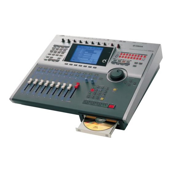
AW2816 PANEL LAYOUT Top panel Analog input/output section [GAIN] control [PEAK] indicators [PHONES] (headphones) control [MONITOR OUT] control WORK NAVIGATE section UNIT section [SETUP] key [SONG] key [UTILITY] key [FILE] key [MIDI] key [CD] key [PATCH] key [QUICK REC] (Quick Record) key... - Page 13 AW2816 FADER MODE section MIXING LAYER section INPUT [1-8] key [HOME] key RECORDER [1-8] key [AUX 5]/[AUX 6] keys RECORDER [9-16] key [AUX 1]~[AUX 4] keys [REMOTE] key Fader section [SEL] keys (1-8/STEREO/RTN 1/RTN 2) [ON] keys (1-8/STEREO/RTN 1/RTN 2)
- Page 14 AW2816 Display section Display [SHIFT] key [F1]-[F5] (Function 1-5) keys [CTRL] (Control) key Contrast Access indicator REC TRACK SELECT section RECORDER section [CUE] key [TRACK] key [METER] key [EDIT] key REC TRACK SELECT [1]–[16]/[ST] [UNDO] key [REDO] key [ALL SAFE] key...
- Page 15 AW2816 SCENE MEMORY section AUTOMATION section [STORE] key [AUTOMIX] key ] keys [SCENE] key [RECALL] key CURSOR/JOG&SHUTTLE section [JOG ON] key [DATA/JOG] dial [SHUTTLE] dial CURSOR [ ]/[ ]/[ ]/[ ] keys [ENTER] key...
- Page 16 AW2816 LOCATE section [NUM LOCATE] key [REPEAT] key MARK SEARCH [ ]/[ ] keys [A]/[B] keys [ROLL BACK] key ] key [MARK] key [RTZ] (Return to zero) key [AUTO PUNCH] key ] key LAST REC [IN]/[OUT] (Last recording in/out) key...
-
Page 17: Rear Panel
AW2816 Rear panel [PHANTOM +48V ON/OFF] switch DIGITAL STEREO OUT jack INPUT 1/2 (XLR) jacks SCSI connector INPUT 1/2 (TRS phone) jacks TO HOST connector FOOT SW jack INPUT 3–8 (TRS phone) jacks MIDI IN connector MIDI OUT/THRU connector INPUT 8 (Hi-Z) jack... -
Page 18: Circuit Board Layout
AW2816 CIRCUIT BOARD LAYOUT 〈 Bottom view 〉 Power Supply Unit SUB-MY CN504 CN503 MAIN SUB-FADER SEC A-A CN402 CN403 SUB-MY... - Page 19 AW2816 〈 Bottom view 〉 CN201 SUB-CPU CN305 CN303 CN301 CN307 CN302 CN306 CN401 CN301 CN601 CN101 CN702 CN703 MAIN CN502 CN101 CN103 CN104 CN102 SUB-FADER 〈 Bottom view 〉 SUB-INV CN502 CN501 CN503 CN101...
-
Page 20: Block Diagram
AW2816 BLOCK DIAGRAM... - Page 21 AW2816...
- Page 22 AW2816...
- Page 23 AW2816...
- Page 24 AW2816...
-
Page 25: Disassembly Procedure
AW2816 DISASSEMBLY PROCEDURE Bottom Cover (Time required: About 5 minutes) Remove the four (4) screws marked [720A] and turn over the HDD cover, and then pull out the HDD cable from the connector of the hard disk. The HDD cover can then be removed with the hard disk. - Page 26 AW2816 SUB-MY Circuit Board and Power Supply Unit (Time required: About 15 minutes each) Remove the bottom cover. (See procedure 1.) Remove the five (5) screws marked [700C]. The bottom chassis assembly can then be removed. (Fig.3) SUB-MY Circuit Board: Remove the two (2) screws marked [700D].
- Page 27 AW2816 MAIN and SUB-CPU Circuit Boards (Time required: About 25 minutes) Remove the eight (8) knobs marked [410] and the two (2) knobs marked [420] from the control panel side. (Fig.2) Remove the bottom cover. (See procedure 1.) Remove the bottom chassis assembly. (See procedure 3-2.)
- Page 28 AW2816 Remove the four (4) screws marked [700J]. The CD- RW holder can then be removed. (Fig.3) Remove the thirteen (13) screws marked [700K]. The sub chassis can then be removed. (Fig.7) Remove the four (4) screws marked [700L]. The LCD support can then be removed.
-
Page 29: Installing An Internal Hard Disk
AW2816 upside down. Please make sure that your work surface is spacious enough. • The AW2816 is shipped with four screws for attach- ing a 2.5 inch hard disk, and four screws for attach- ing a CD-RW drive, making a total of eight included screws of the same type. - Page 30 AW2816 From the bottom, unfasten the hard disk cover plate to which the internal 2.5 inch IDE hard disk will be attached. Hard disk cover plate The screws you remove will be used again to fasten the cover plate, so be careful not to lose them.
- Page 31 4, or identical screws. Using longer screws may damage the interior of the unit, or may cause elec- trical shock. • Do not turn on the power of the AW2816 until all options have been installed. • When you turn on the power of the AW2816 after installing a new hard disk, formatting of the hard disk will begin automatically.
-
Page 32: Installing A Cd-Rw Drive
CD- RW drive to set your CD-RW drive to function as a SLAVE unit. The AW2816 will not start up if the CD- RW is set to a mode other than SLAVE. -
Page 33: Installation Procedure
• Work surface • In order to install the CD-RW drive you will need to turn the AW2816 on its back. Make sure that you have a sufficiently broad work surface. • The AW2816 is shipped with four screws for attach- ing the 2.5 inch hard disk, and four screws for... - Page 34 Connect the flat cable ( ) and CD-RW drive power supply connector ( ) (from inside the AW2816) to the connectors of the CD-RW drive. Connect the flat cable first, and then the power supply connector. Power supply connector Flat cable...
- Page 35 AW2816 Align the fastening screw-holes on the bot- tom of the CD-RW drive with the screw- holes in the AW2816, and using a screw- driver and the included screws, fasten it in four locations. Re-attach the CD-RW drive cover and the bottom panel that you removed in step 4.
-
Page 36: Installing I/O Card
AW2816 INSTALLING I/O CARD Make sure that the power of the AW2816 is turned off. For safety’s sake, disconnect the power cable from the AC outlet. Always switch off the power for the main unit and all peripherals, unplug the power cord for the main unit... -
Page 37: Lsi Pin Description
AW2816 LSI PIN DESCRIPTION S1D13305F00B100 (XQ595A00) LCDC (LCD Controller) ..37 HD6437042AG12F (X0592A00) CPU ........38 HD6437042AF65F (XW647A00) CPU ........38 YSS910-S (XV988A00) DSP6 (Digital Signal Processor) ..39 YSS919-H (XZ693A00) DSP7 (Digital Signal Processor) ... 40 CI-DRC (XY629A00) Gate Array .......... 41 LR38791 (XY631A00) Gate Array ......... -
Page 38: Hd6437042Ag12F (X0592A00) Cpu
AW2816 HD6437042AG12F (X0592A00) CPU HD6437042AF65F (XW647A00) CPU MAIN: IC501,703 SUB-CPU: IC301 NAME FUNCTION NAME FUNCTION TIOC4/DACK0/PE14 MTU I/O / DMA acknowledge / Port E PE15 Port E Data bus Ground Ground Data bus Power supply Address bus Data bus Ground... -
Page 39: Yss910-S (Xv988A00) Dsp6 (Digital Signal Processor)
AW2816 YSS910-S (XV988A00) DSP6 (Digital Signal Processor) MAIN: IC404 NAME FUNCTION NAME FUNCTION Power supply (3.3 V) Ground Ground DB13 System master clock input (60 MHz or 30 MHz) DB14 System master clock output (High or 30 MHz) DB15 Power supply (5 V) -
Page 40: Yss919-H (Xz693A00) Dsp7 (Digital Signal Processor)
AW2816 YSS919-H (XZ693A00) DSP7 (Digital Signal Processor) MAIN: IC412 NAME FUNCTION NAME FUNCTION PLLEN PLL enable input (0: PLL unuse, 1: PLL use) SIO32 /TEST Test mode setting (0: TEST, 1: Normal) SIO33 AVss Analog ground SIO34 PLL filter SIO35... -
Page 41: Ci-Drc (Xy629A00) Gate Array
AW2816 CI-DRC (XY629A00) Gate Array MAIN: IC705 NAME FUNCTION NAME FUNCTION Ground Ground Not used Serial data input ... -
Page 42: Lr38791 (Xy631A00) Gate Array
AW2816 LR38791 (XY631A00) Gate Array SUB-CPU: IC302 NAME FUNCTION NAME FUNCTION FB17 Fader control LED8 LED control Ground Ground Power supply Power supply ... -
Page 43: Lr38792 (Xy630A00) Gate Array
AW2816 LR38792 (XY630A00) Gate Array MAIN: IC606 NAME FUNCTION NAME FUNCTION System address bus signal FS128 Clock Ground Ground Power supply Power supply XFS64 ... -
Page 44: S1R72104F00A100 (Xy625A00) Scsi Control
AW2816 S1R72104F00A100 (XY625A00) SCSI Control MAIN: IC719 NAME FUNCTION NAME FUNCTION Power supply +3.3V Power supply +3.3V EXCLK External clock input PD11 Ground OSCIN Oscillator input PD10 OSCOUT Oscillator output Port DMA data bus ... -
Page 45: Ak4528Vf (Xy624A00) Adc/Dac
AW2816 AK4528VF (XY624A00) ADC/DAC MAIN: IC301, 304, 307, 310 NAME FUNCTION NAME FUNCTION VCOM Common voltage output CKS0 Master clock select AINR+ Rch positive analog input CKS1 AINR- Rch negative analog input Digital audio interface select... - Page 46 AW2816 YM3436DK (XG948E00) DIR2 (Digital Format Interface Receiver) MAIN: IC408 NAME FUNCTION NAME FUNCTION DAUX Auxiliary input for audio data RSTN System reset input HDLT Asynchronous buffer operation flag VCO section power (+5 V) DOUT Audio data output CTLN VCO control input N...
-
Page 47: Ic Block Diagram
AW2816 IC BLOCK DIAGRAM HD74HC02FPEL (XL091A00) TC74VHC04FT (X0195A00) TC74VHC08FT (XV891A00) SN74HC02NSR (XW791A00) 74VHC04MTCX (X0292A00) Quad 2 Input AND Quad 2 Input NOR TC74HCT04AF-T1 (XI297A00) MAIN: IC721 HD74LS06FPEL (XH610A00) MAIN: IC421 Hex Inverter MAIN: IC515, 727 SUB-FADER: IC101, 102 TC74VHC11FT (X0197A00) - Page 48 AW2816 TC74VHCT245AFT (XT744A00) SN75179BPSR (XT619A00) TC74VHCT541AFT (XZ744A00) TC74VHC245FT (XU797A00) Line Driver 74VHCT541AMTCX (X0301A00) TC74HC245AF (XS720A00) Octal 3-State Buffer MAIN: IC413 MM74HC245ASJX (XW107A00) MAIN: IC507, 508, 513 Octal 3-State Bus Transceiver MAIN: IC401, 402, 506, 509-512, 607, 709, 710, 712, 716-718...
- Page 49 AW2816 NJM2068MD-T1 (XJ553A00) NJM2904M (XV190A00) BH9595FP-Y (XV617A00) NJM4556AMT1 (XQ138A00) Dual Operational Amplifier SCSI Terminator µPC4570G2 (XF291A00) MAIN: IC420 MAIN: IC720 Dual Operational Amplifier MAIN: IC101-108, 201-208, 209, 302, 303, 305, 306, 308, 309, 311, 312, Not to be used 313-315 +DC Voltage (N.C.)
-
Page 50: Circuit Boards
AW2816 CIRCUIT BOARDS SUB-MY Circuit Board (XZ717B0) ..........50 SUB-INV Circuit Board (XZ717B0) ..........51 MAIN Circuit Board (XZ715B0) ..........52/54 PN Circuit Board (XZ716B0) ............56 SUB-CPU Circuit Board (XZ717B0) ..........58 SUB-FADER Circuit Board (XZ717B0) ........60/61 Note: See parts list for details of circuit board component parts. - Page 51 AW2816 SUB-INV Circuit Board GREEN to LCD to MAIN -CN502 to LCD Pattern side Component side 3NA-V748650-2...
- Page 52 AW2816 MAIN Circuit Board to SUB-INV-CN503 CN503: to SUB-MY-CN402 to SUB-CPU-CN201 CN504: to SUB-MY-CN403 PHANTOM +48V ON/OFF MIC/LINE INPUT 3NA-V748630-2...
- Page 53 AW2816 IC with internal lithium battery (DS12887)REAL TIME CLOCK Part No.XV618A00 MAIN Circuit Board IC608 to CD-RW drive to 2.5" HDD drive to SUB-CPU-CN303 to Power supply unit-CN3 TO HOST SCSI PHONES HI-Z DIGITAL STEREO Component side 3NA-V748630-2...
- Page 54 AW2816 MAIN Circuit Board MONITOR OUT PHONES 3NA-V748630-3...
- Page 55 AW2816 MIC/LINE INPUT Pattern side 3NA-V748630-3...
- Page 56 AW2816 PN Circuit Board WORK NAVIGATE CD PLAY UNIT MIXER CH VIEW PAN/ EQ/ATT/ DYN/ ROUTING MIXER MIXER (FADER (FADER MODE) MODE) INPUT 1-8 RECORDER 1-8 RECORDER 9-16 MIXING LAYER SEL4/12 SEL1/9 SEL2/10 SEL3/11 SEL5/13 SEL6/14 SEL7/15 SEL8/16 SEL STEREO...
- Page 57 AW2816 REC TRACK SELECT RESET AUTOMATION RECORDER SCENE MEMORY SEL STEREO DATA/JOG/SHUTTLE CURSOR ON STEREO 8/MARK SEARCH > 7/MARK SEARCH < 9/MARK 5/LAST REC OUT to SUB-CPU -CN301 6/SET 4/LAST to SUB-CPU REC IN -CN305 3/ROLL BACK -/+/<< 0/RTZ Component side...
- Page 58 AW2816 SUB-CPU Circuit Board to SUB-FADER-CN104 to SUB-FADER-CN102 to SUB-FADER-CN103 to MAIN-CN301 STEREO OUT MONITOR OUT OMNI OUT UNBAL(-10dBV) BAL(+4dB) UNBAL(0dB) 3NA-V748650-2...
- Page 59 AW2816 to MAIN-CN601 to PN-CN102 to PN-CN101 OUT/THRU MTC OUT FOOT SW MIDI Component side Pattern side 3NA-V748650-2...
- Page 60 AW2816 SUB-FADER Circuit Board to SUB-CPU-CN306 FADER to SUB-CPU-CN302 to SUB-CPU-CN307 STEREO to Power supply unit -CN4 Component side 3NA-V748650-2...
- Page 61 AW2816 Pattern side 3NA-V748650-2...
-
Page 62: Test Program
AW2816 TEST PROGRAM 2) When the following title screen appears on the LCD, 1. Getting Ready release the keys. 1-1 Rear Panel (1) Insert the slot check card (TX800810) into an optional AW2816 I/O slot. (2) Connect an external hard disk drive unit to the SCSI Copy right ©... - Page 63 AW2816 3-4 Canceling a Test 4-2 LED Test (02 LED) (1) You can cancel a test that is currently running by “=== LED ===” is displayed on the LCD. (1) Test Content pressing the CANCEL key. 1) This test checks whether each control panel switch LED lights up correctly.
- Page 64 AW2816 2: CPU Interface (Data bus) ...NG 3) If the following NG messages appear: • • Checking R/W ...NG IC404 XXXX XXXX XXXX XXXX XXXX XXXX XXXX XXXX (“0” is displayed for the bits whose write and read 0XXX XXXX ...
- Page 65 AW2816 3) If the following NG messages appear: 4-8 Jog/Shuttle Function Test (08 JOG/SHUTTLE) 1: CPU Interface (Data bus) ...NG • “=== JOG/SHUTTLE ===” is displayed on the LCD. (1) Test Content IC412 XXXX XXXX XXXX XXXX XXXX XXXX XXXX XXXX 1) Checks jog/shuttle functions.
- Page 66 AW2816 2) If the following NG messages appear: 4-10 External SCSI Device Connection Test (10 SCSI) “=== SCSI ===” is displayed on the LCD. (1) Test Content 1) Checks connection and operation of the external SCSI device. (2) Judgment 1) If the external SCSI device is connected and operates correctly, OK will be displayed in the upper right corner of the screen.
- Page 67 AW2816 3) If one or both of the test results are NG and the (2) Judgment following message appears: 1) If all the test results are “OK” MIDI Tx/Rx→Signal error with TX0 (pin 15), RX0 • ENTER Press the key. The test menu will reappear (pin 14) of SIO4 (IC604) THRU SELECT→Signal error with Port E8 (pin 106)
- Page 68 AW2816 QUICK Press the key, and check that all the faders 4-15 Digital I/O Function Test (16 DIGITAL I/O) “=== DIGITAL I/O===” is displayed on the LCD. move near to the 0 (10) position. (1) Test Content 1) Checks whether the digital I/O (SPDIF format) signal...
- Page 69 AW2816 4-18 Real Time Clock Test (20 REAL TIME CLOCK) 5. Miscellaneous “=== REAL TIME CLOCK===” is displayed on the LCD. (1) Some switches have no LED, and they are indicated by a gray square in the illustration below. These...
- Page 70 AW2816...
- Page 71 AW2816...
- Page 72 AW2816...
- Page 73 AW2816...
- Page 74 AW2816...
- Page 75 AW2816...
- Page 76 AW2816...
- Page 77 AW2816...
-
Page 78: Display Message List
Undo (cancellation of an operation) is not possible. CD PLAY MODE NOW. Since the AW2816 is in CD Play mode, this operation is not possible. DIFFERENT TC FRAME TYPE MTC of a different frame type than the internal setting is being received. - Page 79 The Solo function is ready. Use the [SEL] keys to select the solo channel. SOLO READY. SOLO SLAVE. The Solo status cannot be changed when the AW2816 is functioning as a cascade slave. Press the Solo key on the master console. SONG NUMBER FULL.
-
Page 80: Popup Messages
Excessive amounts of data may have been received at the TO HOST TO HOST: RX BUFFER FULL! connector. The AW2816 may be attempting to transmit excessive amounts of TO HOST: TX BUFFER FULL! data from the TO HOST connector. Undo (cancellation of the previous operation) has been executed. - Page 81 A problem was found with the internal hard disk, and the AW2816 Illegal HDD! cannot start up correctly. If you want to format the internal hard disk for the AW2816, press the Format OK? [Y (Enter) /N (Any)] [ENTER] key. If you want to exchange the internal hard disk without formatting it for the AW2816, make sure that the access indicator is dark, and turn off the power.
- Page 82 AW2816...
- Page 83 AW2816...
- Page 84 AW2816...
- Page 85 AW2816...
-
Page 86: Midi Implementation Chart
AW2816 YAMAHA [PROFESSIONAL AUDIO WORKSTATION] Date: Mar 29, 2001 MIDI Implementation Chart Model: AW2816 Version: 1.0 Function... Transmitted Recognized Remarks Basic Default 1–16 1–16 Memorized Channel Changed 1–16 1–16 Memorized Default OMNI off/OMNI on Memorized Mode Messages Altered ************** Note 0–127... -
Page 87: Parts List
PROFESSIONAL AUDIO WORKSTATION PARTS LIST CONTENTS OVERALL ASSEMBLY ..........2 BOTTOM CHASSIS ASSEMBLY ..5 ELECTRICAL PARTS ..........6 Notes : DESTINATION ABBREVIATIONS A : Australian model M : South African model B : British model O : Chinese model C : Canadian model Q : South-east Asia model D : German model... - Page 88 AW2816 OVERALL ASSEMBLY T130 Top panel assembly T10a T10b Top cover assembly T10c T140 T10g T150 T100 T10f T10e T10d T110 T160 T170 T120 Bottom chassis assembly See page 5. Bottom cover assembly 320 660 720 710 300a 300b PWH screw...
- Page 89 AW2816 PART NO. DESCRIPTION REMARKS REF NO. RANK OVERALL ASSEMBLY AW2816 Overall Assembly (V748600) Overall Assembly U,C,V (V748610) Overall Assembly H,B,W (V748620) V 7 4 8 6 3 0 0 Circuit Board MAIN Circuit Board (V748650) AAX25110 Circuit Board SUB-CPU...
- Page 90 AW2816 PART NO. DESCRIPTION REMARKS REF NO. RANK V 6 1 9 0 6 0 0 AC Cord U,C,V V 6 1 9 0 7 0 0 AC Cord V 6 1 9 0 8 0 0 AC Cord BS 3P...
- Page 91 AW2816 BOTTOM CHASSIS ASSEMBLY PART NO. DESCRIPTION REMARKS REF NO. RANK BOTTOM CHASSIS ASSEMBLY AW2816 (V674350) V 6 7 4 3 8 0 0 Bottom Chassis V 5 4 1 4 3 0 0 Support, MY V 7 5 4 1 7 0 0...
- Page 92 AW2816 ELECTRICAL PARTS PART NO. DESCRIPTION REMARKS REF NO. RANK ELECTRICAL PARTS AW2816 V 7 4 8 6 3 0 0 Circuit Board MAIN (XZ715B0) V 7 4 8 6 4 0 0 Circuit Board (XZ716B0) AAX25110 Circuit Board SUB-CPU...
- Page 93 AW2816 PART NO. DESCRIPTION REMARKS REF NO. RANK C162 UF066470 Electrolytic Cap. (chip) 4.7 50V C163 UB245100 Monolithic Ceramic Cap. F 0.100 25V Z C164 UB214470 Monolithic Ceramic Cap. B 0.047 25V K C165 UB051100 Monolithic Ceramic Cap. SL 10P 50V D...
- Page 94 AW2816 PART NO. DESCRIPTION REMARKS REF NO. RANK C238 UB012220 Monolithic Ceramic Cap. B 220P 50V K C239 UF066470 Electrolytic Cap. (chip) 4.7 50V C240 UB245100 Monolithic Ceramic Cap. F 0.100 25V Z C241 UB214470 Monolithic Ceramic Cap. B 0.047 25V K...
- Page 95 AW2816 PART NO. DESCRIPTION REMARKS REF NO. RANK C316 UF037100 Electrolytic Cap. (chip) 10 16V -319 UF037100 Electrolytic Cap. (chip) 10 16V C320 UB012470 Monolithic Ceramic Cap. B 470P 50V K C321 VR325700 Mylar Capacitor (chip) 0.0033 16V J C322 UB012470 Monolithic Ceramic Cap.
- Page 96 AW2816 PART NO. DESCRIPTION REMARKS REF NO. RANK C396 UB051220 Monolithic Ceramic Cap. SL 22P 50V J C397 UB012470 Monolithic Ceramic Cap. B 470P 50V K C398 UB245100 Monolithic Ceramic Cap. F 0.100 25V Z C399 UB245100 Monolithic Ceramic Cap.
- Page 97 AW2816 PART NO. DESCRIPTION REMARKS REF NO. RANK -505 UB245100 Monolithic Ceramic Cap. F 0.100 25V Z C506 UF038100 Electrolytic Cap. (chip) 100 16V C551 UB245100 Monolithic Ceramic Cap. F 0.100 25V Z C552 UB245100 Monolithic Ceramic Cap. F 0.100 25V Z...
- Page 98 AW2816 PART NO. DESCRIPTION REMARKS REF NO. RANK CN301 VB390800 Connector Base Post PH 12P TE CN401 VB390500 Connector Base Post PH 9P TE CN502 VB390800 Connector Base Post PH 12P TE CN503 VQ048400 Connector, FFC 52045 35P TE CN504...
- Page 99 AW2816 PART NO. DESCRIPTION REMARKS REF NO. RANK IC503 XZ388A00 W24257S-70LL-EL10 IC504 X0613A00 MBM29F160BE-70TN FLASH ROM 16M IC505 XV932A00 MSM5118160D-60JSR1 DRAM 16M IC505 XV932B00 MSM5118160F-60J IC505 X0086A00 K4F151611D-JL6000 IC506 XU797A00 TC74VHC245FT BUFFER IC507...
- Page 100 AW2816 PART NO. DESCRIPTION REMARKS REF NO. RANK JK201 VT799400 Microphone Jack YKB21-5245 MIC/LINE INPUT 5-8 BAL -204 VT799400 Microphone Jack YKB21-5245 JK205 V 5 8 6 6 7 0 0 Phone Jack YKB21-5313 MIC/LINE INPUT 8 HI-Z JK301 VY961000...
- Page 101 AW2816 PART NO. DESCRIPTION REMARKS REF NO. RANK RD256470 Carbon Resistor (chip) 4.7K 0.1 J V I 1 9 7 0 0 0 Metal Film Resistor (chip) 6.8K 1/10 D V I 1 9 7 0 0 0 Metal Film Resistor (chip) 6.8K 1/10 D...
- Page 102 AW2816 PART NO. DESCRIPTION REMARKS REF NO. RANK R101 V I 1 9 6 6 0 0 Metal Film Resistor (chip) 4.7K 1/10 D R102 V I 1 9 8 5 0 0 Metal Film Resistor (chip) 30.0K 1/10 D...
- Page 103 AW2816 PART NO. DESCRIPTION REMARKS REF NO. RANK R178 V I 1 9 6 6 0 0 Metal Film Resistor (chip) 4.7K 1/10 D R179 V I 1 9 8 5 0 0 Metal Film Resistor (chip) 30.0K 1/10 D...
- Page 104 AW2816 PART NO. DESCRIPTION REMARKS REF NO. RANK R248 RD255330 Carbon Resistor (chip) 330.0 0.1 J R249 RD256820 Carbon Resistor (chip) 8.2K 0.1 J R250 V I 1 9 3 7 0 0 Metal Film Resistor (chip) 330.0 1/10 D...
- Page 105 AW2816 PART NO. DESCRIPTION REMARKS REF NO. RANK R333 V I 1 9 6 6 0 0 Metal Film Resistor (chip) 4.7K 1/10 D R334 V I 1 9 3 1 0 0 Metal Film Resistor (chip) 180.0 1/10 D...
- Page 106 AW2816 PART NO. DESCRIPTION REMARKS REF NO. RANK R403 RD254750 Carbon Resistor (chip) 75.0 0.1 J R404 V I 1 9 8 0 0 0 Metal Film Resistor (chip) 18.0K 1/10 D R405 V I 1 9 7 9 0 0 Metal Film Resistor (chip) 16.0K 1/10 D...
- Page 107 AW2816 PART NO. DESCRIPTION REMARKS REF NO. RANK R611 RD259100 Carbon Resistor (chip) 1.0M 0.1 J R612 RD256100 Carbon Resistor (chip) 1.0K 0.1 J R613 RD257100 Carbon Resistor (chip) 10.0K 0.1 J R616 RD250000 Carbon Resistor (chip) 0.0 0.0 J...
- Page 108 AW2816 PART NO. DESCRIPTION REMARKS REF NO. RANK TR107 VR936300 Transistor 2SA2SA1576AT106 TR108 VQ986700 Transistor 2SC2SC4081T106 TR109 I C 2 2 4 0 3 0 Transistor 2SC2240 GR,BL TR110 I C 2 2 4 0 3 0 Transistor 2SC2240 GR,BL...
- Page 109 AW2816 PART NO. DESCRIPTION REMARKS REF NO. RANK LD214 V 7 5 9 3 6 0 0 SLR-322YCT32 SEL 3/11 LD215 V 7 5 9 3 6 0 0 SLR-322YCT32 SEL 4/12 LD216 V 7 5 9 3 6 0 0...
- Page 110 AW2816 PART NO. DESCRIPTION REMARKS REF NO. RANK SW112 VV020300 Push Switch SKQNAA DYN/DLY <MIXER> SW113 VV020300 Push Switch SKQNAA AUX1 <MIXER(FADER MODE)> SW114 VV020300 Push Switch SKQNAA AUX2 <MIXER(FADER MODE)> SW115 VV020300 Push Switch SKQNAA AUX3 <MIXER(FADER MODE)> SW116...
- Page 111 AW2816 PART NO. DESCRIPTION REMARKS REF NO. RANK SW182 VV020300 Push Switch SKQNAA JOG ON SW183 VV020300 Push Switch SKQNAA <CURSOR> SW184 VV020300 Push Switch SKQNAA Down <CURSOR> SW185 VV020300 Push Switch SKQNAA Left <CURSOR> SW186 VV020300 Push Switch SKQNAA Right <CURSOR>...
- Page 112 AW2816 PART NO. DESCRIPTION REMARKS REF NO. RANK -206 UB245100 Monolithic Ceramic Cap. F 0.100 25V Z C301 UF038100 Electrolytic Cap. (chip) 100 16V C302 UF038100 Electrolytic Cap. (chip) 100 16V C303 UB245100 Monolithic Ceramic Cap. F 0.100 25V Z...
- Page 113 AW2816 PART NO. DESCRIPTION REMARKS REF NO. RANK L502 V 6 9 6 5 8 0 0 150uH LHL 08TB151K LD501 VQ559100 GL3EG44 R101 HV753220 Flame Proof C. Resistor 2.2 1/4 J R102 RD255100 Carbon Resistor (chip) 100.0 0.1 J...
- Page 114 AW2816 PART NO. DESCRIPTION REMARKS REF NO. RANK R503 RD257390 Carbon Resistor (chip) 39.0K 0.1 J R504 RD256120 Carbon Resistor (chip) 1.2K 0.1 J R505 RD156560 Carbon Resistor (chip) 5.6K 1/4 J R506 RD156560 Carbon Resistor (chip) 5.6K 1/4 J...
-
Page 115: Parts List
AW2816 AW2816 OVERALL CIRCUIT DIAGRAM 1/5 (MAIN1/3) MAIN (HA1) to SUB-MIDI - CN201 PHONES (AD/DA) PEAK PEAK PEAK PEAK OP AMP OP AMP OP AMP OP AMP OP AMP OP AMP OP AMP OP AMP OP AMP OP AMP REGULATOR +5V... -
Page 116: Parts List
AW2816 AW2816 OVERALL CIRCUIT DIAGRAM 2/5 (MAIN2/3) MAIN (DSP) DRAM 16M DRAM 16M DSP7 DSP6 SDRAM 16M MAIN2/3 M-10 MAIN3/3 G-2, I-8 MAIN2/3 M-10 MAIN3/3 G-2 MAIN1/3 N-7 REGULATOR REGULATOR REGULATOR +3.3V +3.3V not installed +2.5V not installed BUFFER MAIN3/3 O-1... -
Page 117: Parts List
AW2816 AW2816 OVERALL CIRCUIT DIAGRAM 3/5 (MAIN3/3) MAIN (GA) REGULATOR +5V INVERTER INVERTER LINE DRIVER TO HOST BUFFER LINE RECEIVER MAIN2/3 N-2 MAIN2/3 J-11 MULTIPLEXER GATE ARRAY (MAIN) MAIN2/3 J-2 GATE ARRAY REAL TIME CLOCK MAIN1/3 K-7 to SUB-CPU - CN303... - Page 118 AW2816 AW2816 OVERALL CIRCUIT DIAGRAM 4/5 (PN, SUB-CPU) SUB-CPU (SW) Transistor Array to SUB-FADER - CN102 SHUT PLUG-IN DOWN RECORDER Transistor Array CH VIEW to SUB-FADER - CN103 STEREO PLAY PAN/ ROUTING EFF1 GATE ARRAY Down EQ/ATT EFF2 /GRP installed...
-
Page 119: Parts List
AW2816 AW2816 OVERALL CIRCUIT DIAGRAM 5/5 (LCD, SUB-FADER, SUB-MY, SUB-INV) SUB-FADER MULTIPLEXER to SUB-CPU - CN302 to Power Suplly Unit - CN4 INVERTER INVERTER MOTOR MOTOR MOTOR MOTOR MOTOR DRIVER DRIVER DRIVER DRIVER DRIVER to SUB-CPU - CN306 MOTOR MOTOR... -
Page 120: Parts List
AW2816 AW2816 SOFTWARE BLOCK DIAGRAM STEREO MIC/LINE INPUT PHANTOM SELECTED INSERT RETURNS +48V METER METER INSERT INPUT 1(...8) LEVEL PEAK PREFADER LISTEN/ AFTER PAN 4BAND EQ NAMICS METER METER METER SOLO INPUT METER METER INSERT METER INSERT (EQ) LEVEL 4BAND EQ...