Sony ICF-SW07 Service Manual
Hide thumbs
Also See for ICF-SW07:
- Operating instructions manual (252 pages) ,
- Service manual (63 pages) ,
- Specifications (2 pages)

Related Manuals for Sony ICF-SW07


Summary of Contents for Sony ICF-SW07
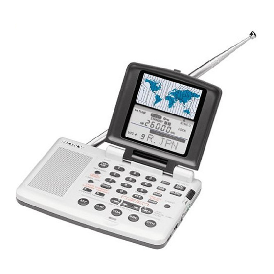
- Page 1 ICF-SW07 AN-LP2 SERVICE MANUAL US Model Canadian Model Ver 1.0 1999.02 AEP Model E Model Tourist Model Antenna Controller Antenna mdule AN-LP2 ICF-SW07 SPECIFICATIONS FM STEREO/SW/MW/LW PLL SYNTHESIZED RECEIVER MICROFILM...
-
Page 2: Table Of Contents
DIAGRAMMES SCHÉMATIQUES ET LA LISTE DES PIÈCES SONT CRITIQUES POUR LA SÉCURITÉ DE FONCTIONNEMENT. NE REMPLACER CES COMPOSANTS QUE PAR DES PIÈCES SONY DONT LES NUMÉROS SONT DONNÉS DANS CE MANUEL OU DANS LES SUPPLÉMENTS PUBLIÉS PAR SONY. – 2 –... -
Page 3: Service Note
• Only the most recent version is supplied for replacing the Sony ROM. • A new Sony ROM is issued every year in October and the part No. suffix is also changed. • A new updated Sony ROM is issued every year so is not usually kept in stock. -
Page 4: General
SECTION 2 This section is extracted from GENERAL instruction manual. LOCATION AND FUNCTION OF CONTROLS – 4 –... - Page 5 – 5 –...
- Page 6 – 6 –...
- Page 7 – 7 –...
- Page 8 – 8 –...
- Page 9 – 9 –...
- Page 10 – 10 –...
- Page 11 – 11 –...
- Page 12 – 12 –...
- Page 13 – 13 –...
- Page 14 – 14 –...
- Page 15 – 15 –...
- Page 16 – 16 –...
- Page 17 – 17 –...
- Page 18 – 18 –...
- Page 19 – 19 –...
- Page 20 – 20 –...
- Page 21 – 21 –...
- Page 22 – 22 –...
- Page 23 – 23 –...
- Page 24 – 24 –...
-
Page 25: Disassembly
SECTION 3 DISASSEMBLY The equipment can be removed using the following procedure. <RADIO SECTION> Cabinet (Lower) ASSY Main board Chassis ASSY Cabinet ASSY Key board Microcomputer board <ANTENNA CONTROLLER SECTION> Cabinet (Front), Reel ASSY Cabinet (Rear), Reel board, Control board Note : Follow the disassembly procedure in the numerical order given. -
Page 26: Chassis Assy
3-2. CHASSIS ASSY 2 Screw (1.4x4) Main board Chassis ASSY 4 Remove solder Black Flexible board Brown Cabinet ASSY Caution A portion of the chassis and cabinet ASSY are joined by adhesive sheet so use caution during removal. 3-3. MAIN BOARD Terminal (+), Battery 5 Flexible board (Key board:CN701) -
Page 27: Key Board
3-4. KEY BOARD 2 Screw (1.4x3) Key board Sheet 1 Cut the sheet 3 Push this place, and Claw release a claw 6 Flexible board Chassis 4 Claws 3-5. MICROCOMPUTER BOARD Lid (front) Microcomputer board Frame (lid) !¡ 7 Claws 9 Screws (1.4x4) Lid (rear) ASSY... -
Page 28: Cabinet (Front), Reel Assy
<ANTENNA CONTROLLER SECTION> 3-6. CABINET (FRONT), REEL ASSY Reel ASSY Cabinet (front) Cabinet (rear) ASSY Reel board Lid, Battery case 3 Screw, Step Surface of contacts 2 Screws (M 1.7) 2 Screws (M 1.7) Note on instalation : Apply grease (J-2502-028-1) to the surface of contacts on the reel board. -
Page 29: Electrical Adjustments
SECTION 4 ELECTRICAL ADJUSTMENTS AM SECTION 1 st IF Adjustment 0dB=1µV BAND : AM VOLUME control : as required 2nd LOCAL Adjustment Setup : BAND : AM VOLUME control : as required Put the lead-wire AM RF SSG Connection Points : antenna close to the set. - Page 30 SW FREQUENCY Adjustment Procedure : BAND : AM 1. Align the set with the frequency of the AM RF signal generator VOLUME control : as required shown on the table below. Connection Points : 2. Align RV401 - RV412 for each band meter band until the high- est reading is obtained on the level meter.
- Page 31 FM SECTION FM TRACKING Adjustment Note : This adjustment should be performed after the remove Rod Antenna (ANT102). FM FREQUENCY COVERAGE Adjustment This adjustment should be performed after the FM FRE- BAND : FM QUENCY COVERAGE ADJUSTMENT. VOLUME control : as required Connection Points : Digital BAND : FM...
- Page 32 FM STEREO Adjustment SD Adjustment BAND : FM BAND : FM ST • MONO switch : ST VOLUME control : as required VOLUME control : as required Connection Points : Connection Points : FM RF SSG servicing tool DC5V TP(ANT) 2.4k Ω...
- Page 33 FM 100MHz Adjustment MICROCOMPUTER SECTION BAND : FM VOLUME control : as required 4MHz SYSTEM CLOCK Adjustment Connection Points : BAND : AM servicing tool VOLUME control : as required Connection Points : DC5V 2.4k Ω servicing tool frequency 0.01 µ F DC5V 2.4k Ω...
-
Page 34: Diagrams
SECTION 5 DIAGRAMS 5-1. EXPLANATION OF IC TERMINALS IC402 µPD17072GB-556-1A7 (PLL SYNTHESIZER CONTROL) Pin No. Pin name Description ROD/BAR ROD/BAR antenna select output. “H” : BAR, “L” : ROD AM/FM AM/FM select output. “H” : AM, “L” : FM ENV/PSN ENV/PSN select output. - Page 35 IC501 µPD753017AGK-717-BE9 (MAIN SYSTEM CONTROL, LCD DRIVE) Pin No. Pin name Description 1 – 12 S12 – 23 LCD segment signal output. 13 – 16 ––––– – Not used (OPEN). XTAL-CTL Level shift control output for system clock. BEEP-CTL Beep signal control ouptut. IF-POWER IF B+ ON/OFF control output.
- Page 36 – Not used (OPEN). 68 – 80 S0 – S11 LCD segment signal output. Circuit Boards Location MICROCOMPUTER board ROM board REEL board MAIN board KEY board CONTROL board ANTENNA board ICF-SW07 ANTENNA CONTROLLER SW LOOP ANTENNA – 36 –...
-
Page 37: Block Diagrams
ICF-SW07 5-2. BLOCK DIAGRAMS • Signal path. : FM : SW L : MW/LW – 37 – – 38 – – 39 – – 40 –... -
Page 38: Schematic Diagram (Main Section)
ICF-SW07 5-4. SCHEMATIC DIAGRAM (MAIN SECTION) Refer to page 63 for IC Block Diagrams. Waveforms (MAIN Section) Note: • All capacitors are in µF unless otherwise noted. pF: µµF 50 WV or less are not indicated except for electrolytics and tantalums. -
Page 39: Schematic Diagram (Key Section)
ICF-SW07 5-6. SCHEMATIC DIAGRAM (KEY SECTION) 5-5. PRINTED WIRING BOARDS (KEY SECTION) Semiconductor Location Ref. No. Location Note: IC801 G-12 • All capacitors are in µF unless otherwise noted. pF: µµF 50 WV or less are not indicated except for electrolytics... -
Page 40: Printed Wiring Boards (Microcomputer Section)
ICF-SW07 5-8. SCHEMATIC DIAGRAM (MICROCOMPUTER SECTION) 5-7. PRINTED WIRING BOARDS (MICROCOMPUTER SECTION) Semiconductor Note: Location • X : parts extracted from the component side. • : Through hole. Ref. No. Location • b : Pattern of the rear side. D501 •... -
Page 41: Schematic Diagram (Antenna Section)
ICF-SW07 5-9. PRINTED WIRING BOARDS (ANTENNA SECTION) 5-10. SCHEMATIC DIAGRAM (ANTENNA SECTION) Semiconductor Location Ref. No. Location D901 B-11 D902 IC901 C-10 Q901 Q902 B-10 Q903 B-10 • Voltages are dc with respect to ground under no-signal Note: (detuned) conditions. - Page 42 IC Block Diagrams (MAIN Section) IC403 LA5002M IC201 CXA1376AM WAKE REF. VOLTAGE AM FE FM FE ERROR CONTROL AM IF SYNC DE ENV DET FM DEM FM LIM AM VCO METER FM IF IC302 CXA1622M IC301 LA3335M GND1 P-GND1 OUT1 LAMP SYNC DECODER...
-
Page 43: Exploded Views
SECTION 6 EXPLODED VIEWS NOTE : • -XX, -X mean standardized parts, so they • The mechanical parts with no reference may have some difference from the original number in the exploded views are not one. supplied • Items marked “ * ”are not stocked since they •... -
Page 44: Chassis Section
6-2. CHASSIS SECTION SP301 ANT101 Ref. No. Part No. Description Remark Ref. No. Part No. Description Remark * 51 A-3683-027-A MAIN BOARD, COMPLETE * 61 A-3638-687-A CONNECTOR ASSY 1-672-549-11 FLEXIBLE BOARD 3-384-797-01 SCREW 3-031-529-01 TERMINAL (-), BATTERY 3-031-494-01 CHASSIS 3-031-491-01 BUTTON (10 KEY) 3-031-520-01 KNOB(TONE) X-3376-861-1 CABINET ASSY 3-031-518-01 TERMINAL (+), BATTERY... -
Page 45: Antenna Controller Section
6-3. ANTENNA CONTROLLER SECTION P902 Ref. No. Part No. Description Remark Ref. No. Part No. Description Remark 3-015-956-01 LID, BATTERY CASE 3-015-949-01 CABINET (REAR) 3-907-747-01 SPRING (+/-.B), BATTERY * 108 1-666-723-11 REEL BOARD 3-895-517-11 SCREW (2), TAPPING, STEP * 109 A-3683-030-A CONTROL BOARD, COMPLETE 3-363-895-01 SCREW (M1.7) 3-030-407-01 CABINET (FRONT) -
Page 46: Sw Loop Antenna Section
6-4. SW LOOP ANTENNA SECTION Ref. No. Part No. Description Remark Ref. No. Part No. Description Remark 3-910-063-01 SCREW (1.7X10) 3-015-953-11 CASE (UPPER) 3-015-954-01 CASE (LOWER) 3-018-979-01 CLIP (SUCKER) * 153 A-3683-029-A ANTENNA BOARD, COMPLETE X-3374-227-2 ANTENNA ASSY – 67 –... -
Page 47: Electrical Parts List
SECTION 7 ANTENNA CONTROL ELECTRICAL PARTS LIST NOTE : • Due to standardization, replacements in the • SEMICONDUCTORS In each case, u : µ , for example : The components identified by mark ! parts list may be different from the parts uA.. - Page 48 CONTROL MAIN Ref. No. Part No. Description Remark Ref. No. Part No. Description Remark < TRANSISTOR > R731 1-218-953-11 RES,CHIP 1/16W Q901 8-729-402-32 TRANSISTOR 2SD1819A-R R732 1-218-953-11 RES,CHIP 1/16W Q902 8-729-800-71 TRANSISTOR 2SB815B7-TB R733 1-218-953-11 RES,CHIP 1/16W Q903 8-729-402-32 TRANSISTOR 2SD1819A-R R734 1-218-953-11 RES,CHIP 1/16W...
- Page 49 MAIN Ref. No. Part No. Description Remark Ref. No. Part No. Description Remark C105 1-107-813-11 TANTAL. CHIP 10uF 6.3V C163 1-107-811-11 TANTAL. CHIP 47uF C201 1-162-970-11 CERAMIC CHIP 0.01uF C106 1-162-925-11 CERAMIC CHIP 68PF C202 1-162-979-11 CERAMIC CHIP 2700PF C107 1-162-913-11 CERAMIC CHIP 0.5PF C203...
- Page 50 MAIN Ref. No. Part No. Description Remark Ref. No. Part No. Description Remark C326 1-115-156-11 CERAMIC CHIP C439 1-107-813-11 TANTAL. CHIP 10uF 6.3V C440 1-164-005-11 CERAMIC CHIP 0.47uF C327 1-115-156-11 CERAMIC CHIP C441 1-164-005-11 CERAMIC CHIP 0.47uF C328 1-107-813-11 TANTAL. CHIP 10uF 6.3V C442...
- Page 51 MAIN Ref. No. Part No. Description Remark Ref. No. Part No. Description Remark D202 8-719-002-81 DIODE 1T363 Q102 8-729-037-89 TRANSISTOR 2SC4627J-C(TX).SO D203 8-719-002-81 DIODE 1T363 Q103 8-729-123-86 TRANSISTOR 2SK238-K16 D301 8-719-421-67 DIODE MA132WK Q104 8-729-037-92 TRANSISTOR 2SD2216J-R(TX).SO D401 8-719-046-91 DIODE MA2S111 Q105 8-729-037-92 TRANSISTOR 2SD2216J-R(TX).SO D402...
- Page 52 MAIN Ref. No. Part No. Description Remark Ref. No. Part No. Description Remark Q401 8-729-220-93 TRANSISTOR 2SK209-G R111 1-218-937-11 RES,CHIP 1/16W R112 1-218-973-11 RES,CHIP 1/16W Q402 8-729-220-93 TRANSISTOR 2SK209-G R113 1-218-937-11 RES,CHIP 1/16W Q403 8-729-037-92 TRANSISTOR 2SD2216J-R(TX).SO R114 1-216-839-11 METAL CHIP 1/16W Q404 8-729-037-71 TRANSISTOR UN9210J-(TX).SO...
- Page 53 MAIN Ref. No. Part No. Description Remark Ref. No. Part No. Description Remark R201 1-216-826-11 METAL CHIP 2.7K 1/16W R404 1-216-833-11 METAL CHIP 1/16W R202 1-216-851-11 METAL CHIP 330K 1/16W R405 1-216-833-11 METAL CHIP 1/16W R406 1-216-833-11 METAL CHIP 1/16W R203 1-216-837-11 METAL CHIP 1/16W...
- Page 54 MAIN MICROCOMPUTER Ref. No. Part No. Description Remark Ref. No. Part No. Description Remark R462 1-216-851-11 METAL CHIP 330K 1/16W RV410 1-241-482-11 RES, ADJ, CERMET 220K(16mb) R463 1-216-851-11 METAL CHIP 330K 1/16W RV411 1-241-482-11 RES, ADJ, CERMET 220K(41mb) RV412 1-241-482-11 RES, ADJ, CERMET 220K(13mb) R464 1-216-850-11 METAL CHIP...
- Page 55 MICROCOMPUTER Ref. No. Part No. Description Remark Ref. No. Part No. Description Remark C515 1-162-970-11 CERAMIC CHIP 0.01uF < CONNECTOR > C516 1-162-970-11 CERAMIC CHIP 0.01uF CN502 1-785-566-21 HOUSING, FPC CONNECTOR(ZIF)35P C517 1-162-927-11 CERAMIC CHIP 100PF C518 1-162-927-11 CERAMIC CHIP 100PF <...
- Page 56 MICROCOMPUTER REEL ROM Ref. No. Part No. Description Remark Ref. No. Part No. Description Remark R510 1-216-825-11 METAL CHIP 2.2K 1/16W R566 1-216-825-11 METAL CHIP 2.2K 1/16W R567 1-216-825-11 METAL CHIP 2.2K 1/16W R511 1-216-825-11 METAL CHIP 2.2K 1/16W R568 1-216-797-11 METAL CHIP 1/16W R512...
- Page 57 ICF-SW07 Ref. No. Part No. Description Remark 1-694-491-11 CONDUCTIVE BOARD,CONNECTION(A) 1-672-549-11 FLEXIBLE BOARD ANT101 1-501-657-22 FERRITE-ROD ANTENNA (MW/LW) ANT102 1-501-658-11 ANTENNA, TELESCOPIC (FM/SW) EL501 1-803-372-11 ELEMENT, EL INDICATION(LCD BACK LIGHT) LCD501 1-803-371-11 PANEL, LIQUID CRYSTAL DISPLAY P902 1-790-234-11 CODE (WITH PLUG)
- Page 58 This file has been downloaded from: www.electronica.ro Service Manuals, Schematic Diagram, Repair...