Advertisement
Quick Links
Download this manual
See also:
User Manual
INTRODUCTION
The Motorola M6800 Microcomputer System of standard LSI (Large Scale
Integration) devices permits the systems designer to configure and connect a
total system with a minimum amount of time and effort. The MC6800
Microprocessing Unit (MPU) forms the nucleus of the system. LSI modules
available which may be used to configure a total system in conjunction with
the MC6800 MPU, include: 1) MC6810 Random Access Memory (RAM); 2) MC6830 Read
Only Memory (ROM); 3) MC6820 Peripheral Interface Adapter (PIA), and 4)
MC6850 Asynchronous Communications Interface Adapter (ACIA).
The MPU communicates with the rest of the system via a 16 bit
address bus and an 8 bit data bus. The 16 bit address bus provides the MPU
the capability of addressing up to 64K. The 8 bit data bus is bi-directional
in that data is transferred both into the MPU or out of the MPU over the same
bus. A read/write (R/W) line is provided to allow the MPU to control the
direction of data transfer.. Since the same bus is used for both data into
the MPU or out of the MPU, a separate 8 line bus is saved.
Other features of the M6800 system include a single +5 volt supply,
operation at clock rates from 100 kilohertz to 1 megahertz, plus hardware and
software interrupt capability.
MPU-1
Advertisement

Related Manuals for Motorola M6800


Summary of Contents for Motorola M6800
- Page 1 Since the same bus is used for both data into the MPU or out of the MPU, a separate 8 line bus is saved. Other features of the M6800 system include a single +5 volt supply, operation at clock rates from 100 kilohertz to 1 megahertz, plus hardware and software interrupt capability.
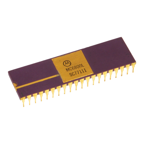
- Page 2 Microprocessing Unit (MC6800) The nucleus of the M6800 Microcomputer Family is the microprocessing unit (MPU). The MPU is enclosed in a 40 pin package as shown below: Features included in the MPU are: Two accumulators (ACCA and ACCB) One index register (X)
- Page 3 One condition code register (CC) 72 instructions Five addressing modes System clock range of 100 kilohertz to 1 megahertz Program interrupt capability Accumulators The MPU contains 2 accumulators designated ACCA and ACCB. Each accumulator is 8 bits (one byte) long and is used to hold operands and data from the arithmetic logic unit.
- Page 4 INC – Increment LDA - Load accumulator LSR - Logical shift right NEA - Negate ORA - Inclusive OR PSH - Push data onto stack PUL - Pull data from stack ROL - Rotate left ROR - Rotate right RTI - Return from interrupt SBA - Subtract accumulators...
- Page 5 CPX - Compare index register DEX - Decrement index register INX - Increment index register LDX - Load index register RTI - Return from interrupt STX - Store index register SWI - Software interrupt TSX - Transfer stack pointer to index register TXS - Transfer index register to stack pointer WAI - Wait for interrupt Program Counter...
- Page 6 The condition code register is an 8 bit register. Each individual bit may get set or get cleared from execution of an instruction. To see how each instruction effects the condition code register, refer to the M6800 programming manual. The primary use of this register is execution of the conditional branch instruction.
- Page 7 Carry-Borrow: For addition, the carry-borrow condition code (C) in the zero bit position, represents a carry. This bit gets set (C=1) to indicate a carry, and is reset (C=0) if there is no carry. For subtraction, the C bit is set (C=1) to indicate a borrow and is reset (C=0) to indicate there was no borrow.
-
Page 8: Interrupt Request(Irq)
1. READ/WRITE (R/W): This output line is used to signal all devices external to the MPU that the MPU is in a read state (R/W = High) or a write state (R/W = Low). The normal standby state of this line when no external devices are being accessed is a high state. -
Page 9: Non-Maskable Interrupt(Nmi)
Counter, Accumulators, and Condition Code Register are stored away on the stack. Next the MPU will respond to the interrupt request by setting the interrupt mask bit high so that no further interrupts may occur. At the end of the cycle, a 16-bit address will be loaded that points to a vectoring address which is located in memory locations n-6 and n-7 where n is the highest ROM address. - Page 10 Request signal, the processor will complete the current instruction that is being executed before it recognizes the NMI signal. The interrupt mask bit in the Condition Code Register has no effect on NMI. The Index Register, Program Counter, Accumulators, and Condition Code Register are stored away on the stack.
- Page 11 available. This will occur if the GO/HALT line is in the Halt (low) mode or the 14PU is in a "Wait" state as the result of some instruction, such as the WAI instruction. THREE-STATE CONTROL: (TSC) This input causes all of the address lines and the Read/Write line to go into the off or high impedance state.
- Page 12 Microprocessor Instruction Set -- Alphabetic Sequence Add Accumulators Add with Carry Logical And Arithmetic Shift Left Arithmetic Shift Right Branch if Carry Clear Branch if Carry Set Branch if Equal to Zero Branch if Greater or Equal Zero Branch if Greater than Zero Branch if Higher Bit Test Branch if Less or Equal...
- Page 13 What happens when the MPU gets a hardware interrupt? After it has been determined that the interrupt is not non-maskable, the MPU checks the status of the mask bit (bit 4 of the condition code register). If the mask bit is set, the main program continues until a CLI (clears bit 4 of condition code register) instruction is executed, after which time the MPU will honor an interrupt by going to the stack pointer (SP) register and fetch an address...
- Page 14 MPU-14...
- Page 15 SUMMARY OF MPU OPERATION The MPU requires a two phase symmetrical, TTL compatible, nonoverlapping clock. During the first phase of the clock (Ø l high) an address will be placed on the address bus by the MPU. During the second phase of the clock (Ø...
-
Page 16: Reset Sequence
RESET SEQUENCE 1. While HALT is high, RESET goes low for at least eight cycles of Ø l , Ø 2 during which all internal registers are cleared and interrupt bit (I) in CC is set. 2. Data at FFFE loads into PCH. 3. - Page 17 IRQ SEQUENCE 1. If bit "I" in condition code register is not set (I = 0) and IRQ goes low for at least one Ø 2 cycle, the IRQ sequence will be entered. 2. After completion of the current instruction, internal registers PC, X, A, B and CC will be stored in RAM at the address indicated by the stack pointer in descending locations (7 bytes in all).
- Page 18 NMI SEQUENCE 1. If NMI goes low for at least one Ø 2 cycle, the MPU will wait for completion of current instruction. 2. The internal registers PC, X, A, B and CC will then be stored in RAM at the address indicated by the stack pointer in descending locations (7 bytes in all).
-
Page 19: Swi Instruction
SWI INSTRUCTION Contents of the MPU registers PC, 1X, ACCA, ACCB and CC are stored in RAM at the address indicated by the stack pointer in descending location (7 bytes in all). The IRQ mask (bit I = 1) is set. Data at FFFA gets loaded into PCH. - Page 20 Everyone is quite familiar with the base 10 number system i.e. 0, 1, 2, 3, 4, 5, 6, 7, 8, & 9, since this is the system we all use day to day. Let us review a typical number, say 2743, and see what it really means. The least significant digit (LSD) is 3 and the most significant digit (MSD) is 2.
- Page 21 101111 2 = lx2 0 + 1x2 1 + lx2 2 + lx2 3 + 0x2 4 + 1x2 5 = 1x1 + 1x2 = 47 10 In general, converting from a number in any base to a number in base 10 is accomplished as follows: (A 0 B 0 + A 1 B 1 + A 2 B 2 + A 3 B 3 + A 4 B 4 -- -- -- -- A n B n ) where B is the base of the number system and A is the particular digit in the...
- Page 22 First lets prove that 75 8 & 111101 2 are really equal to 61 10 . 75 8 = 5x8 0 + 7x8 1 = 5x1 + 7x8 = 5 + 56 = 61 10 111101 2 = 1x2 0 + 0x2 1 + 1x2 2 + 1x2 3 + 1x2 4 + 1x2 5 = 1x1 = 61 10 Notice that if we take the base 8 number of 75 and convert each...
- Page 23 Therefore 75 8 - 111101 which is the same pattern of 1's & 0's as we got from converting from base 10 to base 2. What this really says that it is easier to convert any base 10 number to base 8 by continuous division, and then convert each digit of the base 8 number to base 2.
- Page 24 Digital computers are designed to use binary numbers in their working registers. The working registers vary in number of bits depending on the manufacturer. The Motorola M6800 micro-processor utilizes, in general, 8 bit words (or registers). This leads to another number base, not yet mentioned, of hexadecimal.
- Page 25 147 8 = 7x8 0 + 4x8 1 + 1x8 2 = 7x1 + 4x8 + 1x64 + 32 + 64 = 103 10 67 16 = 7x16 0 + 6x16 1 = 7x1 + 6x16 + 96 = 103 10 As you probably have wondered by now, how do we represent these hex (base 16) numbers above 9? Here is the base 16 number compared with its equivalent base 10 number.
- Page 26 To convert any base 10 number to hex (base 16) you may convert it to base 8 first, then represent the base 8 number with its binary representation. By taking the binary representation of the number and grouping the bits from right to left in groups of four which are then represented in hex per the above table.
- Page 27 825 10 to octal 825 10 to binary 825 10 = 1471 8 = 1x8 0 + 7x8 1 + 4x8 2 + 1x8 3 = 1x1 + 7x8 + 4x64 + 1x512 + 56 + 256 = 825 10 1471 8 1100111001 2 + 512...
- Page 28 825 10 = 1100111001 2 = 1x2 0 +Ox2 1 +0x2 2 +lx2 3 +1x2 4 +1x2 5 +0x2 6 +0x2 7 = lxl +0x2 +0x4 = 825 10 Or taking 147l 8 and representing each digit by its binary representation, we get 1=001, 4=100, 7=111 &...
- Page 29 Conversion Chart Decimal Octal Hexadecimal Binary 0000 0000 0000 0001 0000 0010 0000 0011 0000 0100 0000 0101 0000 0110 0000 0111 0000 1000 0000 1001 0000 1010 0000 1011 0000 1100 0000 1101 0000 1110 0000 1111 0001 0000 0001 0001 0001 0010 0001 0011...