Harman Kardon AVR 235 Service Manual
Hide thumbs
Also See for AVR 235:
- Service manual (122 pages) ,
- Owner's manual (57 pages) ,
- Quick start manual (4 pages)

Related Manuals for Harman Kardon AVR 235


Summary of Contents for Harman Kardon AVR 235
- Page 1 ® Power for the Digital Revolution ® AVR 235 AUDIO/VIDEO RECEIVER SERVICE MANUAL...
-
Page 2: Technical Specifications
Height measurement includes feet and chassis. All features and specifications are subject to change without notice. Harman Kardon is a registered trademark, and Power for the digital revolution is a trademark, of Harman International Industries, Inc. is a trademark of Harman International Industries, Inc. -
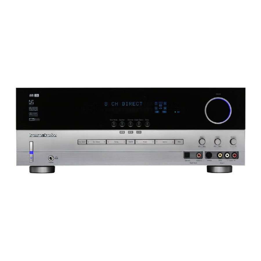
Page 3: Front Panel Controls
Front Panel Controls ˜ ¯ Û ˆ & ı Ù Ú Ó Ô Ò Main Power Switch Tuner Band Selector Ô Video 4 input jacks System Power Control Set Button Bass Control Ò Power Indicator Preset Stations Selector Balance Control Headphone Jack Speaker/Channel Input Indicator... - Page 4 Front Panel Controls 7 Selector Buttons: When you are establishing $ Speaker/Channel Input Indicators: These Bass Control: Turn this control to modify the the AVR’s configuration settings, use these buttons indicators are multipurpose, indicating either the low frequency output of the left/right channels by to select from the choices available, as shown in speaker type selected for each channel or the as much as ±10dB.
-
Page 5: Rear Panel Connections
Rear Panel Connections AM Antenna DVD Video Inputs Surround Back Speaker Outputs FM Antenna Front Speaker Outputs Video 1 Video Outputs Tape Inputs Center Speaker Outputs Video 1 Video Inputs Tape Outputs Surround Speaker Outputs Video 2 Video Outputs Subwoofer Output Switched AC Accessory Outlet Video 3 Video Inputs DVD Audio Inputs... - Page 6 Connect this jack to 12 for more information on speaker polarity.) to the PLAY/OUT audio jacks on any audio or the “IR IN” jack on Harman Kardon or other F Surround Speaker Outputs: Connect video source. compatible equipment.
-
Page 7: Surround Mode Chart
8-Channel Direct Inputs 9 so that the sound field is enhanced by adding back surround channels. Logic 7 Cinema Exclusive to Harman Kardon for AV receivers, Logic 7 is an advanced mode that extracts the Delay time not adjustable Logic 7 Music... -
Page 8: Troubleshooting Guide
Power switch 2 is red due to possible short and speaker ends • Amplifier is in protection mode • Contact your local Harman Kardon service depot due to internal problems No sound from surround or • Incorrect surround mode •... - Page 9 AVR235/230 EXPLODED VIEW 38-2 40-1 40-4 40-3 40-2 39-1 40-5 37-9 38-1 37-7 DESCRIPTION PARTS NO. Q,ty CAP,VOLUME CGX1A338MBC22 HOLDER,VOLUME CMH1A214 INDICATOR,VOLUME CGL1A222 WINDOW,FIP CGU1A366Y KNOB,ROTARY CBN1A174MBC22 FILTER,FIP CMZ1A088 BDAGE,HARMAN/KARDON KGB1A111X PANEL,FRONT CGW1A366RDWH43 BRACKET,SIDE CMD2A443 KNOB,FUNCTION CBT1A905MBYC22 KNOB,SET CBT1A904MBZC22 KNOB,DELAY CBT1A819K128 KNOB,POWER CBT1A903MMZC22...
- Page 10 AVR235/230 1. Instruction manual ass'y - Accessories 2. Package Drawing ACCESSORY-1 REMOCON TRANSMITTER ASS'Y POLY BAG AM LOOP ANTENNA ASS'Y BATTERY ASS'Y SNOW PAD (L) SNOW PAD (R) FM 1 POLE ANT STAPLE POLY BAG COVER ASS'Y BOX ,OUT CARTON BOOKLET,INFORMATION MANUAL INSTRUCTION MANUAL SETUP GUIDE...
- Page 11 Front PCB assy Ref# Component Description 1 Description 2 COP11745F FRONT PCB ASS'Y C701 HCBS1H390JT CAP , CERAMIC 39PF 50V J C702 HCBS1H390JT CAP , CERAMIC 39PF 50V J C703 HCBS1H821KBT CAP , CERAMIC 820PF 50V K C704 HCEA1VH100T CAP , ELECT 10UF 35V C705 HCBS1H102KBT CAP , CERAMIC...
- Page 12 Front PCB assy Ref# Component Description 1 Description 2 C798 KCFE1J332JBT CAP , FILM 0.0033UF 63V J C799 KCFE1J183JBT CAP , FILM 0.018UF 63V J C800 KCFE1J183JBT CAP , FILM 0.018UF 63V J C805 HCBS1H223ZFT CAP , CERAMIC 0.022UF 50V Z C806 HCBS1H223ZFT CAP , CERAMIC 0.022UF 50V Z...
- Page 13 Front PCB assy Ref# Component Description 1 Description 2 D774 HVD1SS133MT DIODE 1SS133T-77 D778 KVD1N4003ST DIODE 1N4003 D779 HVD1SS133MT DIODE 1SS133T-77 D780 HVD1SS133MT DIODE 1SS133T-77 D781 HVD1SS133MT DIODE 1SS133T-77 D782 KVD1N4003ST DIODE 1N4003 D783 HVD1SS133MT DIODE 1SS133T-77 D784 HVD1SS133MT DIODE 1SS133T-77 D785 HVD1SS133MT DIODE...
- Page 14 Front PCB assy Ref# Component Description 1 Description 2 R728 CRD20TJ101T RES , CARBON 100 OHM 1/5W J R730 CRD20TJ112T RES,CABON 1.1K OHM 1/5W R731 CRD20TJ223T RES , CARBON 22K OHM 1/5W J R732 CRD20TJ202T RES , CARBON 2K OHM 1/5W R733 CRD20TJ272T RES , CARBON 2.7K OHM 1/5W J...
- Page 15 Front PCB assy Ref# Component Description 1 Description 2 R830 CRD20TJ184T RES , CARBON 180K OHM 1/5W R831 CRD20TJ562T RES , CARBON 5.6K OHM 1/5W J R832 CRD20TJ562T RES , CARBON 5.6K OHM 1/5W J R833 CRD20TJ102T RES , CARBON 1K OHM 1/5W J R834 CRD20TJ102T RES , CARBON...
- Page 16 Front PCB assy Ref# Component Description 1 Description 2 R899 CRD20TJ104T RES , CARBON 100K OHM 1/5W J R900 CRD20TJ104T RES , CARBON 100K OHM 1/5W J R901 CRD20TJ152T RES , CARBON 1.5K OHM 1/5W J R902 CRD20TJ152T RES , CARBON 1.5K OHM 1/5W J R903 CRD20TJ102T RES , CARBON...
- Page 17 Front PCB assy Ref# Component Description 1 Description 2 BN90 CWB2B902090EN WIRE ASS'Y BN94 KJP13GB99ZM CONNECTOR MOLEX35237-1310 1 BN95 KJP08GB99ZM CONNECTOR , HOUSING MOLEX35237-0810 1 CN10 KJP04GB46ZM WAFER MOLEX 53015 CN11 KJP15GA98ZM WAFER MOLEX35336-1510 1 CN12 KJP15GA98ZM WAFER MOLEX35336-1510 1 CN15 CJP06GA19ZY WAFER, STRAIGHT, 6PIN CN16 KJP08GB46ZM...
- Page 18 Front PCB assy Ref# Component Description 1 Description 2 CTB3+10G SCREW CTB3+16GFZ SCREW CTWS3+10G SCREW KHR301 CLAMPER CB72 CWC1B2A32A250B CABLE , CARD MAIN PCB Assy Ref# Component Description 1 Description 2 COP11746F MAIN PCB ASS'Y C501 HCEA1VH100T CAP , ELECT 10UF 35V C502 HCEA1VH100T CAP , ELECT...
- Page 19 MAIN PCB Assy Ref# Component Description 1 Description 2 C803 CCCT1H330JC CAP , CERAMIC 33PF 50V JC C804 CCCT1H330JC CAP , CERAMIC 33PF 50V JC C805 CCCT1H120JC CAP , CERAMIC 12PF 50V JC C806 CCCT1H120JC CAP , CERAMIC 12PF 50V JC C811 HCEA1CH101T CAP , ELECT 100UF 16V...
- Page 20 MAIN PCB Assy Ref# Component Description 1 Description 2 D581 HVD1SS133MT DIODE 1SS133T-77 D582 HVD1SS133MT DIODE 1SS133T-77 D583 HVD1SS133MT DIODE 1SS133T-77 D584 HVD1SS133MT DIODE 1SS133T-77 D585 HVD1SS133MT DIODE 1SS133T-77 D601 HVD1SS133MT DIODE 1SS133T-77 D801 HVD1SS133MT DIODE 1SS133T-77 D802 HVD1SS133MT DIODE 1SS133T-77 D803 HVD1SS133MT DIODE...
- Page 21 MAIN PCB Assy Ref# Component Description 1 Description 2 Q562 HVTKTC3200GRT KTC3200GR Q563 HVTKTC3200GRT KTC3200GR Q564 HVTKTC3200GRT KTC3200GR Q565 HVTKTC3200GRT KTC3200GR Q601 HVTKTA1268GRT KTA1268GR Q602 HVTKTA1268GRT KTA1268GR Q603 HVTKTA1268GRT KTA1268GR Q604 HVTKTA1268GRT KTA1268GR Q605 HVTKTA1268GRT KTA1268GR Q681 KVTKSC2785YT KSC2785Y Q682 KVTKSC2785YT KSC2785Y Q683 KVTKSC2785YT KSC2785Y...
- Page 22 MAIN PCB Assy Ref# Component Description 1 Description 2 Q970 HVTKTC2874BT T.R , MUTE KTC2874B Q971 HVTKTC2874BT T.R , MUTE KTC2874B Q972 HVTKTC2874BT T.R , MUTE KTC2874B Q973 HVTKTC2874BT T.R , MUTE KTC2874B Q991 HVTKRC107MT KRC107M Q992 HVTKRA107MT KRA107M R501 CRD20TJ433T RES , CARBON 43K OHM 1/5W J R502 CRD20TJ433T...
- Page 23 MAIN PCB Assy Ref# Component Description 1 Description 2 R568 CRD20TJ561T RES , CARBON 560 OHM 1/5W J R569 CRD20TJ561T RES , CARBON 560 OHM 1/5W J R570 CRD20TJ561T RES , CARBON 560 OHM 1/5W J R571 CRD20TJ561T RES , CARBON 560 OHM 1/5W J R572 CRD20TJ561T RES , CARBON...
- Page 24 MAIN PCB Assy Ref# Component Description 1 Description 2 R649 KRD25FJ3R3T RES , CARBON 3.3 OHM 1/4W J R650 KRD25FJ3R3T RES , CARBON 3.3 OHM 1/4W J R651 KRD25FJ3R3T RES , CARBON 3.3 OHM 1/4W J R652 KRD25FJ3R3T RES , CARBON 3.3 OHM 1/4W J R653 KRD25FJ3R3T RES , CARBON...
- Page 25 MAIN PCB Assy Ref# Component Description 1 Description 2 R726 CRD20TJ104T RES , CARBON 100K OHM 1/5W J R727 CRD20TJ104T RES , CARBON 100K OHM 1/5W J R728 CRD20TJ104T RES , CARBON 100K OHM 1/5W J R771 CRD20TJ750T RES , CARBON 75 OHM 1/5W J R772 CRD20TJ750T RES , CARBON...
- Page 26 MAIN PCB Assy Ref# Component Description 1 Description 2 R853 CRD20TJ152T RES , CARBON 1.5K OHM 1/5W J R854 CRD20TJ152T RES , CARBON 1.5K OHM 1/5W J R855 CRD20TJ152T RES , CARBON 1.5K OHM 1/5W J R856 CRD20TJ221T RES , CARBON 220 OHM 1/5W J R857 CRD20TJ221T RES , CARBON...
- Page 27 MAIN PCB Assy Ref# Component Description 1 Description 2 R952 CRD20TJ223T RES , CARBON 22K OHM 1/5W J R953 CRD20TJ223T RES , CARBON 22K OHM 1/5W J R954 CRD20TJ223T RES , CARBON 22K OHM 1/5W J R955 CRD20TJ203T RES , CARBON 20K OHM 1/5W J R956 CRD20TJ394T RES , CARBON...
- Page 28 MAIN PCB Assy Ref# Component Description 1 Description 2 Q804 BVT2SB1560-OKM T.R , POWER 2SB1560 Q805 BVT2SD2390-OKM T.R , POWER 2SD2390 Q807 BVT2SB1560-OKM T.R , POWER 2SB1560 CTW3+8J SCREW BN19 CWB3FE03250UP WIRE ASS'Y BN20 CWB3FB43280UP WIRE ASS'Y BN79 CWZAVR230BN79 WIRE ASS'Y (SHIELD) BN81 CWB1C902050EN WIRE ASS'Y BN82 CWB1C902050EN...
- Page 29 MAIN PCB Assy Ref# Component Description 1 Description 2 JK97 CJJ4P041W JACK IN/OUT JK98 CJJ4P042W JACK IN/OUT JW90 CWEE212120VV WIRE ASS'Y JW91 CWE8212180VV WIRE ASS'Y JW99 CWE8202150AA WIRE ASS'Y L501 CLEY0R5KAK COIL , SPEAKER 0.5UH L502 CLEY0R5KAK COIL , SPEAKER 0.5UH L503 CLEY0R5KAK...
- Page 30 BIAS PCB ASSY Ref# Component Description 1 Description 2 R877 CRD20TJ331T RES , CARBON 330 OHM 1/5W J R878 CRD20TJ331T RES , CARBON 330 OHM 1/5W J R879 CRD20TJ331T RES , CARBON 330 OHM 1/5W J R880 CRD20TJ331T RES , CARBON 330 OHM 1/5W J R882 CRD20TJ122T RES , CARBON...
- Page 31 DSP / Input PCB ASSY Ref# Component Description 1 Description 2 C253 HCUS1H181JA CAP , CHIP 1068 SIZE C254 HCUS1H471JA CAP , CHIP 1068 SIZE C255 HCUS1H223ZF CAP , CHIP 1068 SIZE C256 HCUS1H223ZF CAP , CHIP 1068 SIZE C270 HCUS1H181JA CAP , CHIP 1068 SIZE C271 HCUS1H471JA...
- Page 32 DSP / Input PCB ASSY Ref# Component Description 1 Description 2 C427 HCUS1H151JA CAP , CHIP , 150PF JA 1608 SIZE C428 HCUS1H151JA CAP , CHIP , 150PF JA 1608 SIZE C429 HCUS1H151JA CAP , CHIP , 150PF JA 1608 SIZE C430 HCUS1H151JA CAP , CHIP , 150PF JA 1608 SIZE...
- Page 33 DSP / Input PCB ASSY Ref# Component Description 1 Description 2 IC31 HVINJM2068MDTE1 I.C , OP AMP NJM2068MD-TE1 IC32 HVINJM2068MDTE1 I.C , OP AMP NJM2068MD-TE1 IC33 HVINJM2068MDTE1 I.C , OP AMP NJM2068MD-TE1 IC34 HVINJM2068MDTE1 I.C , OP AMP NJM2068MD-TE1 IC35 HVINJM2068MDTE1 I.C , OP AMP NJM2068MD-TE1...
- Page 34 DSP / Input PCB ASSY Ref# Component Description 1 Description 2 R219 CRJ10DJ471T RES , CHIP 1608 SIZE R220 CRJ10DJ471T RES , CHIP 1608 SIZE R221 CRJ10DJ471T RES , CHIP 1608 SIZE R222 CRJ10DJ471T RES , CHIP 1608 SIZE R223 CRJ10DJ471T RES , CHIP 1608 SIZE R224 CRJ10DJ272T...
- Page 35 DSP / Input PCB ASSY Ref# Component Description 1 Description 2 R291 CRJ10DJ472T RES , CHIP 1608 SIZE R292 CRJ10DJ472T RES , CHIP 1608 SIZE R293 CRJ10DJ472T RES , CHIP 1608 SIZE R301 CRJ10DJ332T RES , CHIP 1608 SIZE R302 CRJ10DJ332T RES , CHIP 1608 SIZE R303 CRJ10DJ332T...
- Page 36 DSP / Input PCB ASSY Ref# Component Description 1 Description 2 R368 CRJ10DJ104T RES , CHIP 1608 SIZE R371 CRJ10DJ332T RES , CHIP 1608 SIZE R372 CRJ10DJ332T RES , CHIP 1608 SIZE R373 CRJ10DJ332T RES , CHIP 1608 SIZE R374 CRJ10DJ332T RES , CHIP 1608 SIZE R375 CRJ10DJ332T...
- Page 37 DSP / Input PCB ASSY Ref# Component Description 1 Description 2 R456 CRJ10DJ184T RES , CHIP 1608 SIZE R457 CRJ10DJ184T RES , CHIP 1608 SIZE R458 CRJ10DJ184T RES , CHIP 1608 SIZE R459 CRJ10DJ184T RES , CHIP 1608 SIZE R460 CRJ10DJ184T RES , CHIP 1608 SIZE R471 CRJ10DJ272T...
- Page 38 DSP / Input PCB ASSY Ref# Component Description 1 Description 2 R768 CRJ10DJ152T RES , CHIP 1608 SIZE R769 CRJ10DJ103T RES , CHIP 1608 SIZE R770 CRJ10DJ103T RES , CHIP 1608 SIZE R771 CRJ10DJ330T RES , CHIP 1608 SIZE R772 CRJ10DJ330T RES , CHIP 1608 SIZE R773 CRJ10DJ103T...
- Page 39 DSP / Input PCB ASSY Ref# Component Description 1 Description 2 C237 CCEA1CH101T CAP , ELECT 100UF 16V C238 CCEA1CH101T CAP , ELECT 100UF 16V C239 CCEA1VH100T CAP , ELECT 10UF 35V C240 CCEA1VH100T CAP , ELECT 10UF 35V C251 CCEA1CH101T CAP , ELECT 100UF 16V C252 CCEA1CH101T...
- Page 40 DSP / Input PCB ASSY Ref# Component Description 1 Description 2 C455 CCEA1VH100T CAP , ELECT 10UF 35V C456 CCEA1VH100T CAP , ELECT 10UF 35V C457 CCEA1VH100T CAP , ELECT 10UF 35V C458 CCEA1VH100T CAP , ELECT 10UF 35V C459 CCEA1VH100T CAP , ELECT 10UF 35V C460 CCEA1VH100T...
- Page 41 DSP / Input PCB ASSY Ref# Component Description 1 Description 2 JK15 CJJ4R037W JACK , BOARD JW21 CWE7202090AA WIRE ASS'Y J103 C3A206 WIRE , COPPER SN95/PB5 , 0.6 0,018 J104 C3A206 WIRE , COPPER SN95/PB5 , 0.6 0,018 L701 KLZ9H001Z BEAD , CORE L702 KLZ9H001Z...
- Page 42 VIDEO PCB ASSY Ref# Component Description 1 Description 2 C404 CCKT1H101KB CAP , CERAMIC 100PF 50V KB C405 HCEA1VH100T CAP , ELECT 10UF 35V C406 HCEA1VH100T CAP , ELECT 10UF 35V C407 CCKT1H101KB CAP , CERAMIC 100PF 50V KB C408 CCEA1VH100T CAP , ELECT 10UF 35V C409 CCKT1H101KB...
- Page 43 VIDEO PCB ASSY Ref# Component Description 1 Description 2 C462 HCEA1CH101T CAP , ELECT 100UF 16V C463 HCBS1H473ZFT CAP , CERAMIC 0.047UF 50V Z C498 HCBS1H151KBT CAP , CERAMIC 150PF 50V K C499 HCBS1H151KBT CAP , CERAMIC 150PF 50V K C501 HCBS1H270JT CAP , CERAMIC 27PF 50V...
- Page 44 VIDEO PCB ASSY Ref# Component Description 1 Description 2 Q403 HVTKRA107MT KRA107M Q404 HVTKRC107MT KRC107M Q405 HVTKSA733CYT Q406 HVTKRA107MT KRA107M Q407 HVTKRC107MT KRC107M Q408 HVTKRC107MT KRC107M Q409 HVTKRA104MT KRA104M Q410 HVTKTD1302T KTD1302 Q411 HVTKTD1302T KTD1302 Q412 HVTKRA104MT KRA104M Q501 KVTKSC2785YT KSC2785Y Q502 KVTKSA1175YT KSA1175Y...
- Page 45 VIDEO PCB ASSY Ref# Component Description 1 Description 2 R445 CRD20TJ1R0T RES , CARBON 1 OHM 1/5W J R446 CRD20TJ102T RES , CARBON 1K OHM 1/5W J R447 CRD20TJ750T RES , CARBON 75 OHM 1/5W J R448 CRD20TJ1R8T RES , CARBON 1.8 OHM 1/5W J R449 CRD20TJ102T RES , CARBON...
- Page 46 VIDEO PCB ASSY Ref# Component Description 1 Description 2 R569 CRD20TJ223T RES , CARBON 22K OHM 1/5W J X501 HOX17734E220C CRYSTAL 17.734MHZ X502 HOX14318E220C CRYSTAL 14.318MHZ IC48 CVIL7805CPNA I.C ASS'Y CMY1A218 HEAT SINK(TR) AVR130/230/330 CTB3+8J SCREW HVIL7805CP I.C, REGULATOR IC49 CVIL7905CPNA I.C ASS'Y CMY1A218...
- Page 47 power supply (drawing CUP11747-5) Ref# Component Description 1 Description 2 SW91 KST1A010Z SW , TACT D101 HVDMTZJ15BT DIODE , ZENER 15V 1/2W D102 HVDMTZJ27BT DIODE , ZENER 27V 1/2W D104 KVD1N4003ST DIODE 1N4003 D105 KVD1N4003ST DIODE 1N4003 D106 KVD1N4003ST DIODE 1N4003 D107 KVD1N4003ST DIODE...
- Page 48 power supply (drawing CUP11747-4) Ref# Component Description 1 Description 2 F903 KJCFC5S HOLDER , FUSE F904 KJCFC5S HOLDER , FUSE F905 KJCFC5S HOLDER , FUSE F906 KJCFC5S HOLDER , FUSE F907 KJCFC5S HOLDER , FUSE T901 CLT5W011ZE TRANS , POWER 230V Low voltage regulator PCB Ref# Component...
- Page 49 TRANSISTOR, REGULATOR IC BLOCK DIAGRAM TO-92L TO-92M TO-92 TO-220 1. Emitter 1. Emitter 1. Emitter 1. GND 2. Collector 2. Collector 2. Collector 2. INPUT 3. Base 3. Base 3. Base 3. OUTPUT 1 2 3 12 3 KTA1024Y KSC2316Y KTC2874B KSC2785Y KTD1302T...
- Page 50 TC9162AF (FUNCTION/INPUT : IC28) TC9162AF (FUNCTION/INPUT : IC30) BLOCK DIAGRAM BLOCK DIAGRAM L-COM L-COM R-COM R-COM L-COM L-COM R-COM R-COM L-COM L-COM R-COM R-COM L-COM L-COM R-COM R-COM DATA DATA SHIFT REGISTER SHIFT REGISTER...
- Page 51 TC9164AF (FUNCTION/INPUT) : IC23 BLOCK DIAGRAM L-COM R-COM L-COM R-COM L-COM R-COM DATA SHIFT REGISTER TC9163AF (FUNCTION/INPUT) : IC21,24 BLOCK DIAGRAM L-COM R-COM L-COM R-COM L-COM R-COM DATA SHIFT REGISTER...
- Page 52 U-COM BLOCK DIAGRAM , PIN ASSIGNMENT & PIN DESCRIPTIONS S3C84BB/F84BB BLOCK DIAGRAM (IC74) P0.0-P0.7 P1.0-P1.7 Port 0 Port 1 OSC/RESETB Port 2 P2.0-P2.7 RESETB I/O Port and Interrupt Control 8-Bit Basic Timer P2.7/TAOUT 8-Bit P2.6/TACAP Port 3 P3.0-P3.7 Timer P2.5/TACK /CounterA,B P2.4/TBOUT SAM88RC CPU...
- Page 53 S3C84BB/F84BB PRODUCT OVERVIEW PIN ASSIGNMENT (IC74) P2.5/TACK P8.2 P2.4/TBPWM P8.3 P2.3/DAOUT P8.4/INT8 P2.2/SCK P8.5/INT9 P2.1/SI P6.0 P2.0/SO P6.1 P5.7 P6.2 P5.6/SDAT P6.3 P5.5/SCLK S3C84BB/F84BB P6.4 VDD1 VDD2 VSS1 VSS2 (80-TQFP-1212) XOUT P6.5 P6.6 TEST P6.7 P5.4 P7.0/ADC0 P5.3/RxD0 P7.1/ADC1 RESETB P7.2/ADC2 P5.2/TxD0 P7.3/ADC3...
- Page 54 PRODUCT OVERVIEW S3C84BB/F84BB PIN DESCRIPTIONS (IC74) Table 1-1. S3C84BB/F84BB Pin Descriptions (80-QFP) Circuit Share Name Type Description Type Number Pins P0.0 - P0.7 I/O Bit programmable port; input or output mode 80-73 PG0-PG7 selected by software; input or push-pull output. Software assignable pull-up.
- Page 55 S3C84BB/F84BB PRODUCT OVERVIEW Table 1-1. S3C84BB/F84BB Pin Descriptions (80-QFP) (Continued) Circuit Share Name Type Description Type Number Pins P4.0 - P4.7 I/O Bit programmable port; input or output mode 38-31 INT0– selected by software; input or push-pull output. INT7 Software assignable pull-up. P4.0-P4.7 can alternately be used as inputs for external interrupts INT0-INT7, respectively (with noise filters and interrupt controller)
- Page 56 PRODUCT OVERVIEW S3C84BB/F84BB Table 1-1. S3C84BB/F84BB Pin Descriptions (80-QFP) (Continued) Circuit Share Name Type Description Type Number Pins AD0 - AD7 Analog input pins for A/D converter module. 48–45 P7.0–P7.7 Alternatively used as general-purpose digital 42–39 input port 7. AVREF, AVSS A/D converter reference voltage and ground 43, 44 RxD0, RxD1...
- Page 57 IC86...
- Page 58 NJM2581 DUAL SUPPLY WIDE BAND 3ch VIDEO AMPLIFIER GENERAL DESCRIPTION PACKAGE OUTLINE The NJM2581 is a dual supply voltage wide band 3ch video amplifier. It is suitable for Y, Pb, and Pr signal because frequency range is 50MHz. The NJM2581 is suitable for Set Top Box, AV amplifier, and other high quality AV systems.
- Page 59 BLOCK DIAGAM (NJM2296M ) : IC41, 42, 43 Vin1 Vin2 Vout1 6.2dB dirver Vin3 6.2dB Vout2 dirver Vin4 6.2dB Vout3 dirver Vin5...
- Page 60 NJM2068M (OP-AMP)
- Page 61 U-COM IC PIN ASSIGNMENT & DESCRIPTIONS PIN ASSIGNMENT (IC72) (TOP VIEW) P20/A16 P21/A17 P22/A18 P57/CLK P23/A19 P24/A20/PPG0 P56/RDY P25/A21/PPG1 P55/HAK P26/A22/PPG2 P54/HRQ P27/A23/PPG3 P53/WRH P30/A00/AIN0 P52/WRL P31/A01/BIN0 P51/RD P50/ALE P32/A02/ZIN0 PA3/OUT3 P33/A03/AIN1 PA2/OUT2 P34/A04/BIN1 PA1/OUT1 P35/A05/ZIN1 PA0/OUT0 P36/A06 P97/IN1 P37/A07 P96/IN0 P40/A08/SIN2 P95/PPG5...
- Page 62 MB90482 PIN DESCRIPTIONS (IC72) Pin No. Circuit Pin name Function type LQFP* QFP* Oscillator pin Oscillator pin 32 kHz oscillator pin 32 kHz oscillator pin Reset input pin This is a general purpose I/O port. A setting in the pull-up resistance setting register (RDR0) can be used to apply pull-up P00 to P07 resistance (RD00-RD07 = “1”) .
- Page 63 MB90482 Pin No. Circuit Pin name Function type LQFP* QFP* This is a general purpose I/O port. In non-multiplex mode, this pin functions as an external address pin. (CMOS/H) AIN0 8/16-bit up/down timer input pin (channel 0) . This is a general purpose I/O port. In non-multplex mode, this pin functions as an external address pin.
- Page 64 MB90482 Pin No. Circuit Pin name Function type LQFP* QFP* P43, P44 This is a general purpose I/O port. In non-multiplex mode, this pin functions as an external (CMOS) A11, A12 address pin. This is a general purpose I/O port. In non-multiplex mode, this pin functions as an external (CMOS) address pin.
- Page 65 MB90482 Pin No. Circuit Pin name Function type LQFP* QFP* This is a general purpose I/O port. In external bus mode, when the RYE bit in the EPCR register is set to “1”, this pin functions as the RDY pin. (CMOS) In external bus mode, this pin functions as the external ready (RDY) input pin.
- Page 66 MB90482 (Continued) Pin No. Circuit Pin name Function type LQFP* QFP* This is a general purpose I/O port. SIN1 Simple serial I/O data input pin. (CMOS/H) Chip select 0. This is a general purpose I/O port. SOT1 Simple serial I/O data output pin. (CMOS) Chip select 1.
- Page 67 O.S.D IC (74763M) Pin Functions (IC51) Pin No. Symbol Function Description Ground Ground connection Xtal Connection for the crystal and capacitor used to form the crystal oscillator that generates Crystal oscillator connection the internal synchronization signal. The oscillator can be selected with a command switch. Xtal OUT1 Horizontal synchronization...
- Page 68 LC74763, 74763M Pin Assignment Top view Serial Data Input Timing No. 5039-4/19...
- Page 69 LC74763, 74763M System Block Diagram No. 5039-5/19...
- Page 70 HCF4053B FUNCTION DIAGRAM & PIN DESCRIPTION INPUT EQUIVALENT CIRCUIT PIN DESCRIPTION (IC44,45,51,80,89) PIN No SYMBOL NAME AND FUNCTION 11, 10, 9 A, B, C Binary Control Inputs Inhibit Inputs 12, 13, 2, 1, ax,ay,bx,by,cx,cy Input/ IN/OUT 5, 3 Output OUT/IN ax or ay OUT/IN bx or by...
- Page 73 AUDIO DSP (CS493263 - CLG : IC75) PIN No. Pin Name Function 1,12,23 +VD1 Digital Power supply. Normally +2.5v 2,13,24 DGND Digital Ground AUD3 SPDIF transmitter output/Digital audio output(N.C) Host write strobe pin(connected to GND with an external resistor) Host parallel output enable pin(pulled up with an external resistor) CS_DA SPI Serial data input pin CS_CK...
-
Page 74: Top View
PIN ASSIGNMENT.(CS493263) DGND1 MCLK AUDATA3, XMT958 SCLK WR,DS,EMWR,GPIO10 LRCLK RD,R/W,EMOE,GPIO11 AUDATA0 A1,SCDIN AUDATA1 A0,SCCLK AUDATA2 6 5 4 3 2 1 44 43 42 41 40 DATA7,EMAD7,GPIO7 DATA6,EMAD6,GPIO6 DATA5,EMAD5,GPIO5 RESET DATA4,EMAD4,GPIO4 AGND CS493XXX-CLG 44-pin PLCC Top View DGND2 FILT1 DATA3,EMAD3,GPIO3 FILT2 DATA2,EMAD2,GPIO2 CLKSEL... - Page 75 AKM CONFIDENTIAL ASAHI KASEI [AK5381] IC 76 = Preliminary = AK5381 24Bit 96kHz ∆Σ ADC GENERAL DESCRIPTION The AK5381 is a stereo A/D Converter with wide sampling rate of 4kHz ∼ 96kHz and is suitable for High-end audio system. The AK5381 achieves high accuracy and low cost by using Enhanced dual bit ∆Σ...
- Page 76 AKM CONFIDENTIAL ASAHI KASEI [AK5381] Ordering Guide −40 ∼ +85°C AK5381VT 16pin TSSOP (0.65mm pitch) AKD5381 Evaluation Board for AK5381 Pin Layout AINR CKS0 AINL CKS2 CKS1 VCOM Top View AGND SCLK MCLK LRCK DGND SDTO Compatibility with AK5380 AK5380 AK5381 Master Mode Not Available...
- Page 77 AKM CONFIDENTIAL ASAHI KASEI [AK5381] PIN / FUNCTION No. Pin Name Function AINR Rch Analog Input Pin AINL Lch Analog Input Pin CKS1 Mode Select 1 Pin Common Voltage Output Pin, VA/2 VCOM Bias voltage of ADC input. AGND Analog Ground Pin Analog Power Supply Pin, 4.5 ∼...
- Page 78 ASAHI KASEI [AK4358] AKM CONFIDENTIAL AK4358 = Target Spec = 192kHz 24-Bit 8ch DAC with DSD Input GENERAL DESCRIPTION The AK4358 is eight channels 24bit DAC corresponding to digital audio system. Using AKM's advanced multi bit architecture for its modulator the AK4358 delivers a wide dynamic range while preserving linearity for improved THD+N performance.
- Page 79 ASAHI KASEI [AK4358] AKM CONFIDENTIAL n Ordering Guide AK4358VQ -40 ∼ +85°C 48LQFP AKD4358 Evaluation Board for AK4358 n Pin Layout (To be determined) AVSS LOUT1- AVDD LOUT1+ DZF3 VREFH ROUT4+ DZF2 AK4358VQ DZF1 ROUT4- DIF0 CAD0 DSDR3 Top View DSDL3 DSDR2 BICK...
- Page 80 ASAHI KASEI [AK4358] AKM CONFIDENTIAL n Compatibility with AK4357 1. Function & Performance Functions AK4357 AK4358 # of channels 106dB 114B 48kHz/96kHz TDM Not available Available Not available Available DSDM control Pin/Register Register Input channel of DZF pin Fixed Programmable 2.
- Page 81 ASAHI KASEI [AK4358] AKM CONFIDENTIAL IC 74 PIN/FUNCTION (TBD) Pin Name Function LOUT1- DAC1 Lch Negative Analog Output Pin LOUT1+ DAC1 Lch Positive Analog Output Pin DZF1 Zero Input Detect 1 Pin DZF2 Zero Input Detect 2 Pin DZF3 Zero Input Detect 3 Pin CAD0 Chip Address 0 Pin Power-Down Mode Pin...
- Page 82 DIR IC PIN ASSIGNMENT & BLOCK DIAGRAM PIN ASSIGNMENT (TOP VIEW) : IC73 INT0 IPS0/RX4 OCKS0/CSN/CAD0 AVSS OCKS1/CCLK/SCL DIF0/RX5 TEST2 CM1/CDTI/SDA AK4114VQ CM0/CDTO/CAD1 DIF1/RX6 AVSS DIF2/RX7 Top View IPS1/IIC DAUX P/SN XTL0 MCKO2 BICK XTL1 SDTO...
-
Page 83: Block Diagram
BLOCK DIAGRAM AVSS AVDD X'tal Clock Oscillator 8 to 3 Recovery Clock MCKO1 Generator MCKO2 Input Selector LRCK DAIF Audio BICK Decoder SDTO DAUX DVDD Error & Q-subcode CCLK DVSS AC-3/MPEG µP I/F STATUS CDTO buffer TVDD Detect Detect CDTI B,C,U,VOUT INT0 INT1... - Page 84 DIR IC PIN FUNCTION (AK4114VQ) : IC73 PIN/FUNCTION Pin Name Function IPS0 Input Channel Select 0 Pin in Parallel Mode Receiver Channel 4 Pin in Serial Mode (Internal biased pin) No Connect NC(AVSS) No internal bonding. This pin should be connected to AVSS. DIF0 Audio Data Interface Format 0 Pin in Parallel Mode Receiver Channel 5 Pin in Serial Mode (Internal biased pin)
- Page 85 PIN/FUNCTION (Continued) Pin Name Function Power-Down Mode Pin When “L”, the AK4114 is powered-down and reset. Master Clock Operation Mode 0 Pin in Parallel Mode CDTO Control Data Output Pin in Serial Mode, IIC= “L”. CAD1 Chip Address 1 Pin in Serial Mode, IIC= “H”. Master Clock Operation Mode 1 Pin in Parallel Mode CDTI Control Data Input Pin in Serial Mode, IIC= “L”.
- Page 86 PIN ASSIGNMENT (74HCU04AFN : IC71,72,76 ) LOGIC SYMBOL (10) (11) (13) (12) TRUTH TABLE...
-
Page 87: General Description
November 1988 Revised November 1999 74AC04 • 74ACT04 74ACT04SC : IC52,75,83,84 Hex Inverter General Description Features The AC/ACT04 contains six inverters. reduced by 50% on 74AC only Outputs source/sink 24 mA ACT04 has TTL-compatible inputs Ordering Code: Order Number Package Number Package Description 74AC04SC M14A... -
Page 88: Block Diagrams
× BLOCK DIAGRAMS × × × × × × Nch Open Drain Output (R CMOS Output (R • • – – Vref Vref TIME CHART Released Voltage Detector Threshold Hysteresis Detected Voltage –V Supply Voltage Minimum Operating Voltage Output Voltage (OUT) DEFINITION OF OUTPUT DELAY TIME t + 2.0V... -
Page 89: Pin Description
× PIN CONFIGURATION TO-92 • SOT-89 SOT-23-5 • • (mark side) (mark side) (mark side) PIN DESCRIPTION TO-92 SOT-89 SOT-23-5 • • • Pin No. Symbol Pin No. Symbol Pin No. Symbol... - Page 90 OPERATION × × × • In R A, Nch Tr. drain is connected to OUT pin. – × × × • In R C, Nch Tr. drain and Pch Tr. drain are connected to OUT pin. Tr.1 FIG. 1 Block Diagram Operation Diagram Step Step 1 Step 2...
- Page 91 × BLOCK DIAGRAMS × × × × × × Nch Open Drain Output (R CMOS Output (R • • – – Vref Vref TIME CHART Released Voltage Detector Threshold Hysteresis Detected Voltage –V Supply Voltage Minimum Operating Voltage Output Voltage (OUT) DEFINITION OF OUTPUT DELAY TIME t + 2.0V...
- Page 92 × PIN CONFIGURATION TO-92 SOT-89 SOT-23-5 • • • (mark side) (mark side) (mark side) PIN DESCRIPTION TO-92 SOT-89 SOT-23-5 • • • Pin No Symbol Pin No Symbol Pin No Symbol...
- Page 93 × OPERATION × × × · In R A, Nch Tr. drain is con- nected to OUT pin. – × × × · In R C, Nch Tr. drain and Pch Tr. drain are connected to OUT pin. Tr.1 FIG. 1 Block Diagram Operation Diagram Step Step 1 Step 2...
- Page 94 × PACKAGE DIMENSIONS (Unit: mm) SOT-89 • TO-92 • 4.5±0.1 5.2MAX. 4.2MAX. 1.5±0.1 1.6±0.2 0.4±0.1 ø1.0 0.6MAX. 0.55MAX. 0.5MAX. 0.4±0.1 1.27 0.42 0.47 0.42 ±0.1 ±0.1 ±0.1 2.54 1.5±0.1 1.5±0.1 SOT-23-5 • 2.9±0.2 +0.2 1.9±0.2 –0.1 (0.95) (0.95) 0.8±0.1 0 to 0.1 0.4±0.1 +0.1 0.15...
- Page 95 × TAPING SPECIFICATIONS (Unit: mm) TO-92 • 12.7 ±1.0 5.2 MAX. 4.2 MAX. 1.45 MAX. 0.6 MAX. 0.7±0.2 0.5 MAX. 0.55 12.7 ± ø 4.0±0.2 MAX. : Mark Side +0.4 2.5 –0.1 When TZ type tape is When TZ type tape is (Note) pulled out from the pulled out from the...
- Page 96 ELECTRONIC VOLUME CONTROL IC (IC40~44)
- Page 98 DISASSEMBLY AVR235/230 1. Removing the Top Cabinet 3. Removing the Rear Panel Remove the Screws Remove the Screws 1 19 20 22 23 34 35 4. Removing the Main PCB Remove the Screws 2. Removing the Front Panel Remove the Screws...
- Page 99 SAFETY PRECAUTIONS The following check should be performed for the continued protection of the customer and service technician. LEAKAGE CURRENT CHECK Measure leakage current to a known earth ground (water pipe, conduit, etc.) by connecting a leakage current tester between the earth ground and all exposed metal parts of the appliance (input/output terminals, screwheads, metal overlays, control shaft, etc.).
- Page 100 AMPLIFIER SECTION BIAS ADJUSTMENT Measurement condition . No input signal or volume position is minimum. Standard value. ± . Ideal current = 48mA ( ± . Ideal DC Voltage = 25.92mV ( CUP11651Y (BIAS PCB) .... CN82 CN86 CN87 CN81 VR81 VR87...
- Page 103 MAIN - 7ch amp 04.12.20 AVR335 ONLY EXCEPT AVR135 EXCEPT AVR135 FAN FA101 ONLY AVR135 AVR135/230, 235/230, 335/230 1746SCMZ ONLY AVR335 (MAIN) 04.02.24 Remote in/out (MRin)
- Page 104 FRONT...
- Page 105 Flash memory model specific RAM memory DSP processor Codec (AD/DA Converter)
- Page 106 BIAS Low voltage regulatores 6800/16V AVR235 : 10000/16V RB160L60 AVR235/230, AVR335/230 L.C.B Y.W.Y 1769SCMZ...
- Page 107 Input Multi room out AVR335 only...
- Page 108 VIDEO Power supply T901 Component in/out DIGITAL Input...
- Page 109 MAIN BOARD 1 (AMP)
- Page 113 MAIN BOARD 2 (BIAS & REGULATOR)