Table of Contents
Advertisement
SERVICE MANUAL
Ver. 1.3 2005.06
Sony Corporation
9-879-662-04
Connect Company
2005F05-1
Published by Sony Engineering Corporation
© 2005.06
For other Service and User Manuals, go to www.ManualDepot.com
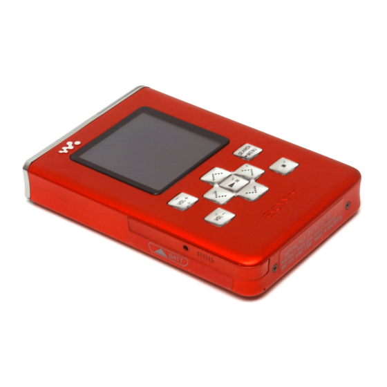
NW-HD5
SPECIFICATIONS
PORTABLE HARD DISK AUDIO PLAYER
US Model
AEP Model
UK Model
E Model
Australian Model
Chinese Model
Tourist Model
Supplied Accessories
Advertisement
Table of Contents

Related Manuals for Sony HW-HD5


Summary of Contents for Sony HW-HD5
- Page 1 UK Model E Model Australian Model Chinese Model Tourist Model SPECIFICATIONS Supplied Accessories PORTABLE HARD DISK AUDIO PLAYER Sony Corporation 9-879-662-04 Connect Company 2005F05-1 Published by Sony Engineering Corporation © 2005.06 For other Service and User Manuals, go to www.ManualDepot.com...
-
Page 2: Table Of Contents
COMPONENTS IDENTIFIED BY MARK 0 OR DOTTED LINE WITH MARK 0 ON THE SCHEMATIC DIAGRAMS AND IN THE PARTS LIST ARE CRITICAL TO SAFE OPERATION. REPLACE THESE COMPONENTS WITH SONY PARTS WHOSE PART NUMBERS APPEAR AS SHOWN IN THIS MANUAL OR IN SUPPLEMENTS PUBLISHED BY SONY. -
Page 3: Servicing Notes
NW-HD5 Ver. 1.3 SECTION 1 SERVICING NOTES SYSTEM REQUIREMENTS UNLEADED SOLDER Boards requiring use of unleaded solder are printed with the lead- free mark (LF) indicating the solder contains no lead. (Caution: Some printed circuit boards may not come printed with the lead free mark due to their particular size) : LEAD FREE MARK Unleaded solder has the following characteristics. -
Page 4: General
NW-HD5 SECTION 2 This section is extracted from instruction manual. GENERAL... -
Page 5: Disassembly
NW-HD5 SECTION 3 DISASSEMBLY • This set can be disassembled in the order shown below. 3-1. DISASSEMBLY FLOW 3-2. BATTERY CASE LID (Page 6) 3-3. CABINET (MAIN) BLOCK ASSY (Page 6) 3-4. CABINET (UPPER) BLOCK ASSY (Page 7) 3-5. HDD UNIT 3-6. -
Page 6: Battery Case Lid
NW-HD5 Note: Follow the disassembly procedure in the numerical order given. 3-2. BATTERY CASE LID... -
Page 7: Cabinet (Main) Block Assy
NW-HD5 3-4. CABINET (UPPER) BLOCK ASSY S5009 3 screw (M1.4) (EG) 2 screw (M1.4) knob (hold) 5 cabinet (upper) block assy 1 two screws (M1.4) 4 two screws (M1.4) 3-5. HDD UNIT 4 Remove the HDD unit section in the direction of arrow. 3 connector (HDD board) 5 insulator (L) -
Page 8: Main Board Section
NW-HD5 3-6. MAIN BOARD SECTION 3 claw 1 screw (M1.4) 5 two screws (M1.4) 2 claw 4 bracket (battery) section 9 MAIN board section 6 sheet (HDD FPC) 8 flexible board (CN2001) 3-7. MAIN BOARD 2 two hooks 5 LCD section 1 Remove two solders. -
Page 9: Position Of Ferrite Core
NW-HD5 3-8. POSITION OF FERRITE CORE -AC ADAPTOR- A cable is rolled twice. A cable is rolled twice. 40mm 40mm clamp filter (ferrite core) (Part No. 1-543-798-31) -USB CABLE- clamp filter (ferrite core) (Part No. 1-543-798-31) 50mm A cable is rolled onece. -
Page 10: Test Mode
NW-HD5 SECTION 4 TEST MODE 1. OUTLINE 5. OPERATION OF THE TEST MODE Power supply voltage : 3.65 to 3.75 V 5-1. Power Volume : 27 5-1-1. Power supply voltage check SOUND EQ : OFF This mode is used in case power supply voltage in the state where AVLS : OFF all power supply lines (1.2 V/1.5 V/1.9 V/2.4 V/3.3 V/VSTBY) are... - Page 11 NW-HD5 5-1-2. Consumption current (read state) check 5. Press the key, “WRITE” is displayed and hard disk drive becomes write state. This mode is used in case consumption current (read state) in the After 10 seconds, “FIN” is displayed automatically and write state where the hard disk drive has booted is checked.
- Page 12 NW-HD5 5. Press the key, “START” is displayed. Then automatically 5-2-3. Frequency characteristic check reboot (DC power supply state) or sleep (battery power supply “20 Hz/20 kHz/100 Hz/10 kHz 0 dBs L-ch/R-ch VOLUME: 27” state). audio signal is outputted. LCD display Checking method: 1.
- Page 13 NW-HD5 5-2-4. Channel separation check 5-2-6. SOUND EQ check “1 kHz 0 dBs L-ch/1 kHz 0 dBs R-ch VOLUME: 27” audio signal “100 Hz/250 Hz/630 Hz/1.6 kHz/4 kHz/10 kHz –20 dBs L-ch/R- is outputted. ch VOLUME: 27” audio signal is outputted. Checking method: Checking method: 1.
- Page 14 NW-HD5 7. Press the key, “START” is displayed and “10 kHz 0 dBs L- 14. Press the key, return to minor item selection screen. ch/R-ch VOLUME: 27” audio signal is outputted. In this state, 15. Press the [E] [e] key to select the “EQ 5”. each time [SEARCH/ MENU] key is pressed, Treble +3/–4/off LCD display...
- Page 15 NW-HD5 5-3. Others 4. Press the key, “START” is displayed. Then “OK” or “NG” 5-3-1. G-sensor check is displayed automatically. LCD display X/Y/Z-axis direction is checked. Checking method: START 1. Enter the test mode. 2. Press the [>] key to display major item, and press the [E] [e] key to select the “OTHERS”.
- Page 16 NW-HD5 5-3-4. LCD display check 5. “–X” is displayed. Main unit is fixed so that 2 of fig.1 may become downward and press the key. LCD display is checked. LCD display Checking method: 1. Enter the test mode. 2. Press the [>] key to display major item, and press the [E] [e] key to select the “OTHERS”.
- Page 17 NW-HD5 Ver. 1.3 5-3-6. G-sensor adjustment check 3. Press the [>] key to display minor item, and press the [E] [e] 4. Press the key. Press the [SEARCH/ MENU] key, 5-3-13. Factory setting key to select the “SC RD1” or “SC RD2” or “SC RDF”. destination (JP/US/EU/GA*) is selected.
-
Page 18: Diagrams
NW-HD5 SECTION 5 DIAGRAMS 5-1. BLOCK DIAGRAM – MAIN Section (1/2) – B+ SWITCH Q2001 VDC (MOTOR) HARD DISK VDC (LOGIC) +3.3V_HDD DRIVE UNIT (20GB) • SIGNAL PATH : AUDIO HDD_PWR_CTL (Page 20) IC1003 – IC7001 (Page 19) 72 73 74 77 78 83 84 85 80 148 146 143 142 144 145 147 141 140 47 48 49 50 51 52 53 54 57 58 59... -
Page 19: Block Diagram - Main Section (2/2)
NW-HD5 Ver. 1.3 5-2. BLOCK DIAGRAM – MAIN Section (2/2) – IC1003 – IC7001 (Page 18) • SIGNAL PATH : AUDIO 186 191 192 193 182 185 183 184 181 88 89 83 HEADPHONE AMP IC4301 D0 – 15 D0 – 15 (Page 18) DATA BUS AOUTL 134... -
Page 20: Block Diagram - Key/Power Supply Section
NW-HD5 5-3. BLOCK DIAGRAM – KEY/POWER SUPPLY Section – +2.4V_AD (IC1003) +2.4V +2.4V_DAC REGULATOR (IC1003) IC4302 +3.3V (IC4301) +3.3V_HD DC/DC CONVERTER IC9004 +3.3V_A PVIN +3.3V SVIN HDD_PWR_CTL BUFFER (Page 18) MODE Q9007 S5009 HOLD SHUT DOWN BUFFER SWITCH SHDN Q9008 Q9009 POWER CONTROL... - Page 21 NW-HD5 Ver. 1.3 • Note for Printed Wiring Boards and Schematic Diagrams • Waveform Note on Printed Wiring Board: Note on Schematic Diagram: – MAIN Board – • X : parts extracted from the component side. • All capacitors are in µF unless otherwise noted. (p: pF) •...
-
Page 22: Main Board (Component Side)
NW-HD5 Ver. 1.3 :Uses unleaded solder. 5-4. PRINTED WIRING BOARD – MAIN board (Component Side) – • Semiconductor Location Ref. No. Location D4101 MAIN BOARD (COMPONENT SIDE) D4201 D4301 D4302 TP9008 D4303 LF9001 D4304 L9004 L9006 D4445 D9004 FB9003 CN5002 D9001 SWITCH UNIT D9002... -
Page 23: Main Board (Conductor Side)
NW-HD5 Ver. 1.3 :Uses unleaded solder. 5-5. PRINTED WIRING BOARD – MAIN Board (Conductor Side) – • Semiconductor Location Ref. No. Location D5001 D5002 MAIN BOARD (CONDUCTOR SIDE) D5003 D9501 TP9010 TP9011 J9001 IC1001 (DC IN) IC1002 IC5001 IC9004 IC9502 TP9002 TP9011 IC9503... -
Page 24: Schematic Diagram - Main Board (1/7)
NW-HD5 • See page 35 for IC Pin Function Description. 5-6. SCHEMATIC DIAGRAM – MAIN Section (1/7) – (1/7) R7009 470k R7010 470k HDD_CNT USB_CNT RMC_DTCK BACKLIGHT_PWR (Page 26) XRESET_LCD XHDD_PWR_CTL XGSEN XGSEN_PWR_CTL XUSLEEP XUSLEEP XURESET R7003 R7004 R7008 XURESET (Page 28) USB_CNT R7001... -
Page 25: Schematic Diagram - Main Board (2/7)
NW-HD5 Ver. 1.3 • See page 32 for IC Block Diagram. 5-7. SCHEMATIC DIAGRAM – MAIN Section (2/7) – (2/7) GANDHI_CNT GAND_D GA17 GA17 ∗ IC1102 MBM29SL800BE -90PT FLASH MEMORY CSP(Chip Size Package) FLASH MEMORY ∗ (NOT SUPPLIED) IC1101 MBM29SL800BE GA16 -90PT CSP(Chip Size Package) -
Page 26: Schematic Diagram - Main Board (3/7)
NW-HD5 • See page 32 for IC Block Diagrams. 5-8. SCHEMATIC DIAGRAM – MAIN Section (3/7) – (3/7) USB_CNT CN5001 XUCS1 XRESET_LCD BACKLIGHT_PWR (Page 24) RMC_DTCK XUWR RW_WR XURD E_RD U_D0 U_D1 U_D2 U_D3 U_D4 U_D5 CN5002 LIQUID U_D6 CRYSTAL U_D7 STOP DISPLAY... -
Page 27: Schematic Diagram - Main Board (4/7)
NW-HD5 Ver. 1.3 • See page 21 for Waveform. • See page 35 for IC Pin Function Description. 5-9. SCHEMATIC DIAGRAM – MAIN Section (4/7) – (4/7) FS256 GAND_D GAND_A GANDHI_CNT XINTREQH R1026 TP1007 XINTREQH XINTREQG C1010 XINTREQG XINTREQU R1007 R1021 XINTREQU 100k... -
Page 28: Schematic Diagram - Main Board (5/7)
NW-HD5 • See page 32 for IC Block Diagram. • See page 35 for IC Pin Function Description. 5-10. SCHEMATIC DIAGRAM – MAIN Section (5/7) – (5/7) C8006 C8007 C8005 0.01 6.3V G-SENSOR B+ SWITCH IC8001 IC8000 SN74LVC1G66DCKR HAAM-312B DZOUT CSET DYOUT TP8002... -
Page 29: Schematic Diagram - Main Board (6/7)
NW-HD5 • See page 21 for Waveform. • See page 32 for IC Block Diagrams. • See page 35 for IC Pin Function Description. 5-11. SCHEMATIC DIAGRAM – MAIN Section (6/7) – (6/7) DATA+ CN9002 DATA- (Page 28) CONNECTOR VBUS FB9002 VBUS DATA+... -
Page 30: Schematic Diagram - Main Board (7/7)
NW-HD5 • See page 32 for IC Block Diagrams. 5-12. SCHEMATIC DIAGRAM – MAIN Section (7/7) – (7/7) 1.2V 1.2V 1.9V 1.9V 3.3V 3.3V XDCIN_DET BATT_MON_CTL BATT_MON_CTL PWR_FFCLR PWR_FFCLR C9042 C9036 C9034 C9033 C9035 C9038 PWR_SLEEP PWR_SLEEP 6.3V 6.3V 6.3V XRST XRST PWR_CLK... -
Page 31: Printed Wiring Board - Hdd Board
NW-HD5 5-13. PRINTED WIRING BOARD – HDD Section – :Uses unleaded solder. 5-14. SCHEMATIC DIAGRAM – HDD Section – HARD DISK DRIVE UNIT (20GB) HDD BOARD (COMPONENT SIDE) CN100 CN101 RESERVED RESERVED CN101 GND(LOGIC) GND(LOGIC) VDC(MOTOR) VDC(MOTOR) VDC(LOGIC) VDC(LOGIC) 1-866-844- (11) GND(MOTOR) GND(MOTOR) - Page 32 NW-HD5 • IC Block Diagrams – MAIN Board – IC3001 CXR710160-213GH IC4301 AN17020A-VB 64 63 62 61 60 59 58 57 56 55 52 51 50 49 PE3/RxD1 PE2/TxD1 BEEP PE1/RxD0 MUTING PE0/TxD0 HEADPHONE AMP − CH1 OUT LINE AMP CH1 IN HP/LINE PGND...
- Page 33 NW-HD5 IC8000 HAAM-312B DUTY CYCLE MODULATOR X SENSOR AMPLIFIER Y SENSOR Z SENSOR EEPROM IC9003 SC901584EPR2 36 35 RESET 2 SERIAL RST2 PASS POWER STEP REGULATOR 3 SWITCH 2 UP-DOWN REGC2 DRIVER RST2 MUTING REG2G REF2 VREF SERIAL BUFFER REGO2 PASS REGULATOR 2 REGI2...
- Page 34 NW-HD5 IC9004 LTC3411EDD#TR LOGIC BURST COMPARATOR HYSTERESIS = 80 mV SHDN/RT OSCILLATOR SYNC/MODE SGND ERROR AMPLIFIER NMOS +0.74V +0.86V COMPARATOR LIMIT REVERSE COMPARATOR PGND PGOOD VOLTAGE SVIN REFERENCE PMOS CURRENT COMPARATOR SLOPE COMPENSATION PVIN IC9503 R2061K01-E2 9 /INTR LEVEL SIO 1 SHIFTER SCLK 2 8 OSCOUT...
- Page 35 NW-HD5 • IC Pin Function Description MAIN BOARD IC1003 CXR704060-201GA (SYSTEM CONTROLLER, D/A CONVERTER) Pin No. Pin Name Description VDIO0 Power supply terminal (+1.9V) (for I/O interface) PM4/A12 to PM7/A15, 2 to 10 Address signal output to the flash memory and multi interface PN0/A16 to PN4/A20 PN5/A21 to...
- Page 36 NW-HD5 Pin No. Pin Name Description PE3/RXD1 Data input terminal Not used PE4/SCK1 Serial clock signal output to the power control and real time clock PE5/SO1 Serial data output to the power control and real time clock PE6/SI1 Serial data input from the real time clock PE7/SCS1 Chip enable signal output to the real time clock XOUT/CKO...
- Page 37 NW-HD5 Pin No. Pin Name Description PD2/DPLS Test terminal for debug Not used PD3/DMNS Test terminal for debug Not used PD4/TXDPLS Test terminal for debug Not used PD5/TXDMNS Test terminal for debug Not used PD6/TXENL Test terminal for debug Not used PD7/SUSPEND Test terminal for debug Not used VBUS...
- Page 38 NW-HD5 Ver. 1.3 Pin No. Pin Name Description MSINS Card detection signal input from the memory stick interface Not used HOLD key detection signal input terminal "L": hold P10/DADT Audio data input from the memory stick interface Not used P11/ADDT Audio data input from the sub system controller P12/LRCK L/R sampling clock signal input from the sub system controller...
- Page 39 NW-HD5 MAIN BOARD IC2001 1S1R72003BOOA100 (USB CONTROLLER) Pin No. Pin Name Description Internal operation setting terminal N.C. Not used AVSS Ground terminal (analog system) AVDD Power supply terminal (+3.3V) (analog system) AVSS Ground terminal (analog system) AVDD Power supply terminal (+3.3V) (analog system) AVSS Ground terminal (analog system) USB data (+) input/output terminal...
- Page 40 NW-HD5 Pin No. Pin Name Description HIORDY Wait signal input from the hard disk drive unit Ground terminal (logic system) Power supply terminal (+3.3V) (logic system) XHDMACK DMA acknowledge signal output to the hard disk drive unit HINTRQ Interrupt request signal input from the hard disk drive unit Address signal output to the multi interface and hard disk drive unit XHPDIAG Diagnosis sequence compression signal input from the hard disk drive unit...
- Page 41 NW-HD5 MAIN BOARD IC7001 CXD1616GH (MULTI INTERFACE) Pin No. Pin Name Description XTAL Sub system clock input terminal Not used EXTAL Sub system clock output terminal Not used CLK2550A Clock signal (22.5792 MHz) output terminal Not used CLK2550X Clock signal (22.5792 MHz) inversion output terminal Not used XOSCSTP Oscillation stop signal input terminal Not used XRESET...
- Page 42 NW-HD5 Pin No. Pin Name Description HIORDY Wait signal input from the hard disk drive unit XHDMACK DMA acknowledge signal output to the hard disk drive unit HDMARQ DMA request signal input from the hard disk drive unit HINTREQ Interrupt request signal input from the hard disk drive unit XHRESET Reset signal output to the hard disk drive unit LRCK...
- Page 43 NW-HD5 MAIN BOARD IC9002 SN412005RHLR (CHARGE CONTROL) Pin No. Pin Name Description 3.3V LDO regurated power supply output terminal ISTAT1 Charge progress signal output to the system controller "L": charge state ISTAT2 Charge completion signal output to the system controller Charge volatage input from the AC adaptor Power supply volatage input from the rechargeable battery or charge volatage output to the 5, 6...
-
Page 44: Exploded View
NW-HD5 Ver. 1.3 SECTION 6 EXPLODED VIEWS NOTE: • -XX and -X mean standardized parts, so they • Items marked “*” are not stocked since they may have some difference from the original are seldom required for routine service. Some one. -
Page 45: Main Section
NW-HD5 Ver. 1.3 6-2. MAIN SECTION MAIN board Ref. No. Part No. Description Remark Ref. No. Part No. Description Remark 2-594-386-01 SHAFT (BATTERY CASE LID) 2-634-752-01 CUSHION, HDD 1.5B 2-594-385-01 BRACKET (BATTERY) 3-238-876-04 SCREW (M1.4), TOOTHED LOCK 2-629-604-01 CUSHION (HDD 1.5) 2-594-368-01 HINGE (BATTERY CASE LID) (for SILVER) 2-629-604-31 CUSHION (HDD 1.5) 2-594-368-11 HINGE (BATTERY CASE LID) (for BLACK) -
Page 46: Electrical Parts List
NW-HD5 Ver. 1.3 SECTION 7 MAIN ELECTRICAL PARTS LIST NOTE: • Due to standardization, replacements in the • Items marked “*” are not stocked since they The components identified by mark 0 or dotted line with mark 0 are parts list may be different from the parts are seldom required for routine service. - Page 47 NW-HD5 MAIN Ref. No. Part No. Description Remark Ref. No. Part No. Description Remark C7010 1-100-504-11 CERAMIC CHIP 0.1uF 6.3V C3008 1-100-504-11 CERAMIC CHIP 0.1uF 6.3V C7011 1-128-617-11 CERAMIC CHIP 100PF C3009 1-100-504-11 CERAMIC CHIP 0.1uF 6.3V C7012 1-100-504-11 CERAMIC CHIP 0.1uF 6.3V C3010...
- Page 48 NW-HD5 Ver. 1.3 MAIN Ref. No. Part No. Description Remark Ref. No. Part No. Description Remark FB7003 1-218-990-11 SHORT CHIP C9509 1-100-504-11 CERAMIC CHIP 0.1uF 6.3V FB7004 1-218-990-11 SHORT CHIP C9510 1-164-842-11 CERAMIC CHIP 0.25PF 50V FB9001 1-216-864-11 SHORT CHIP <...
- Page 49 NW-HD5 Ver. 1.3 MAIN Ref. No. Part No. Description Remark Ref. No. Part No. Description Remark R2023 1-218-965-11 RES-CHIP 1/16W < RESISTOR > R2024 1-218-965-11 RES-CHIP 1/16W R2025 1-218-965-11 RES-CHIP 1/16W R1001 1-218-985-11 RES-CHIP 470K 1/16W R1002 1-218-990-11 SHORT CHIP R2026 1-218-935-11 RES-CHIP 1/16W...
- Page 50 NW-HD5 MAIN Ref. No. Part No. Description Remark Ref. No. Part No. Description Remark R4313 1-218-953-11 RES-CHIP 1/16W R9025 1-218-985-11 RES-CHIP 470K 1/16W R4315 1-218-990-11 SHORT CHIP R9026 1-208-703-11 METAL CHIP 6.8K 0.5% 1/16W R4316 1-218-933-11 RES-CHIP 1/16W R5001 1-216-798-11 METAL CHIP 1/10W R9027 1-218-985-11 RES-CHIP...
- Page 51 NW-HD5 Ver. 1.3 MAIN Ref. No. Part No. Description Remark Ref. No. Part No. Description Remark < VIBRATOR > X1002 1-795-891-21 VIBRATOR, CERAMIC (22.5792MHz) X2001 1-813-362-11 VIBRATOR, CRYSTAL (12MHz) X3001 1-795-891-21 VIBRATOR, CERAMIC (22.579MHz) X9501 1-795-602-11 VIBRATOR, CRYSTAL (32.768kHz) ************************************************************ MISCELLANEOUS ************** X-2059-912-1 LITHIUM ION BATTERY ASSY (US)
-
Page 52: Revision History
NW-HD5 REVISION HISTORY Clicking the version allows you to jump to the revised page. Also, clicking the version at the upper right on the revised page allows you to jump to the next revised page. Ver. Date Description of Revision 2005.04 2005.05 Addition of E, Korean and Australian models...