Sony Walkman NW-S202 Service Manual
Digital music player
Hide thumbs
Also See for Walkman NW-S202:
- Quick start manual (16 pages) ,
- Operation manual (93 pages) ,
- Notes on usage (4 pages)
Table of Contents
Advertisement
NW-S202/S202F/S203F/S205F
SERVICE MANUAL
Ver. 1.2 2006.11
• SonicStage and the SonicStage logo are trademarks or registered trademarks of Sony Corporation.
• OpenMG, ATRAC, ATRAC3, ATRAC3plus and their logos are trademarks of Sony Corporation.
• "WALKMAN" and "WALKMAN" logo are registered trademarks of Sony Corporation.
• Microsoft, Windows, Windows NT and Windows Media are trademarks or registered trademarks of Microsoft Corporation in the United States and/or other countries.
• Adobe and Adobe Reader are trademarks or registered trademarks of Adobe Systems Incorporated in the United States and/or other countries.
• MPEG Layer-3 audio coding technology and patents licensed from Fraunhofer IIS and Thomson.
• IBM and PC/AT are registered trademarks of International Business Machines Corporation.
• Macintosh is a trademark of Apple Computer, Inc.
• Pentium is a trademark or a registered trademark of Intel Corporation.
• CD and music-related data from Gracenote, Inc., copyright
®
Gracenote CDDB
Client Software, copyright 2000-2004 Gracenote. This product and service may practice one or more of the following U.S. Patents: #5,987,525; #6,061,680;
#6,154,773, #6,161,132, #6,230,192, #6,230,207, #6,240,459, #6,330,593, and other patents issued or pending. Services supplied and/or device manufactured under license for following
Open Globe,Inc. United States Patent 6,304,523. Gracenote and CDDB are registered trademarks of Gracenote.
The Gracenote logo and logotype, and the "Powered by Gracenote" logo are trademarks of Gracenote.
• All other trademarks and registered trademarks are trademarks or registered trademarks of their respective holders. In this manual,
Audio compression technology
– MPEG-1 Audio Layer-3 (MP3)
*
– Windows Media Audio (WMA)
– Adaptive Transform Acoustic Coding (ATRAC)
*
– Advanced Audio Coding (AAC)
* WMA/AAC format audio files that are copyright-protected cannot be played back.
Maximum recordable number of songs and time (Approx.)*
* The approximate times are based on a transferred 4-minute ATRAC or MP3 format song. Other playable audio file
formats may be different from ATRAC or MP3 format.
NW-S202F/S202
Bit rate
Songs
Time
48 kbps
340
22 hr. 40 min.
64 kbps
255
17 hr. 00 min.
96 kbps
170
11 hr. 20 min.
128 kbps
125
8 hr. 20 min.
132 kbps
120
8 hr. 00 min.
160 kbps
100
6 hr. 40 min.
192 kbps
85
5 hr. 40 min.
256 kbps
64
4 hr. 10 min.
320 kbps
51
3 hr. 20 min.
352 kbps
46
3 hr. 00 min.
Sony Corporation
9-887-385-03
Connect Business Division
2006K05-1
C
2006.11
Published by Sony Techno Create Corporation
Photo: NW-S203F
©
2000-2004 Gracenote.
SPECIFICATIONS
NW-S203F
Songs
Time
685
45 hr. 00 min.
515
34 hr. 20 min.
345
23 hr. 00 min.
260
17 hr. 20 min.
250
16 hr. 40 min.
205
13 hr. 40 min.
170
11 hr. 20 min.
130
8 hr. 40 min.
100
6 hr. 40 min.
94
6 hr. 10 min.
Canadian Model
Australian Model
NW-S202/S202F/S203F/S205F
TM
®
and
NW-S205F
Bit rate
Songs
Time
48 kbps
1,350
90 hr. 00 min.
64 kbps
1,000
66 hr. 40 min.
96 kbps
690
46 hr. 00 min.
128 kbps
520
34 hr. 40 min.
132 kbps
500
33 hr. 20 min.
160 kbps
415
27 hr. 40 min.
192 kbps
345
23 hr. 00 min.
256 kbps
260
17 hr. 20 min.
320 kbps
205
13 hr. 40 min.
352 kbps
185
12 hr. 20 min.
Capacity (User available capacity)*
NW-S202F/S202: 512 MB (Approx. 482 MB = 505,724,928 bytes)
NW-S203F: 1 GB (Approx. 968 MB = 1,015,726,080 bytes)
NW-S205F: 2 GB (Approx. 1.89 GB = 2,035,974,144 bytes)
* Available storage capacity of the player may vary.
A portion of the memory is used for data management functions.
Supported bit rates
MP3: 32 to 320 kbps variable bit rate-compliant
WMA: 32 to 192 kbps variable bit rate-compliant
ATRAC: 48/64/66 (ATRAC3)*/96/105 (ATRAC3)*/128/132 (ATRAC3)/160/192/256/320/352 kbps
* CD recording cannot be done using SonicStage software in ATRAC3 at 66/105 kbps.
AAC: 16 to 320 kbps variable bit rate-compliant*
* Nonstandard bit rates or non-guaranteed bit rates are included depending on the sampling frequency.
DIGITAL MUSIC PLAYER
US Model
E Model
Tourist Model
NW-S203F/S205F
AEP Model
UK Model
Chinese Model
NW-S202F/S203F/S205F
marks are not specifi ed.
- Continued on next page -
Advertisement
Table of Contents

Related Manuals for Sony Walkman NW-S202


Summary of Contents for Sony Walkman NW-S202
-
Page 1: Specifications
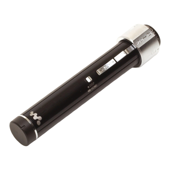
NW-S202F/S203F/S205F Photo: NW-S203F • SonicStage and the SonicStage logo are trademarks or registered trademarks of Sony Corporation. • OpenMG, ATRAC, ATRAC3, ATRAC3plus and their logos are trademarks of Sony Corporation. • “WALKMAN” and “WALKMAN” logo are registered trademarks of Sony Corporation. -
Page 2: Table Of Contents
NW-S202/S202F/S203F/S205F TABLE OF CONTENTS Sampling frequency* MP3: 32, 44.1, 48 kHz SERVICING NOTES ..........3 WMA: 44.1 kHz ATRAC: 44.1 kHz AAC: 11.025, 12, 16, 22.05, 24, 32, 44.1, 48 kHz * Sampling frequency may not correspond to all encoders................ -
Page 3: Servicing Notes
NW-S202/S202F/S203F/S205F SECTION 1 Ver. 1.1 SERVICING NOTES UNLEADED SOLDER Minimum System Requirements (for the player) Computer Boards requiring use of unleaded solder are printed with the lead- IBM PC/AT or compatible computer preinstalled with the following Windows operating systems: – Windows 2000 Professional (Service Pack 3 or later) free mark (LF) indicating the solder contains no lead. - Page 4 NW-S202/S202F/S203F/S205F Ver. 1.2 COLOR VARIATION COLOR Model Destination BLACK SILVER PINK NW-S202 CEW (Clamshell) CEW (Clamshell) NW-S202F US (Clamshell) CND (Clamshell) CEW (Clamshell) NW-S203F E, AUS, JE US (Clamshell) CND (Clamshell) CEW (Clamshell) NW-S205F E, AUS, JE • Abbreviation : Australian model : East European model CEW : AEP, UK models : Chinese model...
-
Page 5: General
NW-S202/S202F/S203F/S205F SECTION 2 This section is extracted from GENERAL instruction manual. HOLD function ��Shuttle switch Parts and Controls You can protect the player against By rotating the shuttle switch, you can accidental operation by using the select a menu item, skip to the HOLD function when carrying it. -
Page 6: Disassembly
NW-S202/S202F/S203F/S205F SECTION 3 DISASSEMBLY • This is can be disassembly in the order shown below. 3-1. DISASSEMBLY FLOW 3-2. HP CAP (INNER) (Page 6) 3-3. WINDOW (Page 7) 3-4. USB HOLDER (Page 7) 3-5. PANEL (SUB ASSY) (Page 8) 3-6. ORGANIC EL INDICATOR MODULE (EL401), MAIN BOARD (Page 8) 3-7. -
Page 7: Window
NW-S202/S202F/S203F/S205F 3-3. WINDOW composition of parts click plate shuttle (SVX) assy Note: Adhesive sheet (window) cannot be re-used. Please replace to brand-new part once adhesive sheet (window) is removed. spring (shuttle) sheet (shuttle ESD) 5 adhesive sheet (window) click plate cushion (shuttle) click plate shuttle (SVX) assy... -
Page 8: Panel (Sub Assy)
NW-S202/S202F/S203F/S205F 3-5. PANEL (SUB ASSY) 3 panel (sub assy) 1 screw (M1.4 × 2.0) 2 two pins (case) 3-6. ORGANIC EL INDICATOR MODULE (EL401), MAIN BOARD 6 OEL holder 5 two pins (USB) 8 connector (CN501) 4 Lift the organic EL indicator module (EL401) to remove the pins (USB). -
Page 9: Chassis
NW-S202/S202F/S203F/S205F 3-7. CHASSIS Note: Sheet (headphone jack) cannot 2 bracket USB be re-used. 3 copper sheet Please replace to brand-new parts once (plate PWB) sheets (headphone jack) are removed. sheet (headphone jack) 4 HEADPHONE board (ground portion) 1 battery (A) assy (lithium ion battery) 7 chassis assy chassis assy... -
Page 10: Test Mode
NW-S202/S202F/S203F/S205F SECTION 4 Ver. 1.1 TEST MODE SETTING THE TEST MODE 2-3. ALL Key Check When all keys and the shuttle switches are correctly input, the set Supply power to the set, While pressing the B x key, press the key as following order. -
Page 11: Diagrams
NW-S202/S202F/S203F/S205F SECTION 5 DIAGRAMS 5-1. BLOCK DIAGRAM AOUTL HPINL HPOUTL J901 CN101 AOUTR 73 HPINR HPOUTR (HEADPHONE) (USB CONNECTOR) VBUS (S202F/S203F/S205F) TUNER IC2702 MICINL AOUT_L MICINR 186 AOUT_R +2.7V SIO/GPIOG1 REGULATOR VDD IO +2.8V SO0/GPIOG0 133 X101 IC2701 SCK0 134 12MHz SCS0/GPIOG2 GATE... - Page 12 NW-S202/S202F/S203F/S205F • IC Block Diagrams – MAIN Board – THIS NOTE IS COMMON FOR PRINTED WIRING BOARDS AND SCHEMATIC DIAGRAMS. IC201 S71PL032J04BFWOBOB For Schematic Diagrams. For Printed Wiring Boards. Note: Note: • All capacitors are in µF unless otherwise noted. (p: pF) •...
- Page 13 NW-S202/S202F/S203F/S205F IC801 3 AXIS ACCELEROMETER X801 RX-4574LC 32.768KHz CONTROL LINE N.C. DIVIDER 20 19 18 17 16 15 N.C. CLOCK AND CALENDAR /TIRQ TOUT /AIRQ AGND FCON TIMER OUTPUT REGISTER FOUT CONTROLLER X SENSOR ALARM REGISTER INTERRUPTS Y SENSOR CONTROLLER CONTROL Z SENSOR REGISTER...
-
Page 14: Printed Wiring Board - Main Board
NW-S202/S202F/S203F/S205F Ver. 1.1 5-2. PRINTED WIRING BOARD – MAIN board – : Uses unleaded solder. MAIN BOARD (SIDE A) (S202F/S203F/S205F) C2707 C610 C2708 IC902 (S202F/S203F/S205F) C616 JL301 JL114 JL602 R2115 R619 C803 R901 C120 C119 R110 R203 C145 L602 C607 JL616 R806 R804... -
Page 15: Printed Wiring Board - Switch Board
NW-S202/S202F/S203F/S205F 5-3. PRINTED WIRING BOARD – SWITCH Board – : Uses unleaded solder. SWITCH BOARD (SIDE A) R510 VDR503 R508 R503 R517 VDR502 R516 S504 S502 S503 S501 VDR501 (11) 1-871-611- R509 S504 S502 S503 S501 – DISP HOME SWITCH BOARD (SIDE B) CN501 MAIN BOARD... -
Page 16: Schematic Diagram - Main Section (1/3)
NW-S202/S202F/S203F/S205F Ver. 1.1 5-4. SCHEMATIC DIAGRAM – MAIN Section (1/3) – • See page 21 for IC Pin Function Description. MAIN BOARD (1/3) (S202F/S203F/S205F) C2117 0.022 R2107 8200 C2112 0.022 R2106 8200 (Page 17) VDD_RTC2.8 VDD_RTC2.8 RTC_CE TU_OUTL RTC_CE MAIN RTC_SCK (Page 17) RTC_SCK... -
Page 17: Schematic Diagram - Main Section (2/3)
NW-S202/S202F/S203F/S205F Ver. 1.1 5-5. SCHEMATIC DIAGRAM – MAIN Section (2/3) – • See page 12 for IC Block Diagrams. MAIN BOARD (2/3) R2711 4700 (S202F/S203F/S205F) TU_STO MAIN BOARD VDD_IO2.8 (3/3) TU_SCK (Page 18) R2710 TU_LA MAIN R2702 BOARD MAIN 6800 (Page 16) DGND R2701... -
Page 18: Schematic Diagram - Main Section (3/3)
NW-S202/S202F/S203F/S205F 5-6. SCHEMATIC DIAGRAM – MAIN Section (3/3) – • See page 12 for IC Block Diagrams. MAIN BOARD (3/3) C608 JL619 VDR602 R617 R611 JL614 470k Q604 C626 2SK354700LS0 B+ SWITCH IC B/D VCORE_XUP C627 1000p MAIN BOARD (1/3) (Page C625 R631... -
Page 19: Printed Wiring Board - Headphone Board
NW-S202/S202F/S203F/S205F 5-7. PRINTED WIRING BOARD – HEADPHONE Board – : Uses unleaded solder. (Page 14) MAIN BOARD CN102 HEADPHONE BOARD HEADPHONE BOARD (COMPONENT SIDE) (CONDUCTOR SIDE) FB903 X901 X902 J901 (HEADPHONE) X904 X903 FB902 FB901 JL931 D901 (CHASSIS) JL921 VDR901 VDR902 IC901 C901... -
Page 20: Schematic Diagram - Headphone Board
NW-S202/S202F/S203F/S205F 5-8. SCHEMATIC DIAGRAM – HEADPHONE Board – • See page 12 for IC Block Diagrams. HEADPHONE BOARD IC B/D X901 HALL X902 HE2N HALL IC901 HALL ELEMENT DRIVER IC901 AK8981 HE1N JL921 X903 RESERVE HALL C903 VDD_IO 100p C902 220p X904 HALL... - Page 21 NW-S202/S202F/S203F/S205F Ver. 1.1 • IC Pin Function Description MAIN BOARD IC101 CXD5090B1-003GG (SYSTEM CONTROLLER, NAND FLASH INTERFACE, USB INTERFACE, A/D, D/A CONVERTER, SERIAL INTERFACE) Pin No. Pin Name Description NAD0/GPIOC0 1 to 8 to NAD7/ Data signal input from the NAND flash ROM GPIOC7 NCLE/GPIOC8 Command latch enable signal output to the NAND flash ROM...
- Page 22 NW-S202/S202F/S203F/S205F Pin No. Pin Name Description SCL/GPIOK0 Chip select output to the hall element driver SDA/GPIOK1 Serial data input/output terminal Not used EC0/INT6/ Model setting terminal Not used GPIOL0 T1/GPIOL1 ON/OFF control signal output to the 3 axis accelerometer EC2/INT7/ Not used GPIOL2 T3/GPIOL3...
- Page 23 NW-S202/S202F/S203F/S205F Pin No. Pin Name Description SDDAT3/INT5/ Reset signal output to the organic EL indicator module GPIOF4 Ground terminal DVDIO2 Power supply terminal DVDK2 Power supply terminal Ground terminal DVDIO2 Power supply terminal Ground terminal MSBS/INT0/ Not used GPIOE0 MSSCLK Not used MSDIO0/ Not used...
- Page 24 NW-S202/S202F/S203F/S205F Pin No. Pin Name Description SI0/GPIOG1 Status signal input from the tuner and hall element driver SO0/GPIOG0 Serial data output to the tuner and hall element driver SCK0 Serial data transfer clock signal output to the tuner and hall element driver SCS0/GPIOG2 Serial latch pulse signal output to the tuner SI1/GPIOH1...
- Page 25 NW-S202/S202F/S203F/S205F Pin No. Pin Name Description DVDK2 Power supply terminal Ground terminal 195 to 199 A17 to A21 Address signal output to the flash ROM, SRAM Address signal output terminal Not used A23/GPIOA1 Address signal output terminal Not used A24/GPIOA2 Model setting terminal Not used A25/GPIOA3 Model setting terminal Not used...
- Page 26 NW-S202/S202F/S203F/S205F Pin No. Pin Name Description SOURCE Power supply terminal GATE Power supply ON/OFF control signal input terminal for the NAND flash ROM CRST1A System reset signal input terminal CRST1B Reset signal input terminal Not used RST1VDD Power supply terminal RST1AOUT System reset signal output terminal RST1BOUT...
-
Page 27: Exploded Views
NW-S202/S202F/S203F/S205F SECTION 6 Ver. 1.1 EXPLODED VIEWS NOTE: • -XX and -X mean standardized parts, so they • Items marked “*” are not stocked since they • Abbreviation may have some difference from the original are seldom required for routine service. Some AUS : Australian model one. -
Page 28: Usb Holder Section
NW-S202/S202F/S203F/S205F Ver. 1.1 6-2. USB HOLDER SECTION panel section Note: When the set is resolved, perform “Hall Calib.” (Refer to page 10) of the test mode after assembling the set. Ref. No. Part No. Description Remark Ref. No. Part No. Description Remark 2-886-056-01... -
Page 29: Panel Section
NW-S202/S202F/S203F/S205F Ver. 1.2 6-3. PANEL SECTION main section Note: When the set is resolved, perform “Hall Calib.” (Refer to page 10) of the test mode after assembling the set. Ref. No. Part No. Description Remark Ref. No. Part No. Description Remark 2-887-807-01 PIN (CASE) -
Page 30: Main Section
NW-S202/S202F/S203F/S205F Ver. 1.1 Note: When the set is resolved, perform “Hall Calib.” (Refer to page 10) of the test mode after assembling the set. 6-4. MAIN SECTION J901 EL401 Note: When the MAIN board is replaced, format it according to the “NOTE THE MAIN BOARD REPLACING”... -
Page 31: Electrical Parts List
NW-S202/S202F/S203F/S205F SECTION 7 Ver. 1.1 HEADPHONE MAIN ELECTRICAL PARTS LIST NOTE: • Due to standardization replacements in the • RESISTORS • Abbreviation parts list may be different from the parts All resistors are in ohms. AUS : Australian model specified in the diagrams or the components METAL : Metal-film resistor. - Page 32 NW-S202/S202F/S203F/S205F Ver. 1.1 MAIN Ref. No. Part No. Description Remark Ref. No. Part No. Description Remark C141 1-125-777-11 CERAMIC CHIP 0.1uF C901 1-100-735-91 CERAMIC CHIP 10uF C142 1-100-735-91 CERAMIC CHIP 10uF C902 1-125-777-11 CERAMIC CHIP 0.1uF C1301 1-100-504-11 CERAMIC CHIP 0.1uF 6.3V C143 1-112-692-11...
- Page 33 NW-S202/S202F/S203F/S205F MAIN Ref. No. Part No. Description Remark Ref. No. Part No. Description Remark IC1301 (Not supplied) IC TC58NVG3D4CTGOO (S203F) R513 1-240-718-91 METAL CHIP 100K 1/20W IC1301 (Not supplied) IC TH58NVG4D4CTGOO (S205F) R514 1-240-707-91 METAL CHIP 1/20W IC1301 (Not supplied) IC HY27UF084G2M-TPCB (S202/S202F) R516 1-218-965-11...
- Page 34 NW-S202/S202F/S203F/S205F Ver. 1.2 MAIN SWITCH Ref. No. Part No. Description Remark Ref. No. Part No. Description Remark < VARISTOR > MISCELLANEOUS ************** VDR101 1-805-216-21 VARISTOR, CHIP VDR102 1-805-216-21 VARISTOR, CHIP 1-756-686-11 LITHIUM ION BATTERY (S202/S202F/S203F: VDR105 1-803-742-21 VARISTOR, CHIP CEW, CEV, E, MX, KR, AUS, CH, JE/ VDR106 1-803-742-21 VARISTOR, CHIP S205F: CEW, CEV, E, MX, KR, AUS, CH, JE)
- Page 35 NW-S202/S202F/S203F/S205F US Model Canadian Model SERVICE MANUAL E Model Australian Model Tourist Model Ver. 1.2 2006.11 NW-S203F/S205F AEP Model UK Model NW-S202/S202F/S203F/S205F SUPPLEMENT-1 Chinese Model NW-S202F/S203F/S205F File this supplement with the service manual. Subject : Change of MAIN board (Suffi x-12) In this set, MAIN board has been changed in the midway of production.
- Page 36 NW-S202/S202F/S203F/S205F 2. DIAGRAMS THIS NOTE IS COMMON FOR PRINTED WIRING BOARDS AND SCHEMATIC DIAGRAMS. For Schematic Diagrams. For Printed Wiring Boards. Note: Note: • All capacitors are in µF unless otherwise noted. (p: pF) • X : parts extracted from the component side. 50 WV or less are not indicated except for electrolytics and •...
- Page 37 NW-S202/S202F/S203F/S205F 2-1. PRINTED WIRING BOARD – MAIN board – : Uses unleaded solder. MAIN BOARD (SIDE A) (S202F/S203F/S205F) C2707 C610 C2708 IC902 (S202F/S203F/S205F) C616 JL301 JL114 JL602 R2115 R619 C803 R901 C120 C119 R110 R203 C145 L602 C607 JL616 R806 R804 R111 C162...
- Page 38 NW-S202/S202F/S203F/S205F 2-2. SCHEMATIC DIAGRAM – MAIN Section (1/3) – MAIN BOARD (1/3) (S202F/S203F/S205F) C2117 0.022 R2107 8200 C2112 0.022 R2106 8200 (Page 5) VDD_RTC2.8 VDD_RTC2.8 RTC_CE TU_OUTL RTC_CE MAIN RTC_SCK (Page 5) RTC_SCK BOARD TU_OUTR (2/3) RTC_SI RTC_SI MAIN RTC_SO BOARD RTC_SO (2/3)
- Page 39 NW-S202/S202F/S203F/S205F 2-3. SCHEMATIC DIAGRAM – MAIN Section (2/3) – MAIN BOARD (2/3) R2711 4700 (S202F/S203F/S205F) TU_STO MAIN BOARD VDD_IO2.8 (3/3) TU_SCK (Page 6) R2710 TU_LA MAIN R2702 BOARD MAIN 6800 (Page 4) DGND R2701 4700 (1/3) BOARD (Page 4) TU_CLKON (1/3) R2706 BIU_D15...
- Page 40 NW-S202/S202F/S203F/S205F 2-4. SCHEMATIC DIAGRAM – MAIN Section (3/3) – MAIN BOARD (3/3) C608 JL619 VDR602 R617 R611 JL614 470k Q604 C626 2SK354700LS0 B+ SWITCH VCORE_XUP C627 1000p MAIN BOARD (1/3) (Page C625 R631 470k PWR_ON1 USB_SUS (Page 4) R633 PG_CORE JL603 L601 USB_H/L...
- Page 41 NW-S202/S202F/S203F/S205F MAIN 3. ELECTRICAL PARTS LIST NOTE: • Due to standardization replacements in the • RESISTORS • Abbreviation parts list may be different from the parts All resistors are in ohms. AUS : Australian model specified in the diagrams or the components METAL : Metal-film resistor.
- Page 42 NW-S202/S202F/S203F/S205F MAIN Ref. No. Part No. Description Remark Ref. No. Part No. Description Remark C602 1-112-815-91 CERAMIC CHIP 10uF 6.3V C603 1-112-815-91 CERAMIC CHIP 10uF 6.3V < DIODE > C604 1-131-664-91 CERAMIC CHIP 0.15uF D401 6-501-386-01 DIODE MA21D3800LS0 C605 1-125-777-11 CERAMIC CHIP 0.1uF D601 8-719-069-29...
- Page 43 NW-S202/S202F/S203F/S205F MAIN Ref. No. Part No. Description Remark Ref. No. Part No. Description Remark R113 1-218-990-11 SHORT CHIP R808 1-218-979-11 RES-CHIP 150K 1/16W R114 1-218-990-11 SHORT CHIP R809 1-218-978-11 RES-CHIP 120K 1/16W R901 1-218-989-11 RES-CHIP 1/16W R116 1-218-977-11 RES-CHIP 100K 1/16W R902 1-218-989-11...
-
Page 44: Revision History
NW-S202/S202F/S203F/S205F REVISION HISTORY Clicking the version allows you to jump to the revised page. Also, clicking the version at the upper right on the revised page allows you to jump to the next revised page Ver. Date Description of Revision 2006.08 2006.10 Addition of Chinese model (NW-S202F/S203F/S205F)