Sign In
Upload
Manuals
Brands
Tektronix Manuals
Measuring Instruments
DAS9100
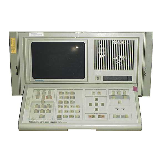
Tektronix DAS9100 Manuals
Manuals and User Guides for Tektronix DAS9100. We have
2
Tektronix DAS9100 manuals available for free PDF download: Service Manual, Service Notes
Tektronix DAS9100 Service Manual (507 pages)
Brand:
Tektronix
| Category:
Measuring Instruments
| Size: 12.46 MB
Table of Contents
Table of Contents
8
Description
29
Modes of Operation
29
Data Acquisition
29
Acquisition and Reference Memory Display
30
Pattern Generation
30
GPIB, RS-232, and Hard Copy Interface
31
Tape Drive
31
Mainframe Standard Components
31
GPIB, RS-232, and Hard Copy Interfaces
31
DAS9109 Mainframe Configuration
33
Instrument Modules
34
Mainframe Options
35
Standard and Optional Accessories
36
Mainframe
36
A32 Data Acquisition Module
37
91A32 Data Acquisition Module
37
A08 Data Acquisition Module
37
P16 Pattern Generator Module
37
P32 Pattern Generator Expander Module
38
P6452 Data Acquisition Probe
38
P6454 100 Mhz Clock Probe
38
DAS9129 and DAS9109 Electrical Specifications: Mainframe Power
40
Specifications
40
DAS9129 Electrical Specifications: Color Display Monitor
42
DAS9109 Electrical Specifications: CRT Monochrome Display Monitor
44
DAS9129 and DAS9109 Electrical Specifications: Keyboard
45
DAS9109 Electrical Specifications: Controller Module
45
Character and Waveform Sets
47
DAS9129 and DAS9109 Physical Specifications
50
A08 Electrical Specifications: Power
55
91A08 Electrical Specifications: Data Acquisition and Storage
55
Pattern Generator Modules
59
P6452 Data Acquisition Probe
64
P6452 Electrical Specifications
64
P6452 Environmental Specifications
65
P6452 Physical Specifications
66
P6454 100 Mhz Clock Probe
67
P6454 Electrical Specifications
67
P6454 Environmental Specifications
68
P6455 Ttl/Mas Pattern Generator Probe
69
P6454 Physical Specifications
69
P6455 Electrical Specifications
69
P6455 Environmental Specifications
71
P6456 Ecl Pattern Generator Probe
72
P6455 Physical Specifications
72
P6456 Electrical Specifications
72
P6456 Environmental Specifications
73
P6456 Physical Specifications
74
Option 01, Tape Drive Assembly
75
Tape Drive Electrical Specifications
75
Tape Drive Environmental Specifications
77
Tape Drive Physical Specifications
78
I/O Interface Electrical Specifications: Power
79
Option 02, I/O Interface Assembly
79
I/O Interface Electrical Specifications: RS-232 Lines
80
Overall Dimensions of the DAS9129 and DAS9109 Mainframes
81
I/O Interface Electrical Specifications: Composite Video
81
Instrument Module Dimensions
82
P6452, P6455, P6456 Dimensions
84
Option 01, Tape Drive
88
Option 02, I/O Interface
88
Power Supply
88
Option 04, Two 5 V Power Supplies
89
Option 05, Rackmount Hardware
89
Mainframe Configuration
90
Power Requirements
91
Location of the Line-Voltage Indicator
91
Power Cords
92
Optional das 9100 Power Cords
92
Mainframe Ground
93
Configuration Guidelines
93
Location of the Mainframe Ground Connector
93
Internal Structure of the das Mainframe
94
Module Configuration Label
95
Configuration Guidelines
95
Probe Connections
96
Connecting a Probe to the das
96
Location of the Module Configuration Label
96
Pod 10
97
DAS Probes and Their Pod Connections
97
Connecting a Probe to a Pod Connector
98
P6452 External Clock Probe
100
External Clock Probe Signal Lines
100
Pod ID
100
P6452 Data Acquisition Probe
101
P6452 Data Acquisition Probe
103
P6454 100 Mhz Clock Probe
104
P6455 Ttl/Mas Pattern Generator Probe
106
Standard and Optional I/O Connectors
109
Word Recognizer Output and Trigger Input Connectors
109
Location of the Word Recognizer Output and Trigger Input Connectors
109
Tape Drive Controls
110
Rs-232 Interface
110
General Purpose Interface Bus (GPIB)
111
GPIB Connectors and Indicators
112
Video Composite Output
113
Color Monitor Controls (Das9129 Color Mainframe Only)
113
Degauss Control
113
Brightness Control
114
Keyboard Controls and Indicators
114
Location of the Degauss and Brightness Controls for the Color Monitor
114
Menu Selection
115
DAS Keyboard Functional Layout
115
Pattern Generator Instructions
116
Data Entry
117
Editing, Cursor, and Scroll
118
System Control
118
Menu Familiarization
120
Data Acquisition
120
Functional Overview of the das Acquisition Menus
120
Pattern Generator
121
I/O Functions
122
Menu Characteristics
122
Operator's Checkout Procedure
123
Power-Up Self-Test
123
Location of the Power Switch
124
Power-Up Error Conditions
125
Diagnostics Menu
127
Probe Self-Test
129
Display of the Diagnostics Menu
129
Connecting the Diagnostic Lead Set
131
State Table Display of Probe Self Test
132
Color Display (das 9129 Mainframe Only)
133
Color Display (Das9129 Mainframe Only)
133
Timing Diagram Display of Probe Self Test
133
P6455 TTUMOS Pattern Generator Probe
135
P6456 Ecl Pattern Generator Probe
135
Servo Board Test Routine
142
Section Organization
144
Logic Conventions
144
System Architecture
145
DAS Mainframe
145
Keyboard
146
Display Monitor
146
Main Power Supply
146
Power Supplies
147
Interconnect
147
Power Supply Positioning
147
Controller
148
Trigger/Time Base
148
P6452 External Clock Probe
149
Location of the P6452 External Clock Probe
149
Data Acquisition Modules (with Probes)
150
P6452 Data Acquisition Probe
150
91A08 Data Acquisition Module
150
91 A32 Data Acquisition Module
150
P6454 100 Mhz Clock Probe
151
Relationship of das Acquisition Modules to Probes
151
Pattern Generator Modules (with Probes)
152
91 P16 Pattern Generator Module
152
P6455 Ttl/Mas Pattern Generator Probe
152
P6456 Ecl Pattern Generator Probe
152
91 P32 Pattern Generator Expander Module
152
Options
153
Option 01 (Tape Drive for DC1 00-Type Cartridges)
153
Option 01 (Tape Drive for DC100-Type Cartridges)
153
Option 02 (I/O Interface)
154
DAS Option Locations
154
Option 03 (+5 V Power Supply Module)
155
Option 04 (Two +5 V Power Supply Modules)
155
Option 05 (Rackmount Hardware)
155
Optional Accessories
155
Service Maintenance Kit (067-0980-00)
155
Setup/Hold Test Fixture (067-1 037 -00)
155
Setup/Hold Test Fixture (067-1037-00)
155
General System Description
155
DAS Instrument System
156
DAS Mainframe
157
Keyboard
157
Shiftable Characters
157
Controller
158
Keyboard Interface and Control Circuitry
158
Interrupt Logic
158
Unshiftable Characters
158
Microprocessor
159
ROM and System RAM
159
Address Buffer
159
Data Buffer
159
DMA (Direct Memory Access)
159
DAS Memory Map
159
CRT Controller
160
Display Generator
160
Timing Diagram Decoding
160
Display Monitor
160
High Speed Bus (Pi)
160
High Speed Bus (P1)
160
CPU Bus (PO)
161
Trigger/Time Base and Probe
161
Trigger/Time Base Controller Interface and System ROM
161
External Clock Probe
161
Frequency Divider
161
91 A08 Clock Select
162
91 A32 Clock Select
162
Pipelined Internal Timing Sequencer
162
Event Conditioner
162
Arm Trigger
162
A Counter
163
Trigger
163
Delay Counter
163
Data Acquisition
163
91 A32 Data Acquisition Module and Probes
163
A32 Controller Interface
163
Data Acquisition Probes
163
Probe Receivers
163
Clock and Clock Edge Select
164
Qualifier Logic
164
Login Register
164
Acquisition Memory
164
Memory Readback
164
Word Recognizers
164
A08 Data Acquisition Module and Probes
165
Data Acquisition Probe
165
100 Mhz Clock Probe
165
Probe Receivers
165
Glitch and Word Recognizers
165
Clock and Clock Edge Select
165
Trigger Recognizer
165
Arm 91 A08 Trigger
166
Delay Counter
166
Qualifier Logic
166
Memory Address Register
166
Acquisition Memory
166
Memory Readback
166
Difference Counter
166
Pattern Generation
167
P16 Pattern Generator Module and Probes
167
Pattern Generator Jlcode Assignments
167
P16 Controller Interface and ROM
167
Lcode Memory
167
Instruction Register
168
Instruction Multiplexer
168
Advance Generator
168
Return Stack
168
Vector RAM 0 and 1 ................................................ Clock Control RAM
169
Output Latches
169
Clock Control
169
Strobe Counter
169
91 P32 Pattern Generator Expander Module and Probes
170
Strobes 0 and 1
170
Pattern Generator Probes
170
P32 Controller Interface
170
Program Counter
170
Clock Line
170
Vector RAM 2 through 5
170
Options
171
Option 01, Tape Drive
171
Lcode Memory
171
Strobe Counter
171
Strobes 2 through 5
171
Pattern Generator Probes 2 through 5
171
Option 02, I/O Interface
172
Assembly Numbers for das Assemblies and Circuit Boards
173
Interconnect Board
174
Interconnect +5V Connectors and CPU Bus
174
Interconnect +5 V Connectors and CPU Bus
174
And <3
174
Main Interconnect Connectors
174
Das91
174
DAS 9100 Series Interconnect 160 V Supply
175
AC Input Power
175
Volt Power Supply. M or C
175
Concept of the Switching Power Supply
176
Capacitor Bracket Board M or C
176
DAS9109 Interconnect + 11.3 V and +3 V Supplies M <5
176
DAS 9129 Interconnect +11.3 V and +3 V Supplies C
176
Main Power Supply
176
Main Power Supply Board
177
DAS Main Power Supply Block Diagram
177
Power Supply Clock Output
178
Main Power Supply Switching Logic
178
Switching Logic
178
Switches
179
EMI Filter
179
Volt Supply
179
Volt Sense
179
Volt Reference
180
-12 Volt Supply
181
-12 Volt Keyboard Supply
181
Preregulated Supplies
181
Volt Supply
182
Volt Power Supply
182
Power Supply Clock
182
Switching Logic
183
Switches
183
EMI Filter
184
Supply
184
Sense
184
DAS9129 Color Display Monitor
185
Over-Voltage Protection (OVP)
185
Deflection Board C
186
Vertical Deflection
186
Horizontal Deflection
186
Horizontal Size Control
187
High Voltage Section
187
Color Monitor Power Supply
188
DAS9109 Motorola Display Monitor
189
Motorola Display Monitor M
189
Video Amplifier
189
Phase Detector Waveforms
190
Sync Separator
190
Phase Detector
190
Horizontal Oscillator and Driver
191
Horizontal Output
191
Dynamic Focus
191
Vertical-Drive Waveforms
192
Vertical Oscillator, Driver, and Output
192
Keyboard
193
Keyboard 0
193
Retrace Blanking
193
Firmware
194
Power-Up Sequence
194
Operation of the START SYSTEM Key
196
The Processes for Step 1
197
The Processes for Step 2
197
The Roms
199
The Processes for Step 3
199
The Processes for Step 4
199
The Processes for Steps 5 through 7
199
Interp ROM
200
Runtime ROM
200
Channel ROM
200
Define ROM
200
Diag 1 ROM
200
Diag 2 ROM
200
I/Orom
200
Start ROM
200
State ROM
201
Timing ROM
201
Trigger ROM
201
Pat Gen ROM
201
Gpib1 Rom
201
Gpib2 Rom
201
Patch ROM (Version 1.05)
202
Controller
204
Controller Microprocessor
204
Controller Clock
204
Microprocessor
204
Interrupt Logic
205
Wait Generator
206
Controller DMA and Slot Select
207
One Cycle Wait Triggering Signals
207
Data Bus Buffer Direction Signals
207
Data Bus Access Logic
207
Direct Memory Access Controller (DMA)
207
Control Circuitry
208
Baud Clocks
209
Baud Rate Selection Codes
210
Slot and Port Decoding
210
Slot-Select Logic
210
Controller Display Monitor Interface
211
Display Clock Timing
211
CRT Controller
211
Display Clocks
211
Display Generator
211
Display Character Format
212
Timing Display Character
213
Visual Attribute Decoding
213
Timing Diagram Decoding
213
First/Second Timing Display Nibble Decoding
214
Waveform Display Line Count Decoding
215
ROM Addressing for Timing Characters
215
Display Monitor Timing
216
Csync(H) C
216
Controller System Memory Control
217
Memory Decoding
217
Memory Map
217
System ROM
217
RAM Addressing Logic: Timing Diagram for Instruction Fetch in RAM and Refresh Cycle
218
RAM Addressing Logic
218
RAM Addressing Logic: Timing Diagram for Data Write in RAM
219
Controller System RAM
220
P6452 External Clock Probe
220
RAM Addressing Logic: Timing Diagram for Data Read in RAM
220
Lower RAM
220
Upper RAM
220
Trigger/Time Base
221
Trigger/Time Base Controller Interface
221
Trigger/Time Base ROM
221
Memory Map
221
Trigger/Time Base-Controller Interface Map
222
Menu ROM Selection
222
Rom
222
Trigger/Time Base External Clock Probe Interface
223
Probe Threshold DAC
223
Probe Receivers
223
Signal Control
223
Pipelined Internal Timing Sequencer
223
Simplified Trigger Shutdown Circuit Diagram
224
Trigger/Time Base Trigger Circuits
225
Qualifying before Triggering the Pipelined Internal Timing Sequencer
225
Event Conditioner
225
Trigger Mode Setting
226
Arm Trigger
226
A Counter
226
Trigger/Time Base Internal Clocks
227
Trigger
227
Delay Counter
227
Time Base Clock
227
91A08 Internal Clock Selection Code
228
A08 Clock Selector
228
Data Acquisition Detailed Circuit Descriptions
229
P6452 Data Acquisition Probe
229
A32 Data Acquisition Module
229
91A32 Internal Clock Selector
229
91A32 Controller Interface
230
Probe Threshold
231
91A32 Pod a and B Receivers
231
Pod a Receivers
231
A32 Acquisition Mem0'X
232
Pod B Receivers
232
91A32 Pod C and D Receivers
232
Log-In Registers
232
Even Acquisition Memory
232
Even Acquisition Readback
233
Odd Acquisition Memory
233
Odd Acquisition Readback
233
Clock Select
233
Qualifier Logic
233
Memory Address Registers
234
All Valid Register
235
Even Write-Enable Generator
235
Odd Write-Enable Generator
236
Even Word Recognizer RAM
236
Odd Word Recognizer RAM
236
Word Recognizer Multiplexer
236
P6452 Data Acquisition Probe
237
+ 3 V Power Supply
238
91A08 Data Receivers
239
Probe Threshold
239
Data Probe Receiver
239
Glitch and Word Recognizers
240
Word/Glitch Trigger Control
240
Data Demultiplexing Timing Diagram
241
Even Acquisition Memory
241
Odd Acquisition Memory
241
Qualifier and Memory Control Register
241
Memory Read and Load Circuitry
242
Memory Address
242
Qualifier Logic
242
Even-Odd Clock Generator
243
Even Write-Enable Generator
243
Odd Write-Enable Generator
244
Clock Select Control Register
244
100 Mhz Clock Probe Receiver
244
Clock Selectors
244
Start-Up Circuit
245
Aoa Clock Drivers
245
Start Delay Flip-Flop
245
Difference Counter
245
Miscellaneous Input
246
Trigger Controlregister
246
Arm Trigger
247
Put 91 Aoa Trigger on Event 1
247
Pipelined Internal Timing Sequencer
247
Initiating the Pipelined Internal Timing Sequence
248
Simplified Trigger Shutdown Circuit Diagram
248
Qualifying before Triggering the Pipelined Internal Timing Sequencer
249
Lower 1/4 Delay Counter
249
Pattern Generator Detailed Circuit Descriptions
250
P6455 TTUMOS Pattern Generator Probe
250
Top 3/4 Delay Counter
250
Controller Interface
251
Lcode Memory
252
Instruction Register
253
Strobe Control
253
Strobe Clock
254
Strobe Counter
255
Strobe RAM
255
End-Detect and Polarity Select
255
Call Stack
255
Interrupt Logic
256
Advance Generator
256
Instruction Multiplexer
256
Instruction Multiplexer Decoding
257
Program Counter Buffer
257
91 P16 Timing Circuits
257
Clock Selector
257
Lcode Clock Decoder
257
Clock Control RAM
258
Clock Control: Non-Count Logic State
259
Clock Control
259
Clock Control: Start-Count Logic State
260
Probe Clock and Inhibit
260
91 P16 Vector Memory and Probe Interface
261
Clock Control: End-Count Logic State
261
Pattern Generator Clock Control Timing Diagram
261
Vector RAM
261
Output Latches
262
Probe Interface
262
P32 Controller Interface <27
263
PC Buffer
263
Vector RAM 2 and 3
264
A and B Probe Interface
264
Readback Vector 2 and 3
264
Vector RAM 4 and 5
264
Readback Vector 4 and 5
264
P32 Strobes
265
Strobe ~Code RAM
265
Strobe Control
265
Strobe Clock
265
Strobe Counter
266
Strobe RAM
266
End Detect and Polarity Select
266
Probe Detailed Circuit Descriptions
267
P6452 Data Acquisition and External Clock Probe
267
P6452 Data Acquisition Probe
267
One Channel of a P6452
267
Probe Clock and Inhibit
267
P6455 TTUMOS Pattern Generator Probe
268
P6455 Ttl/Mos Pattern Generator Probe
268
P6456 Ecl Pattern Generator Probe
269
One Channel of a P6455
269
Option Detailed Circuit Descriptions
270
Option 01 - Tape Drive
270
One Channel of a P6456
270
Tape Format
271
Tape Bit Storage Format
271
Tape Record Format
272
Tape Drive Data Board
273
Tape Controller Pin-Outs
273
Tape Controller
273
Tape Controller Register Addresses
274
Write Circuitry
275
Write-Inhibit
275
Read Amplifier and Track Select
275
Programmable Gain
275
Tape Drive Servo Board
276
Peak and Threshold Detectors
276
Gap Detector
276
2 V Reference
276
Tape Motion Commands
277
Clock
277
Microprocessor
277
Drive Motor Direction Commands
278
6500/1 Check Port Values
279
Modulator
280
Bridge Circuit
280
Tape Drive Sensor and Status Boards
281
Sensor Board
281
Option 02 - I/O Interface
282
I/O Controller Interface Map
282
Status Board
282
I/O Board Controller Interface
282
I/O ROM Select Codes
283
Rom
283
GPIB Control Buffer
283
Gpib
283
TMS9914 Pin Functions
285
I/O Interface Video Driver
287
I/O Interface Connector
287
Option 03
287
Option 04
287
Option 05
287
Section 5-Verification & Adjustment Procedures
288
Introduction
288
Functional Check Procedures
288
Adjustment Procedures
288
Performance Check Procedures
288
Test Setup Information
294
Suggested Test Instruments
295
Equipment Needed for the Functional Check Procedures
295
Equipment Needed for the Adjustment Procedures
297
Equipment Needed for the Performance Check Procedures
297
P6454 100 Mhz Clock Probe
298
5 V Power Supply
298
Using the Diagnostic Lead Set
299
Connecting the Diagnostic Lead Set
300
Connecting Clock Probes to the Diagnostic Lead Set
301
Connecting the External Clock Probe to the Diagnostic Lead Set
302
Using the das Main Extender
303
Main Extender A-Side and B-Side Terminal Connectors and Test Points
304
Using the Main Power Supply Extender
305
Connecting the Main Power Supply to the Extender Board
305
Functional Check Procedures
307
Main Power Supply Functional Check
307
Power Supply Functional Check
309
Bus Slots Powered by each +5 V Power Supply Module
310
Keyboard Functional Check
311
Motorola Display Monitor Functional Check
312
DAS Keyboard Hexadecimal Codes
312
Color Display Monitor Functional Check
314
Controller Functional Check
315
Result of the DISPLAY Function
317
Trigger/Time Base Functional Check
318
Trigger/Time Base Inhibit Test Results
322
Trigger/Time Base Pause Test Results
322
Trigger/Time Base Interrupt Test Results
325
Pattern Generator External Clock Line Test Results
325
Channel Specification Menu for the Triggering Mode Functional Tests
326
State Table Display to Verify Single Word Triggering
328
State Table Display to Verify Followed by Triggering
329
Acquisition of Qualified Data
334
Channel Specification Menu for Acquisition Clock Testing
337
Trigger Specification Menu Setup for Clk2 Verification
337
Inversion of Clk2 and Clk3 Verification Display
338
Inversion of Clk2 and Clk3 Verification Display
349
AND Mode Verification Data
359
91 P32 Pattern Generator Expander Module Functional Check
371
Pattern Generator External Clock Line Test Results
371
DAS Probe Functional Check
378
Tape Drive (Option 01) Functional Check
383
Probe Verification Display
383
Setting GPIB Address
385
Setting GPIB off Line
386
Connector between the das and the Modem Output of the 4051
387
Connector between the das and the Terminal Output of the 4051 Interconnect Cable
387
GPIB and RS-232 Test Program
389
Adjustment Procedures
392
Introduction
392
Main Power Supply Adjustment
393
Tape Drive Interconnect Connectors
395
Disconnecting the I/O Interface
396
Main Power Supply Removal
397
Main Power Supply Adjustment Locations
398
Controller Adjustment
399
Controller Adjustment Locations
399
Motorola Display Monitor Adjustment
401
Motorola Display Monitor Signal Circuit Board (A4A2) Test Point and Adjustment Locations
403
Partial View of the CRT Neck
407
Linearity Adjustment Raster Display
408
Color Display Monitor Adjustment
410
Color Display Monitor Adjustment Locations, Z-Axis Circuit Board (A30A2)
413
Trigger/Time Base Module Adjustment
417
Trigger/Time Base Board Test Point and Adjustment Locations
418
P32 Pattern Generator Expander Module Adjustment
436
Tape Drive (Option 01) Adjustment
439
Tape Drive Test Point and Adjustment Locations
439
Tape Drive Adjustment with no Data
441
Tape Drive Waveform with Data
441
Performance Check
442
Main Power Supply Performance Check
442
Keyboard Performance Check
442
Power Supply Performance Check
442
Motorola Display Monitor Performance Check
442
Color Display Monitor Performance Check
442
Connecting the 2.2 Pf Capacitor to the Oscilloscope Probe
444
Color Display Monitor Performance Check Test Points, Z-Axis Board
445
Color Display Monitor Power Supply Waveform
447
Controller Board Performance Check
449
Color Display Monitor Horizontal Bowing Correction Waveform
449
Test Points on the Trigger/Time Base Used in this Performance Check
450
Test Locations on the 91A32
461
91A32 Write-Enable Check Menu
464
P6454 100 Mhz Clock Probe
465
Glitch Width and Height Restrictions
470
91A08 Write-Enable Check Menu
474
Graph Layout for the Pattern Generator Skew Test
480
Example of Clock Skew Data Format
481
Example of Data-Clock Timing and Data Skew Calculations
484
J.ls
486
P6452 Data Acquisition or External Clock Probe Performance Check
490
P6452 Rise and Fall Times
492
P6452 Signal Locations
492
P6454 100 Mhz Clock Probe Performance Check
494
P6455 TTL/MOS Pattern Generator Probe Performance Check
497
P6456 Ecl Pattern Generator Probe Performance Check
501
Tape Drive (Option 01) Performance Check
504
I/O Interface (Option 02) Performance Check
504
Advertisement
Tektronix DAS9100 Service Notes (29 pages)
Brand:
Tektronix
| Category:
Measuring Instruments
| Size: 1.33 MB
Table of Contents
Table of Contents
2
Dc5090/Dc510 Microprocessor Reset Cycler
4
IDD Touch-Up Paint Part Numbers: Old/New Colors
4
Jl6 OPERATING HINTS
5
Of150 Line Fuse Failure Mod
7
Portable Carrying Strap Now Available
7
P6131 Manual Correction P/N 070-4210-00
8
Tdc1/Tdc2 Manual Change
8
S3200 Rack, Equipment Slide Assembly Extender
9
S3200 Safety, Front Panel Line Voltage, M46259
9
S3200 Series Site Log Book, 062-7232-00
10
S3200 2943/2944 Correction for Signal Edge Jitter
11
Tdcl/2 SPURIOUS OUTPUT
13
Tv Linearity Graticules
13
Tv Manual Revisions (August)
15
7L14 A48A5 U1755 Replacement
16
50M40 Wrong Response to Configure? Command
16
401X Option 22/23 Installation/Replacement Changes
16
463X Hard Copy Motor Improvements
17
468 New Fan Filter Reduces Operating Temperature
17
613 High Voltage Modification #50474
17
670/A, 671A, 672 Color Temperature Mod
18
834 Power Supply Audible Noise
18
1450 Rf Level Indication
19
1502/1503 Defective Chart Recorder Paper
19
1800 Series Test Station, Signal Sense Card, Manual Correction
19
1910 +5V Power Supply Failures
20
1980 Printer Patch
20
2465 Inoperative Sweep
21
4010-1 Noisy Hard Copy Fix
21
4016-1 Power Cord Holder Hint
22
Advertisement
Related Products
Tektronix DAS NT Option 04
Tektronix DAS XP Option 04
Tektronix DAS 9221 Option 04
Tektronix DAS9129
Tektronix DAS9109
Tektronix DAS9119
Tektronix DCM300
Tektronix DCM910
Tektronix DPO7OE2
Tektronix DPO7OE Series
Tektronix Categories
Test Equipment
Measuring Instruments
Amplifier
Printer
Portable Generator
More Tektronix Manuals
Login
Sign In
OR
Sign in with Facebook
Sign in with Google
Upload manual
Upload from disk
Upload from URL