Sign In
Upload
Manuals
Brands
Silicon Laboratories Manuals
Motherboard
EFR32BG1
Silicon Laboratories EFR32BG1 Manuals
Manuals and User Guides for Silicon Laboratories EFR32BG1. We have
2
Silicon Laboratories EFR32BG1 manuals available for free PDF download: Reference Manual, User Manual
Silicon Laboratories EFR32BG1 Reference Manual (962 pages)
Wireless Gecko
Brand:
Silicon Laboratories
| Category:
Control Unit
| Size: 9 MB
Table of Contents
Table of Contents
2
Functional Description
15
Register Map
18
About this Document
23
Introduction
23
Conventions
23
Related Documentation
24
System Overview
25
Introduction
25
Block Diagrams
26
MCU Features Overview
27
Oscillators and Clocks
28
RF Frequency Synthesizer
29
Modulation Modes
29
Transmit Mode
29
Receive Mode
29
Data Buffering
30
Unbuffered Data Transfer
30
Frame Format Support
30
Hardware CRC Support
30
Convolutional Encoding / Decoding
31
Binary Block Encoding / Decoding
31
Data Encryption and Authentication
31
Timers
32
RF Test Modes
32
System Processor
33
Introduction
33
Features
34
Functional Description
34
Interrupt Operation
35
Interrupt Request Lines (IRQ)
36
Memory and Bus System
37
Introduction
38
Functional Description
39
Peripheral Non-Word Access Behavior
41
Bit-Banding
41
Peripheral Bit Set and Clear
42
Peripherals
43
Bus Matrix
43
Access to Low Energy Peripherals (Asynchronous Registers)
46
Writing
46
Reading
48
FREEZE Register
48
Flash
48
Sram
49
DI Page Entry Map
50
DI Page Entry Description
51
CAL - CRC of DI-Page and Calibration Temperature
51
MODULEINFO - Module Trace Information
52
MODXOCAL - Module Crystal Oscillator Calibration
53
EXTINFO - External Component Description
54
EUI48L - EUI48 OUI and Unique Identifier
55
Eui48H - Oui
55
CUSTOMINFO - Custom Information
55
MEMINFO - Flash Page Size and Misc. Chip Information
56
UNIQUEL - Low 32 Bits of Device Unique Number
57
UNIQUEH - High 32 Bits of Device Unique Number
57
MSIZE - Flash and SRAM Memory Size in Kb
57
PART - Part Description
58
DEVINFOREV - Device Information
60
EMUTEMP - EMU Temperature Calibration Information
60
ADC0CAL0 - ADC0 Calibration Register 0
61
ADC0CAL1 - ADC0 Calibration Register 1
62
ADC0CAL2 - ADC0 Calibration Register 2
63
ADC0CAL3 - ADC0 Calibration Register 3
63
HFRCOCAL0 - HFRCO Calibration Register (4 Mhz)
64
HFRCOCAL3 - HFRCO Calibration Register (7 Mhz)
65
HFRCOCAL6 - HFRCO Calibration Register (13 Mhz)
66
HFRCOCAL7 - HFRCO Calibration Register (16 Mhz)
67
HFRCOCAL8 - HFRCO Calibration Register (19 Mhz)
68
HFRCOCAL10 - HFRCO Calibration Register (26 Mhz)
69
HFRCOCAL11 - HFRCO Calibration Register (32 Mhz)
70
HFRCOCAL12 - HFRCO Calibration Register (38 Mhz)
71
AUXHFRCOCAL0 - AUXHFRCO Calibration Register (4 Mhz)
72
AUXHFRCOCAL3 - AUXHFRCO Calibration Register (7 Mhz)
73
AUXHFRCOCAL6 - AUXHFRCO Calibration Register (13 Mhz)
74
AUXHFRCOCAL7 - AUXHFRCO Calibration Register (16 Mhz)
75
AUXHFRCOCAL8 - AUXHFRCO Calibration Register (19 Mhz)
76
AUXHFRCOCAL10 - AUXHFRCO Calibration Register (26 Mhz)
77
AUXHFRCOCAL11 - AUXHFRCO Calibration Register (32 Mhz)
78
AUXHFRCOCAL12 - AUXHFRCO Calibration Register (38 Mhz)
79
VMONCAL0 - VMON Calibration Register 0
80
VMONCAL1 - VMON Calibration Register 1
81
VMONCAL2 - VMON Calibration Register 2
82
IDAC0CAL0 - IDAC0 Calibration Register 0
83
IDAC0CAL1 - IDAC0 Calibration Register 1
84
DCDCLNVCTRL0 - DCDC Low-Noise VREF Trim Register 0
84
DCDCLPVCTRL0 - DCDC Low-Power VREF Trim Register 0
85
DCDCLPVCTRL1 - DCDC Low-Power VREF Trim Register 1
86
DCDCLPVCTRL2 - DCDC Low-Power VREF Trim Register 2
87
DCDCLPVCTRL3 - DCDC Low-Power VREF Trim Register 3
88
DCDCLPCMPHYSSEL0 - DCDC LPCMPHYSSEL Trim Register 0
88
DCDCLPCMPHYSSEL1 - DCDC LPCMPHYSSEL Trim Register 1
89
Serial Flash
90
Introduction
90
Features
90
Functional Description
91
Memory Organization
92
Serial Interface
93
Instruction Set
97
Registers
97
Reading Memory
101
Programming and Erasing Memory
102
Write Protection
107
Security Information Row and Unique ID
108
Power down
111
Software Reset
111
Radio Transceiver
113
Introduction
114
DBG - Debug Interface
115
Introduction
115
Features
115
Debug Pins
116
Debug and EM2 Deepsleep/Em3 Stop
116
Authentication Access Point
116
Debug Lock
117
AAP Lock
117
Debugger Reads of Actionable Registers
118
Debug Recovery
118
Register Description
119
AAP_CMD - Command Register
119
AAP_CMDKEY - Command Key Register
119
AAP_STATUS - Status Register
120
AAP_CTRL - Control Register
120
AAP_CRCCMD - CRC Command Register
121
AAP_CRCSTATUS - CRC Status Register
121
AAP_CRCADDR - CRC Address Register
122
AAP_CRCRESULT - CRC Result Register
122
AAP_IDR - AAP Identification Register
123
MSC - Memory System Controller
124
Introduction
124
Features
125
Functional Description
126
User Data (UD)
126
Lock Bits (LB)
127
Device Information (DI) Page
127
Bootloader
128
Post-Reset Behavior
128
Flash Startup
128
Wait-States
128
Suppressed Conditional Branch Target Prefetch (SCBTP)
129
Cortex-M4 If-Then Block Folding
129
Instruction Cache
130
Erase and Write Operations
131
Register Map
132
Register Description
133
MSC_CTRL - Memory System Control Register
133
MSC_READCTRL - Read Control Register
134
MSC_WRITECTRL - Write Control Register
135
MSC_WRITECMD - Write Command Register
136
MSC_ADDRB - Page Erase/Write Address Buffer
137
MSC_WDATA - Write Data Register
137
MSC_STATUS - Status Register
138
MSC_IF - Interrupt Flag Register
139
MSC_IFS - Interrupt Flag Set Register
140
MSC_IFC - Interrupt Flag Clear Register
141
MSC_IEN - Interrupt Enable Register
142
MSC_LOCK - Configuration Lock Register
143
MSC_CACHECMD - Flash Cache Command Register
144
MSC_CACHEHITS - Cache Hits Performance Counter
144
MSC_CACHEMISSES - Cache Misses Performance Counter
145
MSC_MASSLOCK - Mass Erase Lock Register
146
MSC_STARTUP - Startup Control
147
MSC_CMD - Command Register
148
LDMA - Linked DMA Controller
149
Introduction
149
Features
150
Block Diagram
151
Functional Description
152
Channel Descriptor
152
Channel Configuration
157
Channel Select Configuration
157
Starting a Transfer
157
Managing Transfer Errors
158
Arbitration
158
Channel Descriptor Data Structure
160
Interaction with the EMU
164
Interrupts
164
Debugging
164
Examples
164
Single Direct Register DMA Transfer
165
Descriptor Linked List
166
Single Descriptor Looped Transfer
168
Descriptor List with Looping
169
Simple Inter-Channel Synchronization
170
Copy
172
Ping-Pong
174
Scatter-Gather
175
Register Map
176
Register Description
177
LDMA_CTRL - DMA Control Register
177
LDMA_STATUS - DMA Status Register
178
LDMA_SYNC - DMA Synchronization Trigger Register (Single-Cycle RMW)
179
LDMA_CHEN - DMA Channel Enable Register (Single-Cycle RMW)
179
LDMA_CHBUSY - DMA Channel Busy Register
180
LDMA_CHDONE - DMA Channel Linking Done Register (Single-Cycle RMW)
180
LDMA_DBGHALT - DMA Channel Debug Halt Register
181
LDMA_SWREQ - DMA Channel Software Transfer Request Register
181
LDMA_REQDIS - DMA Channel Request Disable Register
182
LDMA_REQPEND - DMA Channel Requests Pending Register
182
LDMA_LINKLOAD - DMA Channel Link Load Register
183
LDMA_REQCLEAR - DMA Channel Request Clear Register
183
LDMA_IF - Interrupt Flag Register
184
LDMA_IFS - Interrupt Flag Set Register
184
LDMA_IFC - Interrupt Flag Clear Register
185
LDMA_IEN - Interrupt Enable Register
185
Ldma_Chx_Reqsel - Channel Peripheral Request Select Register
186
Ldma_Chx_Cfg - Channel Configuration Register
188
Ldma_Chx_Loop - Channel Loop Counter Register
189
Ldma_Chx_Ctrl - Channel Descriptor Control Word Register
190
Ldma_Chx_Src - Channel Descriptor Source Data Address Register
193
Ldma_Chx_Dst - Channel Descriptor Destination Data Address Register
193
Ldma_Chx_Link - Channel Descriptor Link Structure Address Register
194
RMU - Reset Management Unit
195
Introduction
195
Features
195
Functional Description
196
Reset Levels
197
RMU_RSTCAUSE Register
198
Power-On Reset (POR)
199
Advertisement
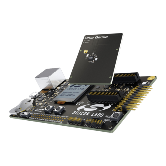
Silicon Laboratories EFR32BG1 User Manual (36 pages)
2.4 GHz 8 dBm WLCSP Wireless Starter Kit
Brand:
Silicon Laboratories
| Category:
Motherboard
| Size: 1 MB
Table of Contents
Introduction
2
Radio Boards
2
Ordering Information
2
Getting Started
2
Hardware Overview
3
Hardware Layout
3
Block Diagram
4
Connectors
5
J-Link USB Connector
5
Ethernet Connector
5
Breakout Pads
6
Expansion Header
6
Expansion Header Pin-Out
7
Debug Connector
8
Simplicity Connector
9
Debug Adapter
10
Power Supply and Reset
11
Radio Board Power Selection
11
Board Controller Power
12
EFR32 Reset
12
Peripherals
13
Push Buttons and Leds
13
Memory LCD-TFT Display
14
Serial Flash
15
Si7021 Relative Humidity and Temperature Sensor
16
Virtual COM Port
17
Host Interfaces
18
Serial Configuration
18
Hardware Handshake
19
I 2 C I/O Expander
20
Communication
21
Register Map
21
Board Controller
23
Admin Console
23
Connecting
23
Built-In Help
23
Command Examples
24
Virtual UART
24
Advanced Energy Monitor
25
Introduction
25
Theory of Operation
25
AEM Accuracy and Performance
26
Usage
26
On-Board Debugger
27
Host Interfaces
27
USB Interface
27
Ethernet Interface
27
Serial Number Identification
27
Debug Modes
28
Debugging During Battery Operation
29
Kit Configuration and Upgrades
30
Firmware Upgrades
30
Schematics, Assembly Drawings and BOM
31
Kit Revision History
32
SLWRB4101B Revision History
32
Document Revision History
33
Advertisement
Related Products
Silicon Laboratories EFR32MG13
Silicon Laboratories EFR32MG12
Silicon Laboratories EFR32xG22
Silicon Laboratories Thunderboard EFR32BG22
Silicon Laboratories EFR32ZG14
Silicon Laboratories EFR32xG21B
Silicon Laboratories Thunderboard EFM8UB3
Silicon Laboratories Thunderboard EFM32GG12
Silicon Laboratories EFM8LB1-SLSTK2030A
Silicon Laboratories EFM8UB2-SLSTK2001A
Silicon Laboratories Categories
Motherboard
Microcontrollers
Computer Hardware
Control Unit
Adapter
More Silicon Laboratories Manuals
Login
Sign In
OR
Sign in with Facebook
Sign in with Google
Upload manual
Upload from disk
Upload from URL