Sign In
Upload
Manuals
Brands
S&T Manuals
Motherboard
Kontron 3.5"-SBC-KBL
S&T Kontron 3.5"-SBC-KBL Manuals
Manuals and User Guides for S&T Kontron 3.5"-SBC-KBL. We have
1
S&T Kontron 3.5"-SBC-KBL manual available for free PDF download: User Manual
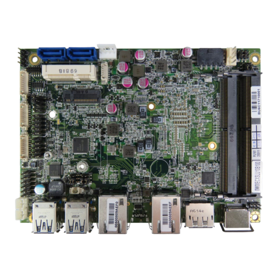
S&T Kontron 3.5"-SBC-KBL User Manual (77 pages)
Brand:
S&T
| Category:
Motherboard
| Size: 3 MB
Table of Contents
Symbols
7
For Your Safety
8
High Voltage Safety Instructions
8
Special Handling and Unpacking Instruction
8
Lithium Battery Precautions
9
General Instructions on Usage
9
Quality and Environmental Management
9
Disposal and Recycling
9
WEEE Compliance
9
Table of Contents
10
List of Tables
11
List of Figures
12
1/ Introduction
14
2/ Installation Procedures
15
2.1. Installing the Board
15
2.2. Chassis Safety Standards
16
2.3. Lithium Battery Replacement
16
3/ System Specifications
18
3.1. System Block Diagram
18
Figure 1: System Block Diagram 3.5"-SBC-KBL
18
3.2. Component Main Data
19
Table 1: Component Main Data
19
3.3. Environmental Conditions
20
3.4. Standards and Certifications
20
Table 2: Environmental Conditions
20
Table 3: Standards and Certifications
20
3.5. Processor Support
21
3.6. System Memory Support
21
Table 4: Processor Support
21
Memory Operating Frequencies
22
3.7. On-Board Graphics Subsystem
22
Table 5: Memory Operating Frequencies
22
3.8. Power Supply Voltage
23
Table 6: Three-Displays Configurations
23
Table 7: Supply Voltages
23
4/ Connector Locations
24
4.1. Top Side
24
Table 8: Jumper List
24
Table 9: Top Side Internal Connector Pin Assignment
24
Figure 2: Top Side
24
4.2. Rear Side
26
Table 10: Rear Side Internal Connector Pin Assignment
26
Figure 3: Rear Side
26
4.3. Connector Panel Side
27
Table 11: Connector Panel Side Connector List
27
Figure 4: Connector Panel Side
27
5/ Connector Definitions
28
6/ I/O-Area Connectors
29
HDMI Connector (HDMI1)
29
Table 12: Pin Assignment HDMI Connector HDMI1
29
Figure 5: HDMI Connector HDMI1
29
DP Connector (DP1)
30
Table 13: Pin Assignment DP Connector DP1
30
Figure 6: DP Connector DP1
30
Ethernet Connectors (CN11 & CN12)
31
Table 14: Pin Assignment Ethernet Connectors CN11, CN12
31
Figure 7: Ethernet Connectors CN11, CN12
31
USB Connectors (I/O Area)
32
Table 15: Pin Assignment USB3.0 Connectors CN13, CN14
32
Figure 8: USB 3.0 Connectors CN13, CN14
32
Table 16: Signal Description
33
Figure 9: USB 2.0 High Speed Cable
33
Figure 10: USB 3.0 High Speed Cable
33
7/ Internal Connectors
34
7.1. Power Connector
34
Power Input Wafer (CN2)
34
RTC Power Input Wafer (BAT1)
34
Table 17: Pin Assignment CN2
34
Table 18: Pin Assignment BAT1
34
Figure 11: Power Input Wafer CN2
34
Figure 12: RTC Power Input Wafer BAT1
34
Fan Wafer (FAN1)
35
Table 19: 4-Pin Mode FAN1
35
Table 20: 3-Pin Mode FAN1
35
Table 21: Signal Description
35
Figure 13: Fan Wafer FAN1
35
SATA (Serial ATA) Disk Interfaces (SATA1 & SATA2)
36
Table 22: Pin Assignment SATA1, SATA2
36
Table 23: Signal Description
36
Figure 14: SATA Connector SATA1, SATA2
36
HDD Power Output Wafer (CN1)
37
Table 24: Pin Assignment CN1
37
Figure 15: HDD Power Output Wafer CN1
37
USB Connectors (Internal) (CN8)
38
Table 25: Pin Assignment CN8
38
Table 26: Signal Description
38
Figure 16: USB 2.0 Pin Header CN8
38
Speaker Connector (CN10 & CN15)
39
Audio Connector (CN9)
39
Table 27: Pin Assignment CN8
39
Table 28: Pin Assignment CN8
39
Figure 17: 3W Audio AMP Output Wafer CN10 (Left Channel), CN15 (Right Channel)
39
Figure 18: Audio Input / Output Pin Header CN9
39
Front Panel Pin Header (FP1 & FP2)
40
Table 29: Pin Assignment FP1
40
Table 30: Signal Description
40
Figure 19: Front Panel Pin Header FP1
40
Figure 20: Front Panel Pin Header FP2
40
Table 31: Pin Assignment FP2
41
Table 32: Signal Description
41
Serial COM1 - COM2 Ports (CN6 & CN7)
42
Table 33: Pin Assignment CN6, CN7
42
Table 34: Signal Description
42
Figure 21: Serial COM CN6, CN7
42
LVDS Flat Panel Connector (LVDS1)
43
Table 35: Pin Assignment LVDS1
43
Figure 22: LVDS Connector LVDS1
43
Table 36: Signal Description
44
LCD Panel Power Connector for LVDS1 (CN16)
45
Table 37: Pin Assignment CN16
45
Table 38: Signal Description
45
Figure 23: LCD Panel Power Connector CN16
45
Digital Input / Output Wafer (CN5)
46
Table 39: Pin Assignment CN5
46
Table 40: Signal Description
46
Figure 24: Digital Input / Output Wafer CN5
46
Mpcie Slot Connector (MPCIE1)
47
Table 41: Pin Assignment MPCIE1
47
Figure 25: Mpcie Slot Connector MPCIE1
47
NGFF M.2 Key B Slot Connector (CON1)
49
Table 42: Pin Assignment CON1
49
Figure 26: NGFF M.2 Key B Slot Connector CON1
49
SIM Card Connector (CN4)
51
Table 43: Pin Assignment CN4
51
Figure 27: SIM Interface Wafer CN4
51
7.16. Switches and Jumpers
52
MPCIE1 Activity LED Pin Header (JP1)
52
Panel & Backlight Power Selection for LVDS1 (JP2)
52
Table 44: Pin Assignment JP1
52
Table 45: Pin Assignment JP1
52
Figure 28: Jumper Connector
52
Figure 29: MPCIE1 Activity LED Pin Header JP1
52
Figure 30: Panel & Backlight Power Selection for LVDS1 (JP2)
52
NGFF M.2 Activity LED Pin Header (JP3)
53
Backlight Power Enable Selection for LVDS1 (JP4)
53
AT / ATX Power Mode & NGFF Msata / Mpcie Selection (JP6)
53
Table 46: Pin Assignment JP3
53
Table 47: Pin Assignment JP4
53
Table 48: Pin Assignment JP6
53
Figure 31: NGFF M.2 Activity LED Pin Header (JP3)
53
Figure 32: Backlight Power Enable Selection for LVDS1 (JP4)
53
Figure 33: at / ATX Power Mode & NGFF Msata / Mpcie Selection (JP6)
53
SIM Card and USB Power Selection (JP7)
54
Flash Descriptor Security Override Selection (JP8)
54
Table 49: Pin Assignment JP7
54
Table 50: Pin Assignment JP8
54
Figure 34: SIM Card and USB Power Selection (JP7)
54
Figure 35: Flash Descriptor Security Override Selection (JP8)
54
RTC Reset Selection (JP9)
55
Clear ME Register (JP10)
55
Table 51: Pin Assignment JP9
55
Table 52: Pin Assignment JP10
55
Figure 36: RTC Reset Selection (JP9)
55
Figure 37: Clear ME Register (JP10)
55
8/ On-Board Connectors & Mating Connector Types
56
Table 53: On-Board Connectors & Mating Connector Types
56
9/ Bios
57
9.1. Starting the Uefi BIOS
57
Table 54: Font Size Table
57
9.2. Setup Menus
58
Main Setup Menu
58
Table 55: Main Setup Menu Sub-Screens and Functions
58
Figure 38: BIOS Main Menu Screen System Data and Time
59
Advanced Setup Menu
60
Figure 39: BIOS Advanced Menu
60
Figure 40: BIOS Advanced Menu - Display Configuration
61
Figure 41: BIOS Advanced Menu - Super IO Configuration
63
Figure 42: BIOS Advanced Menu - Super IO Configuration - Serial Port 1 Configuration
63
Figure 43: BIOS Advanced Menu - Super IO Configuration - Serial Port 2 Configuration
64
Figure 44: BIOS Advanced Menu - CPU Chipset Configuration
65
Figure 45: BIOS Advanced Menu - SATA Configuration
66
Figure 46: BIOS Advanced Menu - USB Configuration
67
Figure 47: BIOS Advanced Menu - DIO Configuration
68
Figure 48: BIOS Advanced Menu - H/W Monitor
69
Power Setup Menu
70
Figure 49: BIOS Power Setup Menu
70
Figure 50: BIOS Power Setup Menu - Watchdog Timer Configuration
71
Boot Setup Menu
72
Figure 51: BIOS Boot Setup Menu
72
Security Setup Menu
73
Figure 52: BIOS Boot Setup Menu
73
9.2.5.1. Remember the Password
74
Save & Exit Setup Menu
75
Figure 53: BIOS Boot Setup Menu
75
Appendix A: List of Acronyms
76
Table 56: List of Acronym
76
About Kontron
77
Advertisement
Advertisement
Related Products
S&T Kontron pITX-iMX8M
S&T Kontron QDS-6100
S&T Kontron QDS-6200
S&T Kontron mITX-KBL-S-C236
S&T Kontron Mini ITX Skylake S/C236
S&T Kontron SBC-KBL-3965U-wTPM
S&T Kontron SBC-KBL-3965U-woTPM
S&T Kontron SBC-KBL-7100U
S&T Kontron SBC-KBL-7300U
S&T Kontron SBC-KBL-7300U-ET
S&T Categories
Computer Hardware
Switch
Desktop
Motherboard
Single board computers
More S&T Manuals
Login
Sign In
OR
Sign in with Facebook
Sign in with Google
Upload manual
Upload from disk
Upload from URL