Sign In
Upload
Manuals
Brands
Kontron Manuals
Single board computers
SBC-APL V2.0
Kontron SBC-APL V2.0 Manuals
Manuals and User Guides for Kontron SBC-APL V2.0. We have
1
Kontron SBC-APL V2.0 manual available for free PDF download: User Manual
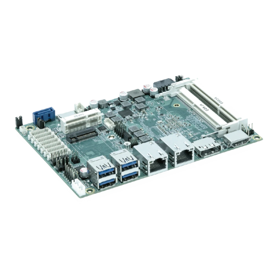
Kontron SBC-APL V2.0 User Manual (83 pages)
Brand:
Kontron
| Category:
Single board computers
| Size: 1 MB
Table of Contents
Symbols
6
For Your Safety
7
High Voltage Safety Instructions
7
Special Handling and Unpacking Instruction
7
Lithium Battery Precautions
8
General Instructions on Usage
8
Quality and Environmental Management
8
Disposal and Recycling
8
WEEE Compliance
8
Table of Contents
9
List of Tables
10
List of Figures
11
1/ Introduction
13
2/ Installation Procedures
14
Installing the Board
14
Chassis Safety Standards
15
Lithium Battery Replacement
15
3/ System Specifications
17
System Block Diagram
17
Figure 1: System Block Diagram 3.5"-SBC-APL V2.0
17
Component Main Data
18
Table 1: Component Main Data
18
Environmental Conditions
19
Standards and Certifications
19
Table 2: Environmental Conditions
19
Table 3: Standards and Certifications
19
Processor Support
20
System Memory Support
20
Memory Operating Frequencies
20
Table 4: Processor Support
20
On-Board Graphics Subsystem
21
Power Supply
21
Table 5: Memory Operating Frequencies
21
Table 6: Three-Displays Configurations
21
Table 7: Supply Voltages
21
4/ Connector Locations
22
Top Side
22
Table 8: Jumper List
22
Table 9: Top Side Internal Connector Pin Assignment
22
Figure 2: Top Side
22
Rear Side
24
Table 10: Rear Side Internal Connector Pin Assignment
24
Figure 3: Rear Side
24
Connector Panel Side
25
Table 11: Connector Panel Side Connector List
25
Figure 4: Connector Panel Side
25
5/ Connector Definitions
26
6/ I/O-Area Connectors
27
HDMI Connector (CN15)
27
Table 12: Pin Assignment HDMI Connector CN15
27
Figure 5: HDMI Connector CN15
27
DP Connector (CN13)
28
Table 13: Pin Assignment DP Connector CN13
28
Figure 6: DP Connector CN13
28
Ethernet Connectors (CN9 & CN10)
29
Table 14: Pin Assignment Ethernet Connectors CN9, CN10
29
Figure 7: Ethernet Connectors CN9, CN10
29
USB Connectors (I/O Area)
30
Table 15: Pin Assignment USB3.0 / USB2.0 Connector CN4, CN5
30
Figure 8: USB 3.0 Connector CN4, CN5
30
Table 16: Signal Description
31
Figure 9: USB 2.0 High Speed Cable
31
Figure 10: USB 3.0 High Speed Cable
31
7/ Internal Connectors
32
Power Connector
32
Power Input Wafer (CN1)
32
CR2032 Battery Power Input Wafer (BAT1)
32
Table 17: Pin Assignment CN1
32
Table 18: Pin Assignment BAT1
32
Figure 11: Power Input Wafer CN1
32
Figure 12: CR2032 Battery Power Input Wafer BAT1
32
DC5V Fan Wafer (FAN1)
33
Table 19: Pin Assignment FAN1
33
Table 20: Signal Description
33
Figure 13: DC5V Fan Wafer FAN1
33
SATA (Serial ATA) Port 0 Connector (SATA1)
34
Table 21: Pin Assignment SATA1
34
Table 22: Signal Description
34
Figure 14: SATA Port 0 Connector SATA1
34
HDD Power Output Wafer (CN2)
35
Table 23: Pin Assignment CN2
35
Figure 15: HDD Power Output Wafer CN2
35
USB Connectors (Internal) (CN6, CN26 Optional)
36
Table 24: Pin Assignment CN6
36
Table 25: Pin Assignment CN26 (Optional)
36
Table 26: Signal Description
36
Figure 16: USB 2.0 Port DN_1, DN_2 Pin Header CN6
36
Figure 17: USB 2.0 Port Wafer CN26 (Optional)
36
Audio AMP Output Wafer (CN12 & CN16)
38
Audio Input / Output Pin Header (CN11)
38
Table 27: Pin Assignment CN12, CN16
38
Table 28: Pin Assignment CN8
38
Figure 18: 3W Audio AMP Output Wafer CN12 (Left Channel), CN16 (Right Channel)
38
Figure 19: Audio Input / Output Pin Header CN11
38
Front Panel Pin Header (FP1 & FP2)
39
Table 29: Pin Assignment FP1
39
Table 30: Signal Description
39
Figure 20: Front Panel 1 Pin Header FP1
39
Figure 21: Front Panel 2 Pin Header FP2
39
Table 31: Pin Assignment FP2
40
Table 32: Signal Description
40
Serial COM1 - COM6 Ports (CN17 - CN22)
41
Table 33: Pin Assignment CN17, CN18
41
Table 34: Pin Assignment CN19 - CN22
41
Table 35: Signal Description
41
Figure 22: Serial COM CN17 - CN22
41
LVDS Panel Connector (LVDS1)
42
Table 36: Pin Assignment LVDS1
42
Figure 23: LVDS Connector LVDS1
42
Table 37: Signal Description
43
Backlight Power Output Wafer (CN23)
44
Table 38: Pin Assignment CN23
44
Table 39: Signal Description
44
Figure 24: Backlight Power Output Wafer CN23
44
Digital Input / Output Wafer (CN14)
45
Table 40: Pin Assignment CN14
45
Figure 25: Digital Input / Output Wafer CN14
45
Mpcie Socket (MPCIE1)
46
Table 41: Pin Assignment MPCIE1
46
Figure 26: Mpcie Slot Connector MPCIE1
46
NGFF M.2 Key B Socket (CON1)
48
Table 42: Pin Assignment CON1
48
Figure 27: NGFF M.2 Key B Slot Connector CON1
48
SIM Interface Wafer for MPCIE1 and M.2 Key B (CN7)
51
Table 43: Pin Assignment CN7
51
Figure 28: SIM Interface Wafer CN7
51
Micro-SD Card Cage (CN3)
52
Table 44: Pin Assignment CN3
52
Figure 29: Micro-SD Card Cage CN3
52
Switches and Jumpers
53
SIM Card Selection (JP1)
53
Backlight Enable Selection (JP2)
53
Table 45: Pin Assignment JP1
53
Figure 30: Jumper Connector
53
Figure 31: SIM Card Selection (JP1)
53
Figure 32: Backlight Enable Selection JP2
53
Panel & Backlight Power Selection (JP3)
54
AT / ATX Power Mode Selection (JP4)
54
Table 46: Pin Assignment JP2
54
Table 47: Pin Assignment JP3
54
Figure 33: Panel & Backlight Power Selection JP3
54
Figure 34: at / ATX Power Mode Selection JP4
54
Key B Activity LED Pin Header (JP5)
55
MPCIE Activity LED Pin Header (JP6)
55
RTC Reset Selection (JP8)
55
Table 48: Pin Assignment JP4
55
Table 49: Pin Assignment JP5
55
Table 50: Pin Assignment JP6
55
Figure 35: M.2 Key B Activity LED Pin Header JP5
55
Figure 36: MPCIE1 Activity LED Indication JP6
55
USB Power Selection (JP9)
56
ME F/W Selection (JP10)
56
Table 51: Pin Assignment JP8
56
Table 52: Pin Assignment JP9
56
Figure 37: RTC Reset Selection JP8
56
Figure 38: USB Power Selection JP9
56
Figure 39: ME F/W Selection JP10
56
Table 53: Pin Assignment JP10
57
8/ On-Board Connectors & Mating Connector Types
58
Table 54: On-Board Connectors & Mating Connector Types
58
9/ Bios
59
Starting the Uefi BIOS
59
Table 55: Font Size Table
59
Setup Menus
60
Main Setup Menu
60
Table 56: Main Setup Menu Sub-Screens and Functions
60
Figure 40: BIOS Main Menu Screen System Data and Time
61
Advanced Setup Menu
62
Figure 41: BIOS Advanced Menu
63
Figure 42: BIOS Advanced Menu - Display Configuration
64
Figure 43: BIOS Advanced Menu - Super IO Configuration
65
Figure 44: BIOS Advanced Menu - Super IO Configuration - Serial Port 1 Configuration
65
Figure 45: BIOS Advanced Menu - Super IO Configuration - Serial Port 2 Configuration
66
Figure 46: BIOS Advanced Menu - Super IO Configuration - Serial Port 3 Configuration
67
Figure 47: BIOS Advanced Menu - Super IO Configuration - Serial Port 4 Configuration
67
Figure 48: BIOS Advanced Menu - Super IO Configuration - Serial Port 5 Configuration
68
Figure 49: BIOS Advanced Menu - Super IO Configuration - Serial Port 6 Configuration
69
Figure 50: BIOS Advanced Menu - CPU Chipset Configuration
70
Figure 51: BIOS Advanced Menu - SATA Configuration
71
Figure 52: BIOS Advanced Menu - USB Configuration
72
Figure 53: BIOS Advanced Menu - DIO Configuration
73
Figure 54: BIOS Advanced Menu - Network Stack
74
Figure 55: BIOS Advanced Menu - H/W Monitor
75
Power Setup Menu
76
Figure 56: BIOS Power Setup Menu
76
Figure 57: BIOS Power Setup Menu - Watchdog Timer Configuration
77
Boot Setup Menu
78
Figure 58: BIOS Boot Setup Menu
78
Security Setup Menu
79
Figure 59: BIOS Boot Setup Menu
79
Remember the Password
80
Save & Exit Setup Menu
81
Figure 60: BIOS Boot Setup Menu
81
Appendix A: List of Acronyms
82
Table 57: List of Acronyms
82
About Kontron
83
Advertisement
Advertisement
Related Products
Kontron VX3230
Kontron KISS 1U Short V2 KTQM87-A
Kontron KISS 2U V2 KTQ87-A
Kontron KISS 2U V2 PCI762-A
Kontron VX3905
Kontron KISS 2U V3 PCI763
Kontron V Panel Express Series
Kontron Easy VM6050
Kontron VM6250-WA
Kontron VM6250-RC
Kontron Categories
Computer Hardware
Motherboard
Server
Industrial PC
Desktop
More Kontron Manuals
Login
Sign In
OR
Sign in with Facebook
Sign in with Google
Upload manual
Upload from disk
Upload from URL