Sign In
Upload
Manuals
Brands
Beck Manuals
Controller
IPC SC123-IEC
Beck IPC SC123-IEC Manuals
Manuals and User Guides for Beck IPC SC123-IEC. We have
1
Beck IPC SC123-IEC manual available for free PDF download: Hardware Manual
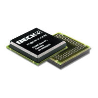
Beck IPC SC123-IEC Hardware Manual (61 pages)
CHIP Embedded Controller
Brand:
Beck
| Category:
Controller
| Size: 1 MB
Table of Contents
Table of Contents
3
Overview
7
Features
8
Block Diagram
9
Figure 3-1: Block Diagram
9
Pin Description
10
Pin Configuration
10
Figure 4-1: Ball Grid Array Looking through Top of Package
10
System Interface
11
Table 4-1: Pin Description of System Interface
12
Chip Selects
13
Table 4-2: Pin Description of Chip Selects
13
Dma
14
Interrupts
14
UART0 Interface
14
Table 4-3: Pin Description of DMA Request Pins
14
Table 4-4: Pin Description of Interrupts
14
Table 4-5: Pin Description of UART0
14
UART1 Interface
15
UART2 Interface
15
Table 4-6: Pin Description of UART1
15
Table 4-7: Pin Description of UART2
15
I²C Bus
16
Pure Pios
16
Table 4-8: Pin Description of I²C Bus
16
Table 4-9: Pin Description of Pure PIO Pins
16
SPI Bus / UART3
17
Timers
17
Table 4-10: Pin Description of SPI Bus / UART3
17
Table 4-11: Pin Description of Timers
17
CAN Bus Interface
18
USB Interface
18
JTAG Interface
18
Table 4-12: Pin Description of CAN Bus
18
Table 4-13: Pin Description of USB
18
Table 4-14: Pin Description of JTAG
18
Ethernet 0 Interface (Internal PHY)
19
MII Ethernet 1 Interface (External PHY)
19
Table 4-15: Pin Description of Internal PHY
19
Table 4-16: Pin Description of MII
19
PHY Power (Internal PHY)
20
Power
20
Table 4-17: Pin Description of PHY Power Pins
20
Table 4-18: Pin Description of Power Pins
20
Programmable I/O Pins
21
Table 4-19: List of PIO Sharing Designations
21
System Start-Up Configuration
22
PIO Pins
22
Address Pins
22
PFI Pin
23
Figure 5-1: Power on Flowchart with Power Fail Interrupt Enabled
23
Functional Description
24
Cpu
24
Registers
24
Table 6-1: General Purpose Registers
24
Table 6-2: Segment, Status and Control Registers
24
Memory Organization
25
24-Bit Address Mode
25
Figure 6-1: 24-Bit Address Generation
25
Figure 6-2: Contiguously Segments in Memory
25
Table 6-3: Segment Register Selection Rules
25
Peripheral Accesses through the Address-/Databus
26
Figure 6-3: 8 Bit Read Access from C00 , CSBE = 0, Read = 0X55
26
Figure 6-4: 16 Bit Read Access from C00 , CSBE = 0, Read = 0X1234
26
Figure 6-5: 16 Bit Read Access from C01 , CSBE = 0, Read = 0X5678
27
Figure 6-6: 8 Bit Read Access from C01 , CSBE = 0, Read = 0X55
27
Figure 6-7: 8 Bit Write Access to C00 , CSBE = 0, Write = 0X23
28
Figure 6-8: 16 Bit Write Access to C00 , CSBE = 0, Write = 0X1234
28
Figure 6-9: 16 Bit Write Access to C01 , CSBE = 0, Write = 0X5678
29
Figure 6-10: 8 Bit Write Access to C01 , CSBE = 0, Write = 0X23
29
Figure 6-11: 8 Bit Write Access to C00 , CSBE = 1, Write = 0X23
30
Figure 6-12: 8 Bit Write Access to C01 , CSBE = 1, Write = 0X23
30
Figure 6-13: 16 Bit Write Access to C00 , CSBE = 1, Write = 0X1234
31
Figure 6-14: 16 Bit Write Access to C01 , CSBE = 1, Write = 0X5678
31
Uarts
32
RTOS Update Via Serial Ports
32
Spi
33
Table 6-4:Context between SDO and SDI to MOSI and MISO in Different Modes
34
Can
36
Introduction
36
Table 6-5: Provided CAN Baud Rates
36
TX Channels
37
RX Channel
37
Figure 6-15: TX Message Routing
37
Usb
38
Figure 6-16: Pullup-/Down Resistors for USB Full-Speed Device
38
Power Fail Interrupt
39
Description
39
Storing Non-Volatile Data to Internal Flash Memory
39
Storing Non-Volatile Data to External Memory
39
Mapping External Memory
40
MII Interface
40
Figure 6-17: Sketch of the Logic to Decode the Chip Select for an External Memory
40
Table 6-6: Truth Table of FLSSEL and UCSOUT# and External Memory
40
Timers
41
Reset
41
Figure 6-18: Internal Reset Processing
41
System Overview
42
Memory Map
42
Figure 7-1: Memory Map
42
System Interrupts
43
Watchdog
43
Characteristics
44
Absolute Maximum Ratings
44
Recommended Operating Ranges
44
Voltage and Temperature
44
Supply Current
44
Table 8-1: Absolute Maximum Ratings
44
Table 8-2: Recommended Operating Ranges
44
Table 8-3: Supply Current
44
Inputs
45
Outputs
45
Programmable Input/Output Pins
45
XIN/XOUT Pins
45
Table 8-4: Inputs
45
Table 8-5: Outputs
45
Table 8-6: Pios
45
Table 8-7: 3. I/O Characteristics Xin/Xout Pins
45
PHY Receiver Input Characteristics
46
100Base-TX Transceiver Characteristics
46
Table 8-8: PHY Receiver Input Characteristics
46
Table 8-9: 100Base-TX Transceiver Characteristics
46
AC Characteristics
47
Timing Parameter List
47
Table 8-10: AC Characteristics
47
System Bus Timing
48
Figure 8-1: System Bus Timing
48
Reset Timing
49
Figure 8-2: Reset Timing
49
Routing and Placement Rules
50
PCB Board Design Suggestion for SC123/SC143
50
Figure 9-1: PCB Board Design Suggestion
50
Figure 9-2: PCB Board Design Suggestion
50
Routing and Placement Rules for Ethernet Components
51
Suggested Magnetics
51
Package Information
52
Dimensions
52
Figure 10-1: Package Dimensions
52
Table 10-1: Package Dimensions
52
Cover Description
53
Figure 10-2: Cover
53
Application Examples
54
Minimum Circuit Requirements
54
Figure 11-1: Minimum Circuit Requirements for Sc1X3
54
Ethernet Example Circuit
55
Figure 11-2: Ethernet Example Circuit 1
55
External Memory
56
Figure 11-3: Example Circuit for Connecting an External Memory
56
Traffic/Link/Speed Leds
57
Figure 11-4: Circuit Example for Two Bi-Coloured Leds
57
Figure 11-5: Circuit Example for Four Mono-Coloured Leds
57
Sc1X3 Socket
58
Custom Series Programming of Sc1X3
58
Figure 11-6: Sc1X3-Socket
58
CPUCLK Handling
59
Reflow Profile
60
Figure 13-1: Reflow Profile
60
Table 13-1: Typical Reflow Profile Conditions
60
History
61
Advertisement
Advertisement
Related Products
Beck IPC SC123-LF
Beck IPC SC123-IEC-LF
Beck IPC SC143-LF
Beck IPC SC143-IEC
Beck IPC SC143-IEC-LF
Beck IPC@CHIP Series
Beck IPC@CHIP DK41
Beck IPC@CHIP DK51
Beck IPC@CHIP DK55
Beck IPC SC123
Beck Categories
Controller
Transducer
Switch
Network Hardware
Industrial Equipment
More Beck Manuals
Login
Sign In
OR
Sign in with Facebook
Sign in with Google
Upload manual
Upload from disk
Upload from URL