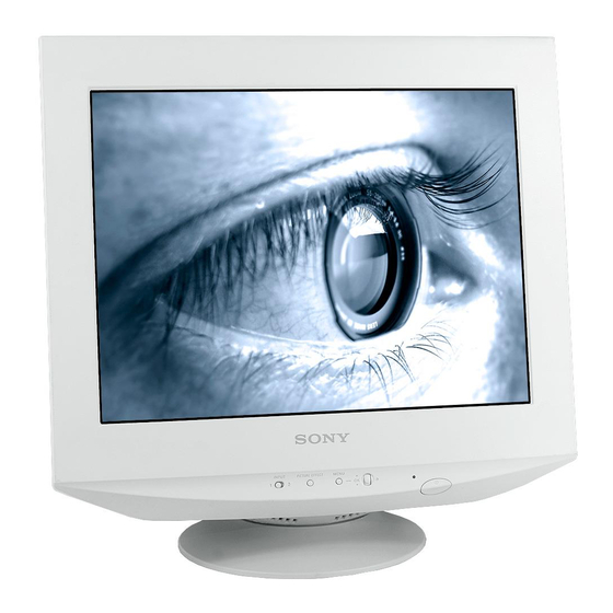
Sony TRINITRON CPD-G500 Service Manual
Color computer display
Hide thumbs
Also See for TRINITRON CPD-G500:
- Operating instructions manual (76 pages) ,
- Specifications (2 pages) ,
- Brochure & specs (14 pages)
Table of Contents
Advertisement
SERVICE MANUAL
CRT
Viewable image size
Resolution
Maximum
Recommended
Standard image area
SPECIFICATIONS
0.24 mm aperture grille pitch
21 inches measured diagonally
90-degree deflection
FD Trinitron
Approx. 403.8 × 302.2 mm (w/h)
(16 × 12 inches)
19.8" viewing image
Horizontal: 2048 dots
Vertical: 1536 lines
Horizontal: 1600 dots
Vertical: 1200 lines
Approx. 388 × 291 mm (w/h)
× 11
3
1
(15
/
/
inches)
8
2
or
Approx. 364 × 291 mm (w/h)
× 11
3
1
(14
/
/
inches)
8
2
TRINITRON
CPD-G500
Canadian Model
S.Hemisphere Model
Deflection frequency*
AC input voltage/current 100 to 240 V, 50 – 60 Hz, 2.0 – 1.0 A
Power consumption
Dimensions
Mass
Plug and Play
* Recommended horizontal and vertical timing condition
• Horizontal sync width duty should be more than 4.8% of total
horizontal time or 0.8 µs, whichever is larger.
• Horizontal blanking width should be more than 2.3 µsec.
• Vertical blanking width should be more than 450 µsec.
** If the input signal is Generalized Timing Formula (GTF)
compliant, the GTF feature of the monitor will automatically
provide an optimal image for the screen.
Design and specifications are subject to change without notice.
COLOR COMPUTER DISPLAY
®
US Model
AEP Model
Chassis No. SCC-L22C-A
Chassis No. SCC-L22G-A
Equator Model
Chassis No. SCC-L22F-A
G1
CHASSIS
Horizontal: 30 to 121 kHz
Vertical: 48 to 160 Hz
Approx. 145 W
Approx. 497 × 480 × 478 mm (w/h/d)
× 19 × 18
5
7
(19
/
/
inches)
8
8
Approx. 32 kg (70 lb 9 oz)
DDC1/2B/2Bi, GTF**
Advertisement
Table of Contents

Related Manuals for Sony TRINITRON CPD-G500


Summary of Contents for Sony TRINITRON CPD-G500
-
Page 1: Service Manual
CPD-G500 SERVICE MANUAL US Model Canadian Model AEP Model Chassis No. SCC-L22C-A S.Hemisphere Model Chassis No. SCC-L22G-A Equator Model Chassis No. SCC-L22F-A CHASSIS SPECIFICATIONS 0.24 mm aperture grille pitch Deflection frequency* Horizontal: 30 to 121 kHz 21 inches measured diagonally Vertical: 48 to 160 Hz 90-degree deflection AC input voltage/current 100 to 240 V, 50 –... - Page 2 VIEWS AND IN THE PARTS LIST ARE CRITICAL FOR Parts on Set SAFE OPERATION. REPLACE THESE COMPONENTS WITH SONY PARTS WHOSE PART NUMBERS AP- PEAR AS SHOWN IN THIS MANUAL OR IN SUPPLE- MENTS PUBLISHED BY SONY. CIRCUIT ADJUST- MENTS THAT ARE CRITICAL FOR SAFE OPERATION 0.15 µ...
-
Page 3: Power Saving Function
1 (power) indicator and inform your authorized connectors, or turn off the connected computer(s). Sony dealer of the monitor’s condition. Be sure to note the model name and serial number of your monitor. Also note the make and Press the 1 (power) button twice to turn the monitor model of your computer and video board. -
Page 4: Timing Specification
CPD-G500 TIMING SPECIFICATION MODE AT PRODUCTION MODE 1 MODE 2 MODE 3 MODE 4 RESOLUTION 1600 X 1200 1920 X 1440 1800 X 1440 1800 X 1350 CLOCK 229.500 MHz 297.000 MHz 299.436 MHz 300.000 MHz — HORIZONTAL — H-FREQ 106.250 kHz 112.500 kHz 120.740 kHz... -
Page 5: Table Of Contents
CPD-G500 TABLE OF CONTENTS Section Title Page 1. GENERAL ..............1-1 2. DISASSEMBLY 2-1. Cabinet Removal ..........2-1 2-2. D Board Removal ..........2-1 2-3. G Board Removal ..........2-2 2-4. A Board, I/O Terminal Board Assembly Removal ............. 2-2 2-5. -
Page 6: General
SECTION 1 The operating instructions mentioned here are partial abstracts from the Operating Instruction Manual. The page numbers of GENERAL the Operating Instruction Manual remain as in the manual. Use of the tilt-swivel Precautions Identifying parts and controls This monitor can be adjusted within the angles shown below. To find the center of the monitor’s turning radius, align the center of Warning on power connections See the pages in parentheses for further details. - Page 7 If no picture appears on your screen x Connecting to a Macintosh or compatible Step 2: Connect the power cord Setup • Check that the monitor is correctly connected to the computer. computer • If NO INPUT SIGNAL appears on the screen, try changing the With the monitor and computer switched off, first connect the input signal (page 8), and confirm that your computer’s graphic power cord to the monitor, then connect it to a power outlet.
- Page 8 6 CONV (page 12) Selecting the on-screen menu Selecting the input signal CONVERGENCE Customizing Your Monitor Select the CONV menu to adjust the language (LANG) picture’s horizontal and vertical You can connect two computers to this monitor using the HD15 convergence.
- Page 9 x Using the control button Adjusting the brightness and Automatically sizing and centering Adjusting the centering of the contrast the picture (AUTO) picture (CENTER) Display the main MENU. Press the center of the control button to display the main MENU on your screen. Brightness and contrast adjustments are made using a separate You can easily adjust the picture to fill the screen by using the This setting is stored in memory for the current input signal.
- Page 10 Adjusting the shape of the picture Adjusting the convergence (CONV) Adjusting the quality of the picture Adjusting the color of the picture (GEOM) (SCREEN) (COLOR) The CONV settings allow you to adjust the quality of the picture by controlling the convergence. The convergence refers to the The GEOM settings allow you to adjust the rotation and shape of The SCREEN settings allow you to adjust the quality of the The COLOR settings allow you to adjust the picture’s color...
- Page 11 Restoring the color from the EASY or sRGB menus EXPERT mode Setting the color temperature for each of the Additional settings (OPTION) video input connectors The colors of most display monitors tend to gradually lose brilliance You can make additional adjustments to the color in greater detail over several years of service.
-
Page 12: Troubleshooting
If OUT OF SCAN RANGE appears on the screen Resetting the adjustments Troubleshooting Technical Features I NFORMA T I ON MON I TOR I S WORK I NG This monitor has the following three reset methods. Use the : 1 3 0 . 0 k H z / Before contacting technical support, refer to this section. - Page 13 Install the Windows Monitor Information Disk (page 7) and select this monitor of the picture tube. (“CPD-G500/G500J”) from among the Sony monitors in the Windows 95/98 monitor I MAGE selection screen. If you choose to select “Plug and Play,” connect the monitor to the...
-
Page 14: Specifications
Count the number of seconds between orange flashes of the 1 (power) indicator and inform your authorized Sony dealer of the monitor’s condition. Be sure to note the model name and serial number of your monitor. Also note the make and... -
Page 15: Disassembly
CPD-G500 SECTION 2 DISASSEMBLY 2-1. CABINET REMOVAL Push in the tip of a screwdriver about 5mm to unlock the claw. Cabinet Cabinet Two claws Four screws Bezel assembly Bezel assembly (+ BVTT 4 x 8) Cabinet Top cover Two screws (+ BVTP 4 x 16) Two claws Three screws... -
Page 16: G Board Removal
CPD-G500 2-3. G BOARD REMOVAL Four screws (+BVTP 3 x 8) G shield Three screws (+ BVTT 4 x 8) CN602 G board CN654 CN653 CN652 CN650 Two screws (+ BVTP 3 x 8) AC inlet (3P) Two hooks Open the G block in the direction of the arrow . -
Page 17: N Board Removal
CPD-G500 2-5. N BOARD REMOVAL CN5003 CN5002 CN001 CN5001 CN002 CN007 CN010 CN011 N board Printed circuit board holder 2-6. SERVICE POSITION CAUTION : SHORT D,G boards Rear shield If the claw is hooked, opening and closing the board is impossible. Do not try to do it by force. -
Page 18: Bezel Assembly, H1 Board Removal
CPD-G500 2-7. BEZEL ASSEMBLY, H1 BOARD REMOVAL Before removing the bezel assembly, secure the picture tube by attaching two screws to the picture tube shield at the positions shown with an arrow (diagonal two places) Four screws to prevent the picture tube from falling. (Use (Tapping screw 5) the screws +BVTT 4 x 8 that fix top cover.) Picture tube shield... -
Page 19: J Board Removal
CPD-G500 2-9. J BOARD REMOVAL Two screws (+BVTT 4 x 8) Remove the picture tube. (Refer to 2-8.) 4pin 2pin CN601 4pin J board CN891 Picture tube shield complete assembly. Two hooks Claw • REMOVAL OF ANODE-CAP NOTE: Short circuit the anode of the picture tube and the anode cap to the metal chassis, CRT shield or carbon painted on the CRT, after removing the anode. -
Page 20: Harness Location
CPD-G500 2-10. HARNESS LOCATION H1 board J board Picture tube CN801 4pin 4pin CN651 CN601 CN650 CN603 CN5001 CN508 CN505 CN509 CN652 CN5003 CN502 CN002 CN5002 CN653 CN602 CN654 CN001 CN506 CN501 AC inlet G board D board N board Rear shield I/O terminal board assembly CN402... -
Page 21: Safety Related Adjustment
CPD-G500 SECTION 3 SAFETY RELATED ADJUSTMENT When replacing or repairing the shown below table, the c) Beam Current Protector Circuit Check following operational checks must be performed as a (1st Protector): D Board safety precaution against X-rays emissions from the unit. 1) Apply 4.5 V DC to CN504 0 pin on the D board, and check high voltage value. -
Page 22: Adjustments
CPD-G500 SECTION 4 ADJUSTMENTS Note: Hand degauss must be used on stand-by or power-off condition. This model has an automatic earth magnetism correction function by using an earth magnetism sensor and a LCC coil. When using a hand degauss while monitor (LCC coil) is being operated, it sometimes gets magnetized, and the system may not work properly as a result. - Page 23 CPD-G500 Connect the communication cable of the computer to the connector located on the D board. Run the service software and then follow the instruction. 1-690-391-21 A-1500-819-A 3-702-691-01 Interface Unit Connector Attachment IBM AT Computer To BUS CONNECTOR as a Jig D-sub mini Din 4 Pin...
- Page 24 CPD-G500 MEMO...
-
Page 25: Diagrams
SECTION 5 DIAGRAMS 5-1. BLOCK DIAGRAMS CN402 BIN2 GIN2 RIN2 IC401 IC402 IC403 INPUT SELECT RGB AMP RGB DRIVE CN407 CN408 CN401 V901 BIN2 ROUT ROUT ROUT HD15 PICTURE TUBE GIN2 RIN2 GOUT GOUT GOUT HEATER+ HEATER+ BOUT BOUT BOUT BIN1 INPUT1(HD15) GIN1... - Page 26 µ-COM, V.CONV, H. CONV, LCC, GEO MAGNETIC SENSOR IC5301 (2/2) CN5002 LCC-LB (+) – LCC-LB IC001 LCC-LB (–) CPU/DSP CN002 LCC-LT (+) IC5301 (1/2) LCC-LT LCC-LT (–) HS/CS 2 UIN3 VS 2 UIN4 LCC-RB (+) – IC011 LCC-RB LCC-RB (–) TO CONNECTOR HOST GND 2 P54/INT4...
- Page 27 (POWER SUPPLY) CN654 IC650 H CENT H +220V SHUNT REG S891 H CENT N POWER T620 CN891 TH601 CN603 H CENT L D650 AC L OUT AC L OUT +220V TO D BOARD AC L IN AC L IN +220V CN508 D610 (POWER SW)
-
Page 28: Frame Shcematic Diagram
5-2. FRAME SCHEMATIC DIAGRAM CN401 INPUT1(HD15) HD15D-SUB VIDEO AMP, CN407 CN408 RGB OUT CN402 CONNECTOR PANEL :S-MICRO B GND 2 B IN 2 G GND 2 PICTURE G IN 2 R GND 2 HEATER+ HEATER+ TUBE R IN 2 C BLOCK (CRT SOCKET) 5BNC INPUT2(BNC) -
Page 29: Circuit Boards Location
5-4. SCHEMATIC DIAGRAMS AND PRINTED 5-3. CIRCUIT BOARDS LOCATION Terminal name of semiconductors in silk screen Part Replaced ([) WIRING BOARDS printed circuit ( HV ADJ RV901 Note: Circuit Device Printed symbol Terminal name • All capacitors are in µF unless otherwise noted. (pF: µµF) Collector Capacitors without voltage indication are all 50 V. -
Page 30: Schematic Diagram Of A Board
(1) Schematic Diagram of A Board IC403 FA4301 5V-2 +12V IC401 C BLOCK IC402 RGB AMP M52757FP-TP M52749FP-TP R338 D101 INPUT SELECT RGB DRIVE R116 1PS226-115 C107 :CHIP 4.7k C101 C411 :CHIP R112 CN402 0.01 R_IN2 VCC2 OSD_BLK VCC2 R337 B:CHIP R105 (GND) - Page 31 • A BOARD IC401 M52757FP CONNECTOR PANEL TO A BOARD V901 CN402 PICTURE TUBE 21TKC Sync Sepa TO D BOARD T902(FBT)HV 5BNC INPUT2(BNC) B-SS3484<J..>-A..-P2-EPS05 TO N BOARD CN002 • A BOARD IC402 M52749FP • A BOARD WAVEFORMS OSD IN (R) MAIN RETRACE INPUT (R)
- Page 32 VIDEO AMP RGB OUT — A BOARD (Conductor Side) — • A BOARD — A BOARD (Component Side) — SEMICONDUCTOR LOCATION Conductor Component Side Side IC401 IC402 IC403 IC404 IC405 IC406 IC407 TRANSISTOR Conductor Component Side Side Q101 Q201 Q301 Q401 !∞...
-
Page 33: Schematic Diagrams Of H1, J Boards
USER CONTROL POWER SW (2) Schematic Diagrams of H1, J Boards — J BOARD — Q803 1W+5V 2SA1309A LED DRIVE CN891 R813 S891 C802 POWER Q804 AC L OUT 2SA1309A R823 Q801 LED DRIVE R824 2SC3311A STBY+5V CN801 AC L IN 1.5k LED DRIVE TO G BOARD... -
Page 34: Schematic Diagram Of D Board
(3) Schematic Diagram of D Board TO A BOARD CN406 TO CHASSIS TO G BOARD CN654 CN506 CN508 CN507 :S-MICRO D922 ERA34-10TP1 R901 D901 100k 1SS133T-77 :CHIP R549 400V 0.47 R560 IC502 R574 C552 CN501 R553 C909 C910 R903 D908 R917 1/2W LA6500-FA... - Page 35 DEFLECTION • D BOARD WAVEFORMS — D BOARD — 8.8 Vp-p (H) 1.9 Vp-p (H) 568 Vp-p (H) 50.6 Vp-p (H) 54.5 Vp-p (H) 2.1 Vp-p (H) • D BOARD SEMICONDUCTOR LOCATION DIODE IC501 IC502 D504 IC503 D505 IC701 D506 IC901 D507 D508...
-
Page 36: Schematic Diagrams Of N (A, B, C) Board
• Divided circuit diagram One sheet of N board circuit diagram is divided into three sheets, a b 1 each having the code N-a to N-c. For example, the destination Ref. No. (4) Schematic Diagrams of N (a, b, c) Board ab1 on the code N-a sheet is connected to ab1 on the N-b sheet. - Page 37 (µ-COM,GEO MAGNETIC SENSOR) STBY+5V IC006 TL082CPS-E20 ABL DET AMP GND10 AIN4 UPWM5 AVSS2 GND11 AIN3 MOIRECONT UPWM6 AIN2 KEYDET VDD9 AIN1 HSHPBAL TEMP UPWM7 AIN0 VDD10 AVDD1 UPWM8 DAC1 GND12 AVSS1 HDF0 GND13 DAC0 Q010 VCONV UPWM9 GND4 2SA1037AK INPUTSEL INV.
- Page 38 STBY+5V -15V +15V IC5401 IC5101 IC5301 IC5201 +15V LA6515 LA6515 LA6515 LA6515 V.S1 V.S1 V.S1 V.S1 OUT1 V.S2 OUT1 V.S2 OUT1 V.S2 OUT1 V.S2 OUT2 OUT2 OUT2 OUT2 -15V (H.V.CONV,LCC) B-SS9116<NH.>-N..-P3-EPS05 CN5001 CN5003 CN5002 :S-MICRO :S-MICRO :S-MICRO Schematic diagram Schematic diagram Ò...
- Page 39 µ-COM, V.CONV, H.CONV, LCC, GEO MAGNETIC SENSOR — N BOARD (Conductor Side) — • N BOARD — N BOARD (Component Side) — SEMICONDUCTOR LOCATION Conductor Component Side Side IC001 IC002 IC003 IC004 IC005 IC006 IC010 IC011 IC5101 IC5201 IC5301 IC5401 TRANSISTOR Conductor Component...
-
Page 40: Schematic Diagram Of G Board
(5) Schematic Diagram of G Board IC650 CN604 DM-57N (POWER SUPPLY) +220V SHUNT REG 5.7 2.5 CN654 R653 R652 R649 :S-MICRO 470k :CHIP :FPRD H CENT H C662 C661 R650 H CENT N 0.01 2200p 2.2k T620 :CHIP H CENT L D650 L650 +220V... - Page 41 POWER SUPPLY — G BOARD — • G BOARD SEMICONDUCTOR LOCATION IC610 IC630 IC650 IC651 IC652 IC653 IC654 IC680 TRANSISTOR Q603 Q610 Q621 Q630 Q631 Q632 Q633 Q650 Q651 Q652 Q653 Q654 Q667 Q670 Q671 Q691 DIODE D610 D612 D613 D620 D631 D632...
-
Page 42: Semiconductors
5-5. SEMICONDUCTORS M52749FP-TP BA9759F-E2 HA17431PA MX0842AB-F 2SC4015TV2 D1NL20U-TR FMQ-G5GS RD9.1ES-L2 1PS226-115 BA00AST-V5 HA17431PA-TZ D2S4MF RD9.1ES-T1B BA05ST-V5 D2S4MTA1 LA6500-FA CATHODE TOP VIEW TOP VIEW 18pin SOP 42pin SOP ANODE M52757FP-TP CXD8744Q 2SA1049-GR 2SC5570(LBSONY) HSU83TRF 1SS355TE-17 H8D2972 2SA1049TP-GR RM11A 2SC2458-YGR D4SB60L RM11C BA05T 2SC2458TP-YGR D4SBL40... -
Page 43: Exploded Views
CPD-G500 SECTION 6 EXPLODED VIEWS • Items with no part number and no • Items marked " * " are not stocked since The components identified ! marked are description are not stocked because they they are seldom required for routine critical for safety. -
Page 44: Picture Tube
CPD-G500 The components identified ! marked are Les composants identifiés par la marque ! critical for safety. sont critiques pour la sécurité. 6-2. PICTURE TUBE Replace only with the part number specified. Ne les remplacer que par une pièce portant 7-685-663-71 +BVTP 4X16 le numéro spécifié. -
Page 45: Packing Materials
CPD-G500 6-3. PACKING MATERIALS The components identified ! marked are critical for safety. Replace only with the part number specified. 106 107 108 109 Les composants identifiés par la marque ! sont critiques pour la sécurité. Ne les remplacer que par une pièce portant le numéro spécifié. - Page 46 CPD-G500 MEMO...
-
Page 47: Electrical Parts List
CPD-G500 The components identified ! marked are Les composants identifiés par la marque SECTION 7 critical for safety. ! sont critiques pour la sécurité. Replace only with the part number specified. Ne les remplacer que par une pièce ELECTRICAL PARTS LIST portant le numéro spécifié. - Page 48 CPD-G500 The components identified ! marked are Les composants identifiés par la marque critical for safety. ! sont critiques pour la sécurité. Replace only with the part number specified. Ne les remplacer que par une pièce portant le numéro spécifié. REF.NO.
- Page 49 CPD-G500 The components identified ! marked are Les composants identifiés par la marque critical for safety. ! sont critiques pour la sécurité. Replace only with the part number specified. Ne les remplacer que par une pièce portant le numéro spécifié. REF.NO.
- Page 50 CPD-G500 The components identified ! marked are Les composants identifiés par la marque critical for safety. ! sont critiques pour la sécurité. Replace only with the part number specified. Ne les remplacer que par une pièce portant le numéro spécifié. REF.NO.
- Page 51 CPD-G500 The components identified ! marked are Les composants identifiés par la marque critical for safety. ! sont critiques pour la sécurité. Replace only with the part number specified. Ne les remplacer que par une pièce portant le numéro spécifié. REF.NO.
- Page 52 CPD-G500 The components identified ! marked are Les composants identifiés par la marque critical for safety. ! sont critiques pour la sécurité. Replace only with the part number specified. Ne les remplacer que par une pièce portant le numéro spécifié. REF.NO.
- Page 53 CPD-G500 The components identified ! marked are Les composants identifiés par la marque critical for safety. ! sont critiques pour la sécurité. Replace only with the part number specified. Ne les remplacer que par une pièce portant le numéro spécifié. REF.NO.
- Page 54 CPD-G500 The components identified ! marked are Les composants identifiés par la marque critical for safety. ! sont critiques pour la sécurité. Replace only with the part number specified. Ne les remplacer que par une pièce portant le numéro spécifié. REF.NO.
- Page 55 CPD-G500 The components identified ! marked are Les composants identifiés par la marque critical for safety. ! sont critiques pour la sécurité. Replace only with the part number specified. Ne les remplacer que par une pièce portant le numéro spécifié. REF.NO.
- Page 56 The components identified by in this CPD-G500 The components identified ! marked are Les composants identifiés par la marque manual have been carefully factory- critical for safety. ! sont critiques pour la sécurité. selected for eachset in order to satisfy Replace only with the part number specified.
- Page 57 CPD-G500 The components identified ! marked are Les composants identifiés par la marque critical for safety. ! sont critiques pour la sécurité. H1 JN Replace only with the part number specified. Ne les remplacer que par une pièce portant le numéro spécifié. REF.NO.
- Page 58 CPD-G500 The components identified ! marked are Les composants identifiés par la marque critical for safety. ! sont critiques pour la sécurité. Replace only with the part number specified. Ne les remplacer que par une pièce portant le numéro spécifié. REF.NO.
- Page 59 CPD-G500 The components identified ! marked are Les composants identifiés par la marque critical for safety. ! sont critiques pour la sécurité. Replace only with the part number specified. Ne les remplacer que par une pièce portant le numéro spécifié. REF.NO.
- Page 60 CPD-G500 The components identified ! marked are Les composants identifiés par la marque critical for safety. ! sont critiques pour la sécurité. Replace only with the part number specified. Ne les remplacer que par une pièce portant le numéro spécifié. REF.NO.
- Page 61 CPD-G500 The components identified ! marked are Les composants identifiés par la marque critical for safety. ! sont critiques pour la sécurité. Replace only with the part number specified. Ne les remplacer que par une pièce portant le numéro spécifié. REF.NO.
- Page 62 CPD-G500 Sony Corporation English Computer Display Company 99GL05254-1 9-978-647-01 Printed in Japan Computer Display DIV. © 1999.7 – 80 –...