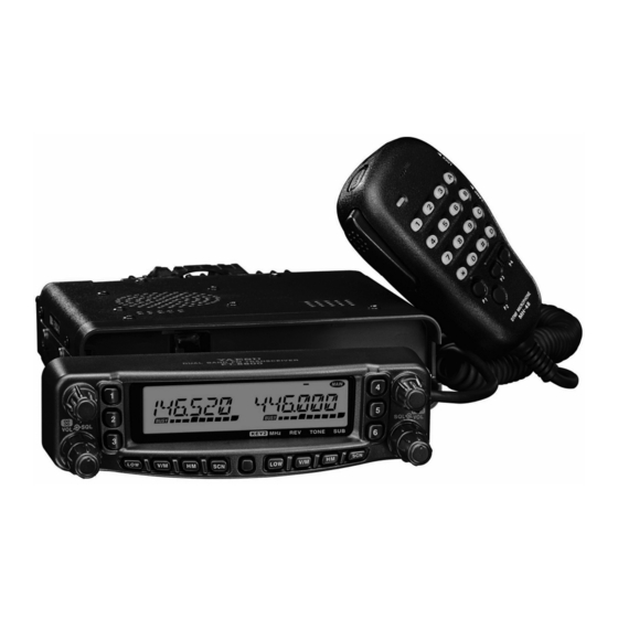
Yaesu FT-8800R Technical Supplement
Dual band fm transceiver
Hide thumbs
Also See for FT-8800R:
- Operating manual (83 pages) ,
- Quick start manual (10 pages) ,
- Basic operations (4 pages)
Advertisement
Dual Band FM Transceiver
FT-8800R
Technical Supplement
©
2003 VERTEX STANDARD CO., LTD.
VOL
This manual provides technical information necessary for servicing the FT-8800R Transceiver.
Servicing this equipment requires expertise in handling surface-mount chip components. Attempts by non-qualified
persons to service this equipment may result in permanent damage not covered by the warranty, and may be illegal in
some countries.
Two PCB layout diagrams are provided for each double-sided circuit board in the transceiver. Each side of thr board is
referred to by the type of the majority of components installed on that side ("leaded" or "chip-only"). In most cases one
side has only chip components, and the other has either a mixture of both chip and leaded components (trimmers, coils,
electrolytic capacitors, ICs, etc.), or leaded components only.
While we believe the technical information in this manual to be correct, Vertex Standard assumes no liability for dam-
age that may occur as a result of typographical or other errors that may be present. Your cooperation in pointing out any
inconsistencies in the technical information would be appreciated.
Specifications ..................................................... 2
Exploded View & Miscellaneous Parts ......... 3
Block Diagram .................................................... 5
Circuit Description ............................................ 7
Alignment ......................................................... 11
( EH018M90A )
1
2
SQL
3
LOW
V/M
HM
SCN
VERTEX STANDARD CO., LTD.
4-8-8 Nakameguro, Meguro-Ku, Tokyo 153-8644, Japan
VERTEX STANDARD
US Headquarters
10900 Walker Street, Cypress, CA 90630, U.S.A.
International Division
8350 N.W. 52nd Terrace, Suite 201, Miami, FL 33166, U.S.A.
YAESU EUROPE B.V.
P.O. Box 75525, 1118 ZN Schiphol, The Netherlands
YAESU UK LTD.
Unit 12, Sun Valley Business Park, Winnall Close
Winchester, Hampshire, SO23 0LB, U.K.
VERTEX STANDARD HK LTD.
Unit 5, 20/F., Seaview Centre, 139-141 Hoi Bun Road,
Kwun Tong, Kowloon, Hong Kong
4
5
6
KEY2
SCN
HM
V/M
LOW
Board Unit (Schematics, Layouts & Parts)
Main Unit ...................................................................... 17
Panel Unit ..................................................................... 45
Panel-Sub Unit ............................................................. 51
VR-L Unit ...................................................................... 53
VR-R Unit ...................................................................... 54
PWR
SQL
VOL
1
Advertisement
Table of Contents

Related Manuals for Yaesu FT-8800R


Summary of Contents for Yaesu FT-8800R
-
Page 1: Table Of Contents
Kwun Tong, Kowloon, Hong Kong KEY2 This manual provides technical information necessary for servicing the FT-8800R Transceiver. Servicing this equipment requires expertise in handling surface-mount chip components. Attempts by non-qualified persons to service this equipment may result in permanent damage not covered by the warranty, and may be illegal in some countries. -
Page 2: Specifications
Specifications ENERAL Frequency Range: 108.000 - 520.000 MHz, 700.000 - 999.995 MHz (Cellular Blocked) 144.000 - 146.000 MHz (or 144.000 - 148.000 MHz), 430.000 - 440.000 MHz (or 430.00 - 450.000 MHz) Channel Steps: 5/10/12.5/15/20/25/50 kHz Modes of Emission: F3, F2 Antenna Impedance: 50-Ohms, unbalanced (Antenna Duplexer built-in) Frequency Stability:... -
Page 3: Exploded View & Miscellaneous Parts
Exploded View & Miscellaneous Parts CS1770001 CASE (W/O NYLON NET) RA02132A0 HIMERON TAPE M4090149 SPEAKER T9206228 RA0415200 (x2 pcs) WIRE ASSY GROUND PLATE T9206438A WIRE ASSY R0150630 HOLDER S5000206 FAN GUARD MAIN UNIT RA0441300 RA0446200 LEAF SPRING RA0438700 M2090034A RUBBER RA02668AA CHASSIS R0137550... - Page 4 Exploded View & Miscellaneous Parts Note:...
-
Page 5: Block Diagram
Block Diagram... - Page 6 Block Diagram Note:...
-
Page 7: Circuit Description
Circuit Description Receiver Signal Path The demodulated “Main” band audio is passed through the de-emphasis network, audio switch D1047 (DAN222), “Main” Band 430 MHz Signal low-pass filter network (consisting of Q1052 (NJM2902V) The 430 MHz signal is passed through a high-pass filter and associated circuitry), and a high-pass filter network network and a low-pass filter network to the antenna (consisting of Q1054 (NJM2904V) and associated circuit-... -
Page 8: Transmitter Signal Path
Circuit Description Meanwhile, a portion of the output of 11.7 MHz crystal Transmitter Signal Path X1003 is multiplied fourfold by Q1043 (2SC4400) to pro- AF Signal vide the 46.8 MHz second local signal, then applied to the The speech signal from the microphone is passed through IF IC Q1047. -
Page 9: Pll Circuit
Circuit Description The 50-Watt RF signal is passed through a low-pass filter 144 MHz network to the antenna switch D1113 and D1114 When the PTT switch is pressed, pin 8 of sub CPU Q2001 (UM9957F), then passed through a high-pass filter net- (M38223M4M) goes “high,”... - Page 10 Circuit Description Power Supply Line “Sub” band A portion of the output from the UHF-VCO/A Q1123 When the user presses and holds in the “Right” VOL knob (2SC5006) is passed through buffer amplifier Q1124 for 2 seconds, pin 23 of the main CPU Q1104 goes “low” (2SC5006) and diode switch D1093 (HVC131) to the pro- and pin 40 of main CPU Q1104 goes “high,”...
-
Page 11: Alignment
Alignment Introduction and Precautions Required Test Equipment The FT-8800R has been carefully aligned at the factory The following test equipment (and thorough familiarity for the specified performance across the 144 MHz and 430 with its correct use) is necessary for complete realignment. - Page 12 Alignment Entering the Alignment mode RF Front-end Tuning Alignment of the FT-8800R is performed using a front-panel 1. Connect the DC voltmeter to TP1020 on the MAIN software-based procedure. To perform alignment of the trans- Unit, then inject a 439.050 MHz signal at a level of +10 ceiver, it must first be placed in the “Alignment Mode,”...
- Page 13 Alignment TX Power Output TX Deviation 1. Press the “Sub” band DIAL knob momentarily, if 1. Press the “Sub” band DIAL knob momentarily, if needed, to switch the “Main” band to be the “Right” needed, to switch the “Main” band to be the “Right” band.
- Page 14 Alignment 10. Press the “Left” band [ LOW ] key. CTCSS Tx Deviation 11. Increase the RF Signal Generator output level to +23 1. Press the “Sub” band DIAL knob momentarily, if dBµ. needed, to switch the “Main” band to be the “Right” 12.
- Page 15 Alignment 49. Press the “Left” band [ V/M ] key. DC Voltmeter 50. Tune the “Left” band frequency to 850.05 MHz. 1. Set the power supply voltage to 13.8 VDC. 51. Inject an 850.05 MHz signal at a level of +3 dBµ from 2.
- Page 16 Note:...
-
Page 17: Main Unit
MAIN Unit Circuit Diagram 45.05 MHz 45.05 MHz (+25.3 dBu) (+15.3 dBu) [+24.3 dBu] [+14.8 dBu] [+13.4 dBu] [+3.0 dBu] [-1.4 dBu] 1.05 V 1.5 V [+17.2 dBu] 0.83 V AM 3.33 V 1.35 V 0.29 V 0.37 V 0.12 V AM 1.95 V 8.56 V 4.97 V... - Page 18 MAIN Unit Note:...
- Page 19 MAIN Unit Parts Layout M3826AEFGP M51132FP BU4066BCFV (Q1104) (Q1063) (Q1071) NJM2902V (Q1052, 1074) BU2090FS TDA7233D (Q1095) (Q1069) MB15A02PFV1 (Q1109, 1112) LA4425A TA31136FN (Q1068) (Q1044, 1047) 2SK2596BX (BX) 2SK2975 DTA144EE (16) (Q1132) (Q1134) (Q1094, 1097, 1101, 1103) 2SA1774 (FR) 2SB1301 (ZQ) 2SC4400 (RT4) (Q1108, 1111) (Q1078)
- Page 20 MAIN Unit M62353GP NJM2902V NJM2904V (Q1105) (Q1053) (Q1054, 1129) TC4W66FU (Q1066, 1067) 2SB1201S AT24C256N (Q1079) (Q1088) NJM78L05 (8C) (Q1084) CPH6102 (AB) S-80823CNMC MM1216 (1C) (Q1064) (Q1085) (Q1080) 2SA1774 (FR) DTC144EE (26) 2SC4400 (RT4) (Q1083) (Q1046, 1049, 1061, (Q1042) 1062, 1065, 1073, 1075, 2SC4617 (BR) 1077, 1089, 1106, 1107, (Q1029, 1031, 1032,...
-
Page 21: Parts List
MAIN Unit Parts List DESCRIPTION VALUE TOL. MFR'S DESIG VXSTD P/N VERS. LOT SIDE LAY ADR PCB with Component CS1795003 TYP: A2U CS1795004 TYP: A1 CS1795005 TYP: A2 CS1795006 TYP: A3 CS1795007 TYP: B1 CS1795008 TYP: B2 CS1795009 TYP: B3 CS1795010 TYP: C1 CS1795011... - Page 22 MAIN Unit DESCRIPTION VALUE TOL. MFR'S DESIG VXSTD P/N VERS. LOT SIDE LAY ADR C 1068 CHIP CAP. 0.001uF GRM36B102K50PT K22178809 C 1070 CHIP CAP. 30pF GRM36CH300J50PT K22178223 C 1071 CHIP CAP. GRM36CH070B50PT K22178294 C 1073 CHIP CAP. 27pF GRM36CH270J50PT K22178222 C 1074 CHIP CAP.
- Page 23 MAIN Unit DESCRIPTION VALUE TOL. MFR'S DESIG VXSTD P/N VERS. LOT SIDE LAY ADR C 1152 CHIP CAP. GRM36CH070B50PT K22178294 C 1153 CHIP CAP. GRM36CK020B50PT K22178289 C 1154 CHIP CAP. GRM36CH060B50PT K22178293 C 1155 CHIP CAP. 22pF GRM36CH220J50PT K22178220 C 1157 CHIP CAP.
- Page 24 MAIN Unit DESCRIPTION VALUE TOL. MFR'S DESIG VXSTD P/N VERS. LOT SIDE LAY ADR C 1238 CHIP CAP. 0.001uF GRM36B102K50PT K22178809 C 1239 CHIP CAP. 0.01uF GRM36B103K16PT K22128804 C 1240 CHIP CAP. 27pF GRM36CH270J50PT K22178222 C 1241 CHIP CAP. 47pF GRM36CH470J50PT K22178228 C 1242...
- Page 25 MAIN Unit DESCRIPTION VALUE TOL. MFR'S DESIG VXSTD P/N VERS. LOT SIDE LAY ADR C 1318 CHIP CAP. 0.022uF GRM36B223K16PT K22128806 C 1319 CHIP CAP. 0.022uF GRM36B223K16PT K22128806 C 1320 CHIP CAP. 0.01uF GRM36B103K16PT K22128804 C 1321 CHIP CAP. 0.0047uF GRM36B472K25PT K22148830 C 1322...
- Page 26 MAIN Unit DESCRIPTION VALUE TOL. MFR'S DESIG VXSTD P/N VERS. LOT SIDE LAY ADR C 1403 CHIP CAP. 0.022uF GRM39B223K25PT K22144807 C 1404 AL.ELECTRO.CAP. 2200uF RE3-16V222M 2200UF K40129064 C 1405 CHIP CAP. 0.47uF GRM40B474K25PT K22140824 C 1406 CHIP CAP. 100pF GRM36CH101J50PT K22178236 C 1407...
- Page 27 MAIN Unit DESCRIPTION VALUE TOL. MFR'S DESIG VXSTD P/N VERS. LOT SIDE LAY ADR C 1484 CHIP CAP. 0.001uF GRM39B102K50PT K22174821 C 1485 CHIP CAP. GRP1553U1H6R0DZ01E K22178307 C 1486 CHIP CAP. 47pF GRP1553U1H470JZ01E K22178319 C 1487 CHIP CAP. 0.001uF GRM36B102K50PT K22178809 C 1489 CHIP CAP.
- Page 28 MAIN Unit DESCRIPTION VALUE TOL. MFR'S DESIG VXSTD P/N VERS. LOT SIDE LAY ADR C 1565 CHIP CAP. 0.01uF GRM36B103K16PT K22128804 C 1566 CHIP CAP. 0.47uF GRM40B474K25PT K22140824 C 1567 CHIP CAP. 0.022uF GRM39B223K25PT K22144807 C 1568 CHIP CAP. 0.001uF GRM36B102K50PT K22178809 C 1569...
- Page 29 MAIN Unit DESCRIPTION VALUE TOL. MFR'S DESIG VXSTD P/N VERS. LOT SIDE LAY ADR C 1647 CHIP CAP. 18pF 200V GRM40CH180J200PT K22230219 C 1648 CHIP CAP. 220pF 200V GRM40CH221J200PT K22230232 C 1649 CHIP CAP. 220pF 200V GRM40CH221J200PT K22230232 C 1650 CHIP CAP.
- Page 30 MAIN Unit DESCRIPTION VALUE TOL. MFR'S DESIG VXSTD P/N VERS. LOT SIDE LAY ADR D 1044 DIODE HSC277TRF G2070584 D 1045 DIODE HSC277TRF G2070584 D 1046 DIODE HSC277TRF G2070584 D 1047 DIODE DAN222 TL G2070174 D 1048 DIODE DAN222 TL G2070174 D 1049 DIODE...
- Page 31 MAIN Unit DESCRIPTION VALUE TOL. MFR'S DESIG VXSTD P/N VERS. LOT SIDE LAY ADR D 1121 DIODE MA2S72800L G2070858 D 1122 DIODE MA2S72800L G2070858 D 1123 SURGE ABSORBER RCCA-201Q43UA Q9000755 D 1125 DIODE MA2S111-(TX) G2070614 FB1001 BEADS COIL B-01-A L1190386 FB1002 FERRITE BEADS SMB304729...
- Page 32 MAIN Unit DESCRIPTION VALUE TOL. MFR'S DESIG VXSTD P/N VERS. LOT SIDE LAY ADR L 1062 M.RFC LK1608 1R0K-T L1690687 L 1063 M.RFC 0.39uH C1608CA-R39G L1691107 L 1064 M.RFC ELJ-ND1R0JF L1690977 L 1065 M.RFC 0.39uH C1608CA-R39G L1691107 L 1066 M.RFC LK1608 1R0K-T L1690687 L 1067...
- Page 33 MAIN Unit DESCRIPTION VALUE TOL. MFR'S DESIG VXSTD P/N VERS. LOT SIDE LAY ADR Q 1025 TRANSISTOR 2SC5006-T1 G3350068 Q 1026 TRANSISTOR 2SC5006-T1 G3350068 Q 1027 TRANSISTOR 2SC4400-3-TL G3344008C Q 1029 TRANSISTOR 2SC4617 TL R G3346178R Q 1030 TRANSISTOR 2SC4617 TL R G3346178R Q 1031 TRANSISTOR...
- Page 34 MAIN Unit DESCRIPTION VALUE TOL. MFR'S DESIG VXSTD P/N VERS. LOT SIDE LAY ADR Q 1108 TRANSISTOR 2SA1774 TL R G3117748R Q 1109 MB15A02PFV1-G-BND-EF G1092541 Q 1110 TRANSISTOR DTC144EE TL G3070075 Q 1111 TRANSISTOR 2SA1774 TL R G3117748R Q 1112 MB15A02PFV1-G-BND-EF G1092541 Q 1113...
- Page 35 MAIN Unit DESCRIPTION VALUE TOL. MFR'S DESIG VXSTD P/N VERS. LOT SIDE LAY ADR R 1057 CHIP RES. 1/16W 0.5% RR0510R-823-D J24189165 R 1059 CHIP RES. 1/16W RMC1/16S 103JTH J24189037 R 1060 CHIP RES. 1/16W RMC1/16S 470JTH J24189009 R 1061 CHIP RES.
- Page 36 MAIN Unit DESCRIPTION VALUE TOL. MFR'S DESIG VXSTD P/N VERS. LOT SIDE LAY ADR R 1138 CHIP RES. 8.2k 1/16W 0.5% RR0510P-822-D J24189141 R 1139 CHIP RES. 1/16W RMC1/16S 331JTH J24189019 R 1140 CHIP RES. 1/16W RMC1/16S 221JTH J24189017 R 1141 CHIP RES.
- Page 37 MAIN Unit DESCRIPTION VALUE TOL. MFR'S DESIG VXSTD P/N VERS. LOT SIDE LAY ADR R 1217 CHIP RES. 100k 1/16W RMC1/16S 104JTH J24189049 R 1218 CHIP RES. 150k 1/16W RMC1/16S 154JTH J24189051 R 1219 CHIP RES. 1/16W RMC1/16S 470JTH J24189009 R 1220 CHIP RES.
- Page 38 MAIN Unit DESCRIPTION VALUE TOL. MFR'S DESIG VXSTD P/N VERS. LOT SIDE LAY ADR R 1294 CHIP RES. 1/16W RMC1/16S 473JTH J24189045 R 1295 CHIP RES. 390k 1/16W RMC1/16S 394JTH J24189056 R 1296 CHIP RES. 390k 1/16W RMC1/16S 394JTH J24189056 R 1297 CHIP RES.
- Page 39 MAIN Unit DESCRIPTION VALUE TOL. MFR'S DESIG VXSTD P/N VERS. LOT SIDE LAY ADR R 1371 CHIP RES. 4.7k 1/16W RMC1/16S 472JTH J24189033 R 1372 CHIP RES. 1/16W RMC1/16S 221JTH J24189017 R 1373 CHIP RES. 1/16W RMC1/16S 221JTH J24189017 R 1374 CHIP RES.
- Page 40 MAIN Unit DESCRIPTION VALUE TOL. MFR'S DESIG VXSTD P/N VERS. LOT SIDE LAY ADR R 1436 CHIP RES. 1/16W RMC1/16S JPTH J24189070 VERSION B1 1- R 1436 CHIP RES. 1/16W RMC1/16S JPTH J24189070 VERSION C1 1- R 1436 CHIP RES. 1/16W RMC1/16S JPTH J24189070...
- Page 41 MAIN Unit DESCRIPTION VALUE TOL. MFR'S DESIG VXSTD P/N VERS. LOT SIDE LAY ADR R 1511 CHIP RES. 470k 1/16W RMC1/16S 474JTH J24189057 R 1512 CHIP RES. 120k 1/16W RMC1/16S 124JTH J24189050 R 1513 CHIP RES. 1/16W RMC1/16S 823JTH J24189048 R 1514 CHIP RES.
- Page 42 MAIN Unit DESCRIPTION VALUE TOL. MFR'S DESIG VXSTD P/N VERS. LOT SIDE LAY ADR R 1588 CHIP RES. 1/16W RMC1/16S 333JTH J24189043 R 1589 CHIP RES. 100k 1/16W RMC1/16S 104JTH J24189049 R 1590 CHIP RES. 2.2k 1/16W RMC1/16S 222JTH J24189029 R 1591 CHIP RES.
- Page 43 MAIN Unit DESCRIPTION VALUE TOL. MFR'S DESIG VXSTD P/N VERS. LOT SIDE LAY ADR R 1668 CHIP RES. 1/16W RMC1/16S 470JTH J24189009 R 1672 CHIP RES. 1/16W RMC1/16S JPTH J24189070 R 1673 CHIP RES. 1/16W RMC1/16S 102JTH J24189025 R 1677 CHIP RES.
- Page 44 MAIN Unit Note:...
-
Page 45: Panel Unit
PANEL Unit Circuit Diagram... - Page 46 PANEL Unit Parts Layout Side A Side B M38223M4M LC75821E TC4W53FU CPH6102 2SA1602A (MF) 2SC4617 (BR) RT1N441U (N3) NJM78L05 (8C) HZM27WA (N3) (Q2001) (Q2002, 2003) (Q2004) (Q2008) (Q2005) (Q2007) (Q2006) (Q2009) (D2004, 2005)
- Page 47 PANEL Unit Parts List DESCRIPTION VALUE TOL. MFR'S DESIG VXSTD P/N VERS. LOT SIDE LAY ADR PCB with Components CB2513001 Printed Circuit Board AH008M000 FR0084500 C 2001 CHIP CAP. 0.001uF GRM36B102K50PT K22178809 C 2002 CHIP CAP. 0.022uF GRM36B223K16PT K22128806 C 2003 CHIP CAP.
- Page 48 PANEL Unit DESCRIPTION VALUE TOL. MFR'S DESIG VXSTD P/N VERS. LOT SIDE LAY ADR R 2014 CHIP RES. 220k 1/16W RMC1/16S 224JTH J24189053 R 2015 CHIP RES. 1/16W RMC1/16S 683JTH J24189047 R 2016 CHIP RES. 1/16W RMC1/16S 473JTH J24189045 R 2017 CHIP RES.
- Page 49 PANEL Unit DESCRIPTION VALUE TOL. MFR'S DESIG VXSTD P/N VERS. LOT SIDE LAY ADR S 2005 TACT SWITCH SKQMAL N5090105 S 2006 TACT SWITCH SKQMAL N5090105 S 2007 TACT SWITCH SKQMAL N5090105 S 2008 TACT SWITCH SKQMAL N5090105 S 2009 TACT SWITCH SKQMAL N5090105...
- Page 50 PANEL Unit Note:...
-
Page 51: Panel-Sub Unit
PANEL-SUB Unit Circuit Diagram... - Page 52 PANEL-SUB Unit Parts Layout NJM2904V (Q 3001) Side A Side B Parts List DESCRIPTION VALUE TOL. MFR'S DESIG VXSTD P/N VERS. LOT SIDE LAY ADR PCB with Components CB2514002 DST: USA CB2514003 DST: EXP CB2514004 DST: AUS Printed Circuit Board AH008M000 FR0085700 C 3001...
-
Page 53: Vr-L Unit
VR-L Unit Circuit Diagram Parts Layout Side A Side B Parts List DESCRIPTION VALUE TOL. MFR'S DESIG VXSTD P/N VERS. LOT SIDE LAY ADR PCB with Components CB2515001 Printed Circuit Board AH018M000 FR0085800 C 4001 CHIP CAP. 0.01uF GRM36B103K16PT K22128804 C 4002 CHIP CAP. -
Page 54: Vr-R Unit
VR-R Unit Circuit Diagram Parts Layout Side A Side B Parts List DESCRIPTION VALUE TOL. MFR'S DESIG VXSTD P/N VERS. LOT SIDE LAY ADR PCB with Components CB2516001 Printed Circuit Board AH008M000 FR0085900 C 5001 CHIP CAP. 0.01uF GRM36B103K16PT K22128804 C 5002 CHIP CAP. - Page 55 Copyright 2003 VERTEX STANDARD CO., LTD. All rights reserved. No portion of this manual may be reproduced without the permission of VERTEX STANDARD CO., LTD.
Need help?
Do you have a question about the FT-8800R and is the answer not in the manual?
Questions and answers