Table of Contents
Advertisement
Quick Links
SERVICE MANUAL
■ CONTENTS
...........................................................3
........................................4
............................................5
..........................................7
...............................................25
...................................................37
.......................................................38
.............................................................44
Test Program .......................................................................................64
........................................................................................71
Inspections ...........................................................................................78
.............................................................................................................83
Updating The Firmware .....................................................................88
....................................................................90
IC & DIODE FIGURES
PA
011947
Copyright (c) NEXO S.A. All rights reserved. PDF ´09.10
Advertisement
Table of Contents

Related Manuals for Nexo NXAMP 4X4


Summary of Contents for Nexo NXAMP 4X4
- Page 1 ...........37 IC BLOCK DIAGRAM ............38 CIRCUIT BOARDS .............44 TEST PROGRAM ..................64 ..................71 INSPECTIONS ...................78 ......................83 UPDATING THE FIRMWARE ..............88 ..............90 PARTS LIST BLOCK DIAGRAM IC & DIODE FIGURES CIRCUIT DIAGRAM 011947 Copyright (c) NEXO S.A. All rights reserved. PDF ´09.10...
- Page 2 NXAMP4x4 WARNING: This product contains chemicals known to the State of California to cause cancer, or birth defects or other reproductive harm. DO NOT PLACE SOLDER, ELECTRICAL/ELECTRONIC OR PLASTIC COMPONENTS IN YOUR MOUTH FOR ANY REASON WHAT SO EVER! Avoid prolonged, unprotected contact between solder and your skin! When soldering, do not inhale solder fumes or expose eyes to solder/flux vapor! If you come in contact with solder or components located inside the enclosure of this product, wash your hands before handling food.
-
Page 3: Panel Layout
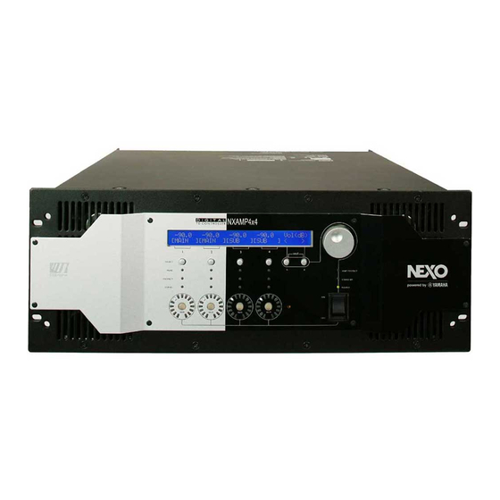
NXAMP4x4 ■ PANEL LAYOUT • Front Panel Power switch Mute buttons Amplifier indicators Select buttons LCD display Channel indicators Encoder Air intakes Navigation buttons (A & B) Screw holes for handles Volume indicators • Rear Panel Mains connectors Balanced audio inputs with link Expansion slot Power outputs RS-232 Firmware update port... -
Page 4: Circuit Board Layout
NXAMP4x4 ■ CIRCUIT BOARD LAYOUT RS232-GPI NX-DFLT PSANHA INANH OPT-AN PAANH PAANH (PA unit) (PA unit) CONTROL Rear Panel NX-DFLT OPT-AN RS232-GPI INANH OUTANH PSANHB PSANHA Front Panel PAANH PAANH (PA unit) (PA unit) PN-AN... -
Page 5: Service Precautions
NXAMP4x4 ■ SERVICE PRECAUTIONS Safety measures • Some component parts on the PSANH circuit board maintain a high voltage even when the power is switched off. For this reason to avoid an electrical shock, do not touch the upper metallic part of the following capacitors until the remaining voltage has discharged. - Page 6 NXAMP4x4 PSANH circuit diagram 220 ohms/10W PSANHA only C205 C201 PSANHB only PSANHA only PSANHA only Primary Secondary 220 ohms/10W 220 ohms/10W C305 C316 C322 C344 C354 C316 D305 C345 C355 C307 To FAN 220 ohms/10W C317 C323 PSANHB PSANHA 220 ohms/10W 5 220 ohms/10W C347...
-
Page 7: Overall Assembly Wiring
NXAMP4x4 ■ OVERALL ASSEMBLY WIRING This product has various cables (wires and connector assemblies) inside. To prevent touching component to the cables and/or connection mistake, perform the cable connection and fixing cables according to the following instructions referring the wiring diagram, P3 of the circuit diagram. - Page 8 NXAMP4x4 2. Wiring of the power switch Install the power switch to the front panel with its terminals set downward. (Fig. 4, 5) Fig. 4 Fig. 5 Confirm that the power switch is set to the off position as shown in the figure. (Fig. 6) Twist the wires of the power switch assembly more than three times.
- Page 9 NXAMP4x4 3. Wiring of the FAN Connect the wire of the FAN to each connector. (Fig. 8) Fig. 8 4. Attaching of the support cushion Attach the support cushion (WN15950) at the specified area on the pattern side of the CONTROL circuit board. (Fig.
- Page 10 NXAMP4x4 5. Wiring of the AC-INLET Set a cord holder before installing the PSANHB circuit board to the enclosure. (Fig. 10) Set a ferrite-core at the specified area on the PSANHB circuit board, and fasten the ferrite-core with a cord holder.
- Page 11 NXAMP4x4 d, e) Fix the wires to the terminal with the screws, and refer to the fig. 14 and fig. 15 for the direction of each terminal. Screw the GND wire’s screw terminal of the upper AC- INLET as shown in the figure, and don’t fasten it with a cord holder.
- Page 12 NXAMP4x4 6. Wiring of the PA unit Connect the wire to the CN401. (Fig. 18, 19, 20 and 21) CN401 Fig. 18 NOTE: The wire to be connected is WK02080. Install this PA unit on the upper left side of enclosure.
- Page 13 NXAMP4x4 CN401 YELLOW Fig. 20 NOTE: The wire to be connected is WK17100. Install this PA unit on the lower left side of enclosure. Hereafter, this unit is called PA unit of CH3. CN401 GREEN Fig. 21 NOTE: The wire to be connected is WK17110. Install this PA unit on the lower right side of enclosure.
- Page 14 NXAMP4x4 Wiring and fastening Connect the following wires at first. CN313: WK68740 CN203: WK66350 Fasten these wires (WK17900, WK17910 and WK94690) with a cord holder to the hexagonal spacer. (Fig. 23) Note: Do not fasten the wires (brown and yellow) of WK94690 because they must be connected to the PSANHA (upper PSANHA) circuit board later.
- Page 15 NXAMP4x4 b-3) Then fasten these wires with a cord holder as shown in the figure. b-4) Fasten these wires (WM04880 x 2, WK16820 x 2) with a cord holder. b-5) Fasten these wires (WN52520 x 2, WK16820 x 2) with a cord holder (2 places). b-6) Fasten these wires (WN52520, WK16820) with a cord holder (1 place).
- Page 16 NXAMP4x4 Connect the wire (WK14210) of the PA unit (CH3) to the connector (CN312) of the PSANHB circuit board. (Draw the black tube to the PA unit side.) Fasten the wire (WK14210) and the wire of the FAN with a cord holder. (Fig. 22) Twist the wires (white, red, black) of the PA unit more than two times, and connect them to the terminals according to the wire color displayed on the PSAN circuit...
- Page 17 NXAMP4x4 At the stage as shown in Fig. 26, connect the following wires. CN313: WK68760 CN201: WK68770 CN202: WK14200 from OUTANH board CN203: WK66350 from PSANHB board h-2) After connecting the wire (WM15830) to it, install the RS232-GPI circuit board to the enclosure. Twist the wires (yellow, brown) of the power switch assembly more than three times, and connect it to the connector (CN103) of the PSANHA circuit board.
- Page 18 NXAMP4x4 Connect the wire (WK14210) of PA unit (CH1) to the connector (CN312) of the PSANHA circuit board. (Draw a black tube to the PA unit side.) Connect the wire (WK14210) of PA unit (CH2) to the connector (CN315) of the PSANHA circuit board. (Draw a black tube to the PA unit side.) Fasten the wire (WK14210) and the wire of FAN with a cord holder as shown in the figure.
- Page 19 NXAMP4x4 Fasten the wires (WK02080, WK17100) with a cord holder to the hole of the RS232-GPI circuit board. (Fig. 28) Fasten the wires (WK02080, WK17100 and WK02070) with a cord holder to the hole of the enclosure. (Fig. 28 *1, 29) Fasten the wires (WK17090, WK17110) with a cord holder to the hole of the enclosure.
- Page 20 NXAMP4x4 Fasten the wires (WK17090 and WK17110) with a cord holder at the hole of the OPT-AN board. Then connect the flat cable (WK02120). (Fig. 30) Fasten the wires (WK02080, WK17090, WK17100, WK17110 and WK02070) with a cord holder at the close area to the OPT-AN circuit board.
- Page 21 NXAMP4x4 8. Color of the connectors connected to the connector CN012–CN015 Connect the connector assembly from the PA unit to the CONTROL circuit board as shown in the figure below. (Fig. 33) CN012 CN013 CN014 CN015 BLUE YELLOW GREEN Fig. 33 9.
- Page 22 NXAMP4x4 10. Insulation distance between wire (WK17110) and primary side capacitor Perform wiring of the connector assembly (WK17110) with care so that its uncovered portion with the SUMI tube does not touch the capacitor (C316) on primary side of the PSANHA circuit board. (Fig. 36, 37) Fig.
- Page 23 NXAMP4x4 12. Confirmation of Switch LED lighting With the front panel 2 uninstalled, confirm that the LEDs of switches (SW003–SW006) light. (Fig. 39) Procedure Press the power switch of this unit to turn on the power. Press the switches (SW003–SW006) on the PN-AN circuit board, and confirm that both LEDs of each switch light.
- Page 24 NXAMP4x4 13. Method of Fixing PN FFC Assembly Fix the PN FFC assembly with the adhesive tape [635] as shown in the figure (2 places). (Fig. 40) 43 mm Match the edge of FFC as shown in the figure. Adhesive tape [635] Fig.
-
Page 25: Disassembly Procedures
NXAMP4x4 ■ DISASSEMBLY PROCEDURES Top Cover and NX-DFLT Card (Time required: about 3 minutes) 1-1. Remove the thirteen (13) screws marked [800]. The top cover can then be removed. (Fig.1) 1-2. Remove the two (2) screws marked [770]. The NX- DFLT card can then be removed. - Page 26 NXAMP4x4 CONTROL Circuit Board, OPT angle and OPT- AN Circuit Board (Time required: about 10 minutes) 2-1. Remove the top cover and the NX-DFLT card. (See procedure 1.) 2-2. Disconnect the connector assemblies from the CONTROL circuit board. (Fig. 2) 2-3.
- Page 27 NXAMP4x4 PSANHA Circuit Board (Time required: about 15 minutes) 3-1. Remove the top cover and the NX-DFLT card. (See procedure 1.) 3-2. Remove the CONTROL circuit board and the OPT angle. (See procedure 2.) 3-3. Remove the two (2) screws marked [150A], and remove the upper ACPS connector assembly.
- Page 28 NXAMP4x4 OUTANH Circuit Board (Time required: about 20 minutes) 4-1. Remove the top cover and the NX-DFLT card. (See procedure 1.) 4-2. Remove the CONTROL circuit board and the OPT angle. (See procedure 2.) 4-3. Remove the PSANHA circuit board. (See procedure 3.) 4-4.
- Page 29 NXAMP4x4 PSANHB Circuit Board (Time required: about 25 minutes) 5-1. Remove the top cover and the NX-DFLT card. (See procedure 1.) 5-2. Remove the CONTROL circuit Board and the OPT angle. (See procedure 2.) 5-3. Remove the PSANHA circuit Board. (See procedure 3.) 5-4.
- Page 30 NXAMP4x4 INANH Circuit Board (Time required: about 7minutes) 6-1. Remove the top cover and the NX-DFLT card. (See procedure 1.) 6-2. Disconnect the connector assembly from the INANH circuit board. (Fig. 6) 6-3. Remove the sixteen (16) screws marked [70]. The INANH circuit board can then be removed.
- Page 31 NXAMP4x4 Upper left (CH1) PA unit (Time required: about 15 minutes) 8-1. Remove the top cover and the NX-DFLT card. (See procedure 1.) 8-2. Remove the CONTROL circuit board and the OPT angle. (See procedure 2.) 8-3. Disconnect the connector assemblies which connects the upper left PA unit and other units.
- Page 32 NXAMP4x4 Lower left (CH3) PA unit (Time required: about 25 minutes) 10-1. Remove the top cover and the NX-DFLT card. (See procedure 1.) 10-2. Remove the CONTROL circuit board and the OPT angle. (See procedure 2.) 10-3. Remove the PSANHA circuit board. (See procedure 3.) 10-4.
- Page 33 NXAMP4x4 Front Panel Assembly (Time required: about 20 minutes) 12-1. Remove the top cover and the NX-DFLT card. (See procedure 1.) 12-2. Remove the CONTROL circuit Board and the OPT angle. (See procedure 2.) 12-3. Disconnect the power switch connector assembly from the PSANHA circuit board.
- Page 34 NXAMP4x4 Upper left DC Fan (Time required: about 15 minutes) 14-1. Remove the top cover and the NX-DFLT card. (See procedure 1.) 14-2. Remove the CONTROL circuit board and the OPT angle. (See procedure 2.) 14-3. Remove the front panel assembly. (See procedure 12.) 14-4.
- Page 35 NXAMP4x4 Lower left DC Fan (Time required: about 23 minutes) 16-1. Remove the top cover and the NX-DFLT card. (See procedure 1.) 16-2. Remove the CONTROL circuit board and the OPT angle. (See procedure 2.) 16-3. Remove the PSANHA circuit board. (See procedure 3.) 16-4.
- Page 36 NXAMP4x4 Power switch (Time required: about 25 minutes) 18-1. Remove the top cover and the NX-DFLT card. (See procedure 1.) 18-2. Remove the CONTROL circuit Board and the OPT angle. (See procedure 2.) 18-3. Disconnect the power switch connector assembly from to the PSANHA circuit board.
-
Page 37: Lsi Pin Description
NXAMP4x4 ■ LSI PIN DESCRIPTION • PCM1803ADBR (X7357B0) A/D CONVERTER CONTROL: IC035, IC036, IC037, IC038 NAME FUNCTION Analog input, L-channel Analog input, R-channel – Reference voltage 1 decoupling capacitor – Reference voltage 2 decoupling capacitor – Analog power supply, 5 V AGND –... -
Page 38: Ic Block Diagram
NXAMP4x4 ■ IC BLOCK DIAGRAM 74HCT273PW,118 (X8681A0) 74LVC169PW,118 (X8482A0) D-type Flip Flop Binaly Counter PN-AN: IC002, 003 CONTROL: IC044, 045 74HCT4514PW,118 (X8630A0) CS3318-CQZ (X8486A0) Decoder Volume Controller PN-AN: IC004-007 CONTROL: IC001 REFI1 RESET OUT5 V CC latch MUTE REFO4 SCL/CCLK SDA/MOSI REFI4 AD0/CS... - Page 39 NXAMP4x4 CS4272-CZZR (X8487A0) DSPB56371AF180 (X8489A0) CODEC CONTROL: IC012, 013 CONTROL: IC022, 023 2.5V to 5V 3.3V to 5V Memory Expansion Area Hardware or Left and Internal Voltage Internal External I2C/SPI Right Mute Triple ESAI ESAI_1 GPIO EFCOP Reference Oscilator Mute Control Control Data Controls Registor/Hardware...
- Page 40 NXAMP4x4 MX25L1605AM2C-12G (X8718A0) (X8718B0) (X6770A0) Flash Memory SHUNT Regulator CONTROL: IC039 PAANH: IC401 PSANH: IC204 CATHOD HOLD# REFERENCE SCLK Address Generator Memory Array Page Buffer ANODE Data Register REFERENCE (R) Y-Decoder ANODE CATHODE SRAM Buffer Output Sense Buffer Amplifire Mode State Logic Machine...
- Page 41 NXAMP4x4 NJU7630-M (X8682A0) PCM1803ADBR (X7357B0) Regulator A/D Converter PSANH: IC205 CONTROL: IC035-038 MODE1 MODE0 FMT1 FMT0 ER.AMP 0.8V AGND SCKI 0.2V PDWN Vref BYPAS DGND TEST DOUT Soft Start LRCK UVLO Latch Delta-Sigma Modulator LRCK Buffer DOUT Serial x 1/64, x 1/128 Interface Decimation 0.5V...
- Page 42 NXAMP4x4 SN74ABT245BNSR (XU009A0) SN74LV14APWR (X6688A0) BUS Transceiver Inverter CONTROL: IC062 CONTROL: IC063 SN74LV273APWR (X5074A0) (X5966A0) D-type Flip Flop Buffer/Driver CONTROL: IC057-061 CONTROL: IC055, 056 PN-AN: IC001 SN74LV4052APWR (X6976A0) SN74LVC00APWR (X5406A0) Demultiplexer NAND CONTROL: IC049 CONTROL: IC040 1-COM 2-COM 1-COM 2-COM...
- Page 43 NXAMP4x4 SN74LVC157APWR (X6786A0) SN74LVC245APWR (XZ287A0) TC74LCX04FT (X8415A0) Data Selector Bas Transceiver Inverter CONTROL: IC046, 051 CONTROL: IC054 CONTROL: IC064 SN74LVC2G74DCTR (X8709A0) Flip Flop CONTROL: IC042 PRE 7 CLK 1 CLR 6 (X8576A0) Regulator PSANH: IC201 DRAIN (7D) CONTROL (1C) INTERNAL SUPPLY SHUNT REGULATOR/ ERROR AMPLIFIER...
-
Page 44: Circuit Boards
NXAMP4x4 ■ CIRCUIT BOARDS CONTENTS • CONTROL Circuit Board (X8710D0) ......46 • INANH Circuit Board (X8714C0) ......45 • LCD SPACER Circuit Board (X8711E0) ......62 • NX-DFLT Circuit Board (YC233A0) ......63 • OPT-AN Circuit Board (X8711E0) ......62 • OUTANH Circuit Board (X8714C0) ......50 •... - Page 45 NXAMP4x4 • INANH Circuit Board to CONTROL CN006 BALANCED INPUTS Component side Pattern side 2NA-WJ97320-10...
- Page 46 NXAMP4x4 • CONTROL Circuit Board to PSANHB to PSANHA to PSANHA to OUTANH CN313 CN313 CN201 CN809, CN810 to PN-AN CN001 Component side 2NA-WR77020-10...
- Page 47 NXAMP4x4 • CONTROL Circuit Board to PAANH to PAANH to PAANH to PAANH to OUTANH (CH1) (CH2) (CH3) (CH4) CN809, CN810 CN401 CN401 CN401 CN401 to INANH W701 to OPT-AN CN301 to RS232-GPI CN201 Component side 2NA-WR77020-10...
- Page 48 NXAMP4x4 • CONTROL Circuit Board Pattern side 2NA-WR77020-10...
- Page 49 NXAMP4x4 • CONTROL Circuit Board Pattern side 2NA-WR77020-10...
- Page 50 NXAMP4x4 • OUTANH Circuit Board to PAANH (CH4) to PAANH (CH3) to PAANH (CH2) to PAANH (CH1) to PSANH W405 ( W405 ( W405 ( W405 ( CN202 ORANGE ORANGE ORANGE ORANGE Speakon D Speakon C Speakon B Speakon A POWER OUTPUTS Component side 2NA-WJ97320-10...
- Page 51 NXAMP4x4 • OUTANH Circuit Board Pattern side 2NA-WJ97320-10...
- Page 52 NXAMP4x4 • PN-AN Circuit Board SELECT PEAK PROTECT SIGNAL MUTE MUTE MUTE Component side 2NA-WJ97170-10...
- Page 53 NXAMP4x4 • PN-AN Circuit Board Encoder AMP PROTECT STAND-BY POWER to CONTROL CN009 MUTE Component side 2NA-WJ97170-10...
- Page 54 NXAMP4x4 • PN-AN Circuit Board Pattern side 2NA-WJ97170-10...
- Page 55 NXAMP4x4 • PN-AN Circuit Board Pattern side 2NA-WJ97170-10...
- Page 56 NXAMP4x4 • PAANH Circuit Board to CONTROL to OUTANH CN012, CN013, CN014, CN015 CN805, CN806, CN807, CN808 to PSANH CN312, CN315 Component side Pattern side 2NA-WR77710-20...
- Page 57 NXAMP4x4 • PAANH Circuit Board to PSANH CN307, CN310 to PSANH CN316, CN309 to PSANH CN305, CN308 Component side Pattern side 2NA-WR77710-20...
- Page 58 NXAMP4x4 • PSANHA, PSANHB Circuit Board Reduction: 7/10 to PAANH W403 to OUTANH W802, W803 to PAANH W404 to PAANH W402 to PAANH W401 to FUN to CONTROL CN007, CN008 to OUTANH W801 to CONTROL CN011 to PSANHB CN203 to FUN to PAANH W401 to PAANH W402 to PAANH W404...
- Page 59 NXAMP4x4 Reduction: 7/10 • PSANHA, PSANHB Circuit Board Component side 2NA-WJ97350-70...
- Page 60 NXAMP4x4 • PSANHA, PSANHB Circuit Board Reduction: 7/10 Pattern side 2NA-WJ97350-70...
- Page 61 NXAMP4x4 Reduction: 7/10 • PSANHA, PSANHB Circuit Board Pattern side 2NA-WJ97350-70...
- Page 62 NXAMP4x4 • RS232-GPI Circuit Board to CONTROL CN010 RS232 GPIO Component side Pattern side • OPT-AN Circuit Board to CONTROL CN017 Expansion slot Component side Pattern side • LCD SPACER Circuit Board Component side Pattern side 2NA-WJ97320-10...
- Page 63 NXAMP4x4 • NX-DFLT Circuit Board Expansion slot Component side Pattern side 2NA-WT66120-10...
-
Page 64: Test Program
NXAMP4x4 ■ TEST PROGRAM Required items Computer : DOS/V computer x1 (Pentium 200MHz or more, Windows XP, USB Port) Software : Software for version up (JTAG Programmer) Cable : RLINK-ST (USB-JTAG adapter) Measuring equipment : Power consumption meter Tools : RS-232C jig x1, GPI jig x1, SLOT jig x1 RS-232C jig SLOT jig /ETH_CS... - Page 65 NXAMP4x4 3. Operation Press the switch displayed on the LCD as instructed one 3-1. Entry of the test program by one. While holding down the [SELECT4], [MUTE4] and [A] If all instructed switches are OK, the display automati- buttons simultaneously, turn the power switch on. The cally returns to the test menu screen.
- Page 66 NXAMP4x4 Lighting order 4-4. LCD test Press the [B] button to continue the test. The test is ex- ecuted automatically. After executing the test, the following display appears. (When an error occurs, “ERROR” appears and the test Press the [B] button to start the test. program is stopped.) First the following display appears.
- Page 67 NXAMP4x4 Switch the GPI jig to the GPO [5:7] position. Press the [B] Press the [B] button to start the test. The following dis- button to continue the test. play appears. The test executes automatically. If the test result is OK, the display automatically returns to the test menu screen.
- Page 68 NXAMP4x4 4-11. FLASH test 4-13. SLOT test Press the [B] button to start the test. The following dis- Rear panel play appears. Expansion slot Press the [B] button to continue the test. The test ex- ecutes automatically. If the test result is OK, the display automatically returns to the test menu screen.
- Page 69 NXAMP4x4 4-15. ANALOG test Input the 1 kHz, +10 dBu sine wave to the channel 2 in- put terminal, and press the [B] button. The analog input level is automatically calibrated, and the following dis- play appears. Press the [B] button to enter the analog test mode. The following display appears.
- Page 70 NXAMP4x4 Input the 1 kHz, +10 dBu sine wave to the channel 4 in- Connect the 8 Ω resistor to the channel 2 output termi- put terminal. nal. Adjust the ENCODER so that the output voltage ob- Adjust the input signal voltage so that the output voltage tained at the channel 4 output terminal is +38.1 dBu, obtained at the channel 2 output terminal is 40 Vrms (= and press the [B] button.
- Page 71 NXAMP4x4 ■...
- Page 72 NXAMP4x4 SWITCH FLASH ENCODER SLOT ATTENUATION RS232 ANALOG BRIDGE PORT (no use) CALIBRATION STANDBY WORD CLOCK QUIT...
- Page 73 NXAMP4x4...
- Page 74 NXAMP4x4...
- Page 75 NXAMP4x4...
- Page 76 NXAMP4x4...
- Page 77 NXAMP4x4...
-
Page 78: Inspections
NXAMP4x4 ■ INSPECTIONS Measurement Conditions 1-1. Environment • Normal temperature: From 10 ˚C to 35 ˚C • Normal humidity: From 45 % to 85 % 1-2. Power Source • When measuring the electrical characteristics, set the power supply voltage and frequency as specified in the table below. - Page 79 NXAMP4x4 1-5. Other 0 dBu is defined as 0.775 Vrms in these inspections. Inspection with ordinary mode Condition: • Ground each input terminal via a 600 Ω resistance. • Do not connect the load resistance to the output terminal. 2-1. Power ON sequence 1) Turn the power switch on.
- Page 80 NXAMP4x4 4-1. Link out Input the 1 kHz, -10 dBu sine wave to each input terminal and confirm that the output voltage obtained at each link out terminal is -10 ±0.5 dBu. 4-2. Efficiency Input the 1 kHz sine wave to the channel 1 input terminal and confirm that the primary power consumption is 500 ±30 W when the output voltage obtained at the channel 1 output terminal is +34.7 dBu.
- Page 81 NXAMP4x4 4-7. Channel separation 1) Ground the channel 2, channel 3 and channel 4 input terminals via a 600 Ω resistor. Input the 1 kHz, 0 dBu sine wave to the channel 1 input terminal and measure the output voltage obtained at the channel 1 output terminal as the reference voltage (0 dB).
- Page 82 NXAMP4x4 Inspection with BRIDGE mode Condition: • Perform each test item in this section with the bridge test mode of the test program. (See “TEST PROGRAM 4-16. BRIDGE test”) • Connect individually the 16 Ω load resistor to channel 1 and channel 3 output terminals. •...
- Page 83 NXAMP4x4 ■ LINK LINK LINK LINK...
- Page 84 NXAMP4x4...
- Page 85 NXAMP4x4...
- Page 86 NXAMP4x4...
- Page 87 NXAMP4x4...
-
Page 88: Updating The Firmware
NXAMP4x4 ■ UPDATING THE FIRMWARE Preparation 1-1. Downloading and installing the software for update 1) Download http://www.st.com/stonline/products/support/micro/files/standalone_jtag.zip. 2) Unpack the StandaloneJTAG_1_20.zip. 3) Double click the StandaloneJTAG_1_20, and the following install screen appears. (Fig. 1) 4) Click the [Finish] button to start installing the software for update. - Page 89 NXAMP4x4 5) Click the [Create] button, and the following JTAG Programmer screen appears. (Fig. 3) 6) Click the [Browse] button and select the desired object file. Check the [All] at Select region, and select Program/Verify at Select operation. Note: This operation is needed when you start up for the first time. Click the [Save] button of save or retrieve JTAG-ISP setup to save the set up file so that this operation will not be required again.
- Page 90 NXAMP4x4 ■...
- Page 91 NXAMP4x4...
-
Page 92: Parts List
NXAMP4x4 PARTS LIST ■ CONTENTS OVERALL ASSEMBLY 1/2 ..........2 2/2 ..........4 PA UNIT ................... 7 LCD ASSEMBLY ................. 9 LOCATIONS OF HEAT SINK UNITS ............10 HEAT SINK UNIT L100 ........11 HEAT SINK UNIT L100 ........12 HEAT SINK UNIT L60 ........ - Page 93 NXAMP4x4 ■ OVERALL ASSEMBLY 1/2 CAUTION The figure below shows the screw marked [555] head shape. To avoid the unit malfunction, make sure the screw marked [555] head shape is same as shown below before assembling the OPT angle. Bottom section (See page 4) LCD Assembly (See page 9)
- Page 94 NXAMP4x4 PART NO. DESCRIPTION REMARKS REF NO. QTY RANK OVERALL ASSEMBLY NXAMP4x4 OVERALL ASSEMBLY (WK66580) OVERALL ASSEMBLY (WK66590) CONNECTOR ASSEMBLY SWPS 2-VH3P AWG22 SW POWER (WK94690) 110a WK75450 0 SWITCH POWER SEESAW JW-M21RKK-NOD U.C. POWER SWITCH WK67150 0 OPT ANGLE AN-PA W J 9 7 15 0 0 CIRCUIT BOARD OPT-AN...
- Page 95 NXAMP4x4 ■ OVERALL ASSEMBLY 2/2 PA Unit (See page 7) PA Unit (See page 7) 140a PA Unit (See page 7) PA Unit (See page 7)
- Page 96 NXAMP4x4 PART NO. DESCRIPTION REMARKS REF NO. QTY RANK WK66830 0 MAIN CHASSIS WK66840 0 MAIN CHASSIS BIND HEAD TAPPING SCREW-B MFZN2B3 (WE96200) 4 W K 74 2 9 0 0 DC FAN ASSEMBLY AN-PA BIND HEAD SCREW 4x16 MFZN2W3 SP (WE98400) 8 HEXAGONAL NUT M4 #1...
- Page 97 NXAMP4x4 PART NO. DESCRIPTION REMARKS REF NO. QTY RANK CORD HOLDER TYTON T18R L100 W2.5 BLACK (WX11230) 11 ACCESSORIES NXAMP4x4 WK60260 0 POWER CORD AASSEMBLY UL25A WK60270 0 POWER CORD AASSEMBLY CCC16A WR94710 0 POWER CORD AASSEMBLY J 30A WN14360 0 LEG ASSEMBLY ✽...
- Page 98 NXAMP4x4 ■ PA UNIT Q524 Q520 Q512P Q510P D503 Q516 Q508P Q506P Q504P Q502P Q514 D506 Q522 Q513P Q511P D504 Q518 Q509P Q507P Q505P Q503P Q501P FRONT REAR D505 Q521 Q513N Q511N D502 Q517 Q509N Q507N Q505N Q503N Q501N Q523 Q519 Q512N Q510N...
- Page 99 NXAMP4x4 PART NO. DESCRIPTION REMARKS REF NO. QTY RANK WR77910 0 PA UNIT AN-PA-HIGH 8F28 HEAT SINK AN-PA-HIGH (WJ94970) HEXAGPNAL SPACER H=7.5 B=5.5 (WD49000) 6 WR77720 0 CIRCUIT BOARD PAANH BIND HEAD TAPPING SCREW-S MFZN2W3 (WE87790) 6 INSULATION SHEET PA-H TBM51W T=0.15 (WK11920) 2 BIND HEAD SCREW 3x12...
- Page 100 NXAMP4x4 ■ LCD ASSEMBLY PART NO. DESCRIPTION REMARKS REF NO. QTY RANK WK75670 0 LCD ASSEMBLY CIRCUIT BOARD PN-AN (WJ97130) CIRCUIT BOARD (WK62420) 2 LCD MODULE CMS-CC2N0124UBSW-W (WJ43880) NYLON RIVET P3570-W/BW (WK67760) 4 ACETATE TAPE #570F W=19 (WG52600) ACETATE TAPE #570F W=19 (WX41610) ✽...
- Page 101 NXAMP4x4 ■ LOCATIONS OF HEAT SINK UNITS Details on PSANHB Circuit Board Heat Sink Unit WK66910 (See page 11) Heat Sink Unit WK66920 (See page 12) Heat Sink Unit WM44760 (See page 17) Heat Sink Unit WK66930 (See page 13) Heat Sink Unit WK66980 (See page 16) Heat Sink Unit WK66940 (See page 14) Details on PSANHA Circuit Board...
- Page 102 NXAMP4x4 ■ HEAT SINK UNIT L100 PSANHB Circuit Board PSANHA Circuit Board WK66910 WK66910 WK66910 PART NO. DESCRIPTION REMARKS REF NO. QTY RANK HEAT SINK UNIT AN-PA-HIGH 100mm (WK66910) BIND HEAD SCREW 3x10 MFZN2W3 (WE95290) 4 INSULATION SHEET RSI T=0.07 (WB44860) 2 HEAT SINK PS L100 ASSY...
- Page 103 NXAMP4x4 ■ HEAT SINK UNIT L100 PSANHB Circuit Board PSANHA Circuit Board WK66920 WK66920 WK66920 PART NO. DESCRIPTION REMARKS REF NO. QTY RANK HEAT SINK UNIT AN-PA-HIGH 100mm (WK66920) BIND HEAD SCREW 3x10 MFZN2W3 (WE95290) 4 INSULATION SHEET RSI T=0.07 (WB44860) 2 HEAT SINK PS L100 ASSY...
- Page 104 NXAMP4x4 ■ HEAT SINK UNIT L60 PSANHB Circuit Board PSANHA Circuit Board WK66930 WK66930 WK66930 PART NO. DESCRIPTION REMARKS REF NO. QTY RANK HEAT SINK UNIT AN-PA-HIGH 60mm (WK66930) BIND HEAD SCREW 3x10 MFZN2W3 (WE95290) 3 HEAT SINK PS L60 ASSY (WM69020) DIODE FMU-36R 20A 600V...
- Page 105 NXAMP4x4 ■ HEAT SINK UNIT L60 PSANHB Circuit Board PSANHA Circuit Board WK66940 WK66940 WK66940 PART NO. DESCRIPTION REMARKS REF NO. QTY RANK HEAT SINK UNIT AN-PA-HIGH 60mm (WK66940) BIND HEAD SCREW 3x10 MFZN2W3 (WE95290) 3 HEAT SINK PS L60 ASSY (WM69020) DIODE FMU-36R 20A 600V...
- Page 106 NXAMP4x4 ■ HEAT SINK UNIT L50 PSANHA Circuit Board WK66950 WK66950 PART NO. DESCRIPTION REMARKS REF NO. QTY RANK HEAT SINK UNIT AN-PA-HIGH 50mm (WK66950) BIND HEAD SCREW 3x10 MFZN2W3 (WE95290) 3 HEAT SINK PS L50 ASSY (WM69030) SCHOTTKY DIODE 10A 60V SF10SC6 (WF41740) NJM7815FA...
- Page 107 NXAMP4x4 ■ HEAT SINK UNIT L50 PSANHB Circuit Board WK66980 WK66980 PART NO. DESCRIPTION REMARKS REF NO. QTY RANK HEAT SINK UNIT 50mm (WK66980) BIND HEAD SCREW 3x10 MFZN2W3 (WE95290) HEAT SINK PS L50 ASSY (WM69030) SCHOTTKY DIODE 10A 60V SF10SC6 (WF41740) ✽...
- Page 108 NXAMP4x4 ■ HEAT SINK UNIT OSH PSANHB Circuit Board WM44760 WM44760 PART NO. DESCRIPTION REMARKS REF NO. QTY RANK HEAT SINK UNIT NX,TX6 25mm (WM44760) BIND HEAD SCREW 3x10 MFZN2W3 (WE95290) HEAT SINK OSH-1625-SFL (WM45790) TOP246YN IPD REGULATOR (X8576A0) ✽ : New Parts RANK: Japan only...
- Page 109 NXAMP4x4 ■ HEAT SINK UNIT MP-5 PAANH Circuit Board WK74640 WK74640 PART NO. DESCRIPTION REMARKS REF NO. QTY RANK HEAT SINK UNIT 10x20 (WK74640) BIND HEAD TAPPING SCREW-B MFZN2W3 (WE93630) HEAT SINK MP-5 (WK74330) TRANSISTOR 2SA1486-AZ M,L,K S (WJ45940) ✽ : New Parts RANK: Japan only...
- Page 110 NXAMP4x4 ■ HEAT SINK UNIT MP-5 PAANH Circuit Board WK74650 WK74650 PART NO. DESCRIPTION REMARKS REF NO. QTY RANK HEAT SINK UNIT 10x20 (WK74650) BIND HEAD TAPPING SCREW-B MFZN2W3 (WE93630) HEAT SINK MP-5 (WK74330) TRANSISTOR 2SC3840-AZ M,L,K S (WJ45950) ✽ : New Parts RANK: Japan only...
-
Page 111: Electrical Parts
NXAMP4x4 ■ ELECTRICAL PARTS PART NO. DESCRIPTION REMARKS REF NO. QTY RANK ELECTRICAL PARTS W R 7 76 5 0 0 CIRCUIT BOARD CONTROL (X8710D0) W J 9 7 2 6 0 0 CIRCUIT BOARD INAN (WJ97320)(X8714C0) W J 9 7 2 8 01 CIRCUIT BOARD OUTANH (WJ97320)(X8714C0) W T 6 6 12 0 0 CIRCUIT BOARD... - Page 112 NXAMP4x4 CONTROL PART NO. DESCRIPTION REMARKS REF NO. QTY RANK C121 CERAMIC CAPACITOR-SL (CHIP) 560pF 50V J (US06256) -124 CERAMIC CAPACITOR-SL (CHIP) 560pF 50V J (US06256) C131 CERAMIC CAPACITOR-B(CHIP) 0.1uF 50V K (WD96920) -136 CERAMIC CAPACITOR-B(CHIP) 0.1uF 50V K (WD96920) C137 MYLAR CAPACITOR (CHIP) 2200pF 50V J...
- Page 113 NXAMP4x4 CONTROL PART NO. DESCRIPTION REMARKS REF NO. QTY RANK C296 CERAMIC CAPACITOR-B(CHIP) 0.1uF 50V K (WD96920) -306 CERAMIC CAPACITOR-B(CHIP) 0.1uF 50V K (WD96920) C307 ELECTROLYTIC CAP.(CHIP) 100uF 16V (UF03810) C308 ELECTROLYTIC CAP.(CHIP) 100uF 16V (UF03810) C309 CERAMIC CAPACITOR-B(CHIP) 0.1uF 50V K (WD96920) C311 CERAMIC CAPACITOR-B(CHIP)
- Page 114 NXAMP4x4 CONTROL PART NO. DESCRIPTION REMARKS REF NO. QTY RANK IC039 MX25L1605DM2I FLASH MEMORY (X8718B0) IC039 MX25L1605AM2C-12G FLASH MEMORY (X8718A0) IC040 SN74LVC00APWR NAND NAND (X5406A0) IC041 MAX3221CPWR RS-232C LINE DRIVER (X2757A0) IC042 SN74LVC2G74DCTR FL FLIP FLOP (X8709A0) IC043 UPSD3354DV (X9170C0) IC044 74LVC169PW,118 4BI BINARY COUNTER...
- Page 115 NXAMP4x4 CONTROL PART NO. DESCRIPTION REMARKS REF NO. QTY RANK R129 CARBON RESISTOR (CHIP) 100 1/16W J (RD35510) R130 CARBON RESISTOR (CHIP) 1/16W J (RD35422) -132 CARBON RESISTOR (CHIP) 1/16W J (RD35422) R133 CARBON RESISTOR (CHIP) 1/16W J (RD35000) R134 CARBON RESISTOR (CHIP) 1/16W J (RD35000)
- Page 116 NXAMP4x4 CONTROL, INAN and OUTANH PART NO. DESCRIPTION REMARKS REF NO. QTY RANK R307 CARBON RESISTOR (CHIP) 47K 1/16W D (RF45747) R308 CARBON RESISTOR (CHIP) 47K 1/16W D (RF45747) R309 CARBON RESISTOR (CHIP) 1.0K 1/16W J (RD35610) -311 CARBON RESISTOR (CHIP) 1.0K 1/16W J (RD35610) R312...
- Page 117 NXAMP4x4 INAN, OUTANH and NX-DFLT PART NO. DESCRIPTION REMARKS REF NO. QTY RANK CN805 FASTEN TERMINAL 16611BL-2 (WA76770) -808 FASTEN TERMINAL 16611BL-2 (WA76770) CN809 CONNECTOR BASE POST PH 16P TE (VF28340) CN810 CONNECTOR BASE POST PH 4P TE (VB39000) D701 DIODE 1SS355 TE-17 (VT33290)
- Page 118 NXAMP4x4 NX-DFLT, OPT-AN, PN-AN and RS232-GPI PART NO. DESCRIPTION REMARKS REF NO. QTY RANK C001 CERAMIC CAPACITOR-F (CHIP) 0.1uF 50V Z (US06510) -011 CERAMIC CAPACITOR-F (CHIP) 0.1uF 50V Z (US06510) CN001 CONNECTOR PHEC 80P SE (WT66950) K001 SCREW TERMINAL M3 8.3x13 M1698 (BB07136) K002 SCREW TERMINAL...
- Page 119 NXAMP4x4 OPT-AN, PN-AN and RS232-GPI PART NO. DESCRIPTION REMARKS REF NO. QTY RANK LD029 LED WHITE (CHIP) WHITE SMLE12WBC7W CH1-VOL14 (WK27910) LD030 LED BLUE (CHIP) BLUE SMLE12BC7T CH1-VOL15 (WK15110) LD032 LED WHITE (CHIP) WHITE SMLE12WBC7W CH2-VOL1 (WK27910) LD033 LED WHITE (CHIP) WHITE SMLE12WBC7W CH2-VOL2 (WK27910)
- Page 120 NXAMP4x4 OPT-AN, PN-AN, RS232-GPI and PAANH PART NO. DESCRIPTION REMARKS REF NO. QTY RANK -012 RESISTOR ARRAY (CHIP) 150x4 J (WG89190) SW001 TACT SWITCH SKRGAED010 VOL-A (WE95200) SW002 TACT SWITCH SKRGAED010 VOL-B (WE95200) SW003 PUSH SWITCH LS22BB-2UR/UR-T MUTE-CH1 (WK74000) SW004 PUSH SWITCH LS22BB-2UR/UR-T MUTE-CH2...
- Page 121 NXAMP4x4 PAANH PART NO. DESCRIPTION REMARKS REF NO. QTY RANK -408 DIODE (CHIP) HSU83 TRF -E (WD84430) D409 DIODE 1SS355 TE-17 (VT33290) -411 DIODE 1SS355 TE-17 (VT33290) D412 ZENER DIODE UDZS3.9B 3.9V (VU17160) D413 ZENER DIODE UDZS6.8BTE-17 6.8V (VU17220) D414 ZENER DIODE UDZS6.8BTE-17 6.8V (VU17220)
- Page 122 NXAMP4x4 PAANH PART NO. DESCRIPTION REMARKS REF NO. QTY RANK R403 THICK FILM RESISTOR (CHIP) 330 1/10W D (RD55533) R404 CARBON RESISTOR (CHIP) 120K 1/4W J (RD15812) -406 CARBON RESISTOR (CHIP) 120K 1/4W J (RD15812) R407 CARBON RESISTOR (CHIP) 220 1/16W J (RD35522) R408 CARBON RESISTOR (CHIP)
- Page 123 NXAMP4x4 PAANH PART NO. DESCRIPTION REMARKS REF NO. QTY RANK R491 CARBON RESISTOR (CHIP) 1/16W J (RD35422) R492 CARBON RESISTOR (CHIP) 1/16W J (RD35422) R493 V 4 8 3 3 2 01 WIRE WOUND RESISTOR 0.22 5W K R494 V 4 8 3 3 2 01 WIRE WOUND RESISTOR 0.22 5W K R495 CARBON RESISTOR (CHIP)
- Page 124 NXAMP4x4 PAANH, PSANHA and PSANHB PART NO. DESCRIPTION REMARKS REF NO. QTY RANK R563 CARBON RESISTOR (CHIP) 10K 1/4W J (RD15710) R564 CARBON RESISTOR (CHIP) 1.0K 1/16W J (RD35610) R565 CARBON RESISTOR (CHIP) 4.7 1/16W J (RD35347) R566 CARBON RESISTOR (CHIP) 4.7 1/16W J (RD35347) R567...
- Page 125 NXAMP4x4 PSANHA and PSANHB PART NO. DESCRIPTION REMARKS REF NO. QTY RANK C201 POLYESTER CAP. 0.047uF 400V K PSANHA (WB68710) C202 ELECTROLYTIC CAP. 47uF (UR85747) C203 ELECTROLYTIC CAP. 22uF (WF20440) C204 ELECTROLYTIC CAP. 22uF (WF20440) C205 ELECTROLYTIC CAP. 100uF 400V (WK76570) C206 CERAMIC CAPACITOR-B(CHIP)
- Page 126 NXAMP4x4 PSANHA and PSANHB PART NO. DESCRIPTION REMARKS REF NO. QTY RANK -329 POLYPROPYLENE CAPACITOR 1.8uF 250V J (WH34340) C330 MONOLITHIC MYLAR CAPACITOR 0.1uF 50V (VR16830) C331 CERAMIC CAPACITOR-B (CHIP) 0.01uF 50V K (US06410) C332 MONOLITHIC MYLAR CAPACITOR 0.1uF 50V (VR16830) C333 CERAMIC CAPACITOR-B (CHIP)
- Page 127 NXAMP4x4 PSANHA and PSANHB PART NO. DESCRIPTION REMARKS REF NO. QTY RANK D221 DIODE (CHIP) RB160L-40 TE25 PSANHA (VS59760) -224 DIODE (CHIP) RB160L-40 TE25 PSANHA (VS59760) D226 DIODE (CHIP) RB160L-40 TE25 (VS59760) D227 DIODE 1SS244 TP (WA18030) D301 DIODE 1SS244 TP (WA18030) D302 DIODE...
- Page 128 NXAMP4x4 PSANHA and PSANHB PART NO. DESCRIPTION REMARKS REF NO. QTY RANK PH202 PHOTO COUPLER TLP781(D4-GR,F) PSANHA (WP38820) PH301 PHOTO COUPLER TLP781(D4-GR,F) (WP38820) -303 PHOTO COUPLER TLP781(D4-GR,F) (WP38820) Q201 TRANSISTOR 2SC2412K Q,R,S PSANHA (VV55640) Q202 DIGITAL TRANSISTOR KRC102S-RTK/P PSANHA (WC43500) Q203 DIGITAL TRANSISTOR KRC102S-RTK/P...
- Page 129 NXAMP4x4 PSANHA and PSANHB PART NO. DESCRIPTION REMARKS REF NO. QTY RANK R228 CARBON RESISTOR (CHIP) 220K 1/16W J (RD35822) R229 CARBON RESISTOR (CHIP) 220K 1/16W J (RD35822) R230 CARBON RESISTOR (CHIP) 1.5K 1/16W J (RD35615) R231 CARBON RESISTOR (CHIP) 220K 1/16W D (RF45822) R232...
- Page 130 NXAMP4x4 PSANHA and PSANHB PART NO. DESCRIPTION REMARKS REF NO. QTY RANK R349 CARBON RESISTOR (CHIP) 1/16W J (RD35422) -352 CARBON RESISTOR (CHIP) 1/16W J (RD35422) R353 CARBON RESISTOR (CHIP) 1.2K 1/16W J (RD35612) R354 CARBON RESISTOR (CHIP) 1.2K 1/16W J (RD35612) R355 CARBON RESISTOR (CHIP)
-
Page 131: Block Diagram
NXAMP4x4 CIRCUIT DIAGRAM ■ CONTENTS IC & DIODE FIGURES ..................... 2 WIRING DIAGRAM ....................3 BLOCK DIAGRAM 1/5 ..........4 2/5 ..........5 3/5 ..........6 4/5 ..........7 5/5 ..........8 OVERALL CIRCUIT DIAGRAM CONTROL 1/6 .................... 9 2/6 ..................10 3/6 ...................11 4/6 .................. -
Page 132: Ic & Diode Figures
NXAMP4x4 ■ IC & DIODE FIGURES LD1117STR (X8495A0) NJM431U (X6770A0) NJM7815FA (XD853A0) NJM78M09DL1A (XZ940A0) REGULATOR REGULATOR REGULATOR +15V REGULATOR +15V CONTROL: IC024 PAANH: IC401 PSANH: IC202, 203 CONTROL: IC006 PSANH: IC204 1: GND 1: INPUT 1: REF 2: VOUT 1: INPUT 2: GND 2: ANODE 3: VIN... - Page 133 NXAMP4x4 ■ WIRING DIAGRAM Note: PSANHA INANH PAANH CONTROL Upper left OUTANH PAANH Upper right PN-AN PAANH Lower left RS232-GPI OPT-AN PAANH Lower right PSANHB 2NC-WK66580-80 3...
- Page 134 NXAMP4x4 ■ BLOCK DIAGRAM 1/5 AC Supply Power Supply Block See Page. 5 Power Switch +24A_B +24A_A ANALOG AUDIO INPUTs +15A Inter-Block Signals [+28dBu]MAX Analog Input Block -15A INANH -> CONTROL AGND Channel 1 GAIN: -14dB ANALOG AUDIO ANA_IN[1:4] Analog Audio Signals ANALOG AUDIO Signals [+14dBu]MAX AGND...
- Page 135 NXAMP4x4 ■ BLOCK DIAGRAM 2/5 SUB POWER SUPPLY 1 MAIN POWER SUPPLY 1 AC (V) B(V) PSANHA 100~120 165~198 220~240 181~198 NOTE) Voltage of +/-B with no LOAD AC VOLTAGE TRANSFORMER DETECT MAIN TRANSFORMER +5VA PS VOLTAGE +B(B) OVERCURRENT DETECT +15VA DETECTOR SWITCHING...
- Page 136 NXAMP4x4 ■ BLOCK DIAGRAM 3/5 PAANH OUTANH +15V Voltage Sensor +15V Total Gain: +37dB -15V EEEngine Current Sensor POUT1 Anti-Oscillation Voltage Limitter Network ANALOG AUDIO INPUTs -15V [+6.8dBu]MAX ANA_OUTx Power Out [+43.8dBu]Max Negative Feedback POUTx +15V Differential Amplifier Stage Voltage Amplifier Stage Power Amplifier Stage Loop Limitter...
- Page 137 NXAMP4x4 ■ BLOCK DIAGRAM 4/5 +3.3D -15A +15A +3.3D RELAY_OUT[1:4] SENSE_U12_DIGI_OUT SENSE_U1 +1.25D +3.3D Serial Flash ROM /RESET_SENSE A/D 2ch 16Mbit 40MHz MCLK,SCLK,LRCK PCM1803A SENSE_U2 CODEC0_DIGI_OUT CODEC1_DIGI_OUT SENSE_U34_DIGI_OUT SENSE_U3 /DSP1_CS CODEC0_DIGI_IN /RESET_SENSE A/D 2ch /RESET_DSP1 ES_I2S_DATA0 MCLK,SCLK,LRCK PCM1803A SENSE_U4 SPI_I/F ES_I2S_DATA1 See page 6 +3.3D...
- Page 138 NXAMP4x4 ■ BLOCK DIAGRAM 5/5 NXAMP4x4 LEVEL DIAGRAM This level diagram is for the purpose of circuit design only. The actual gain structure will depend on the firmware that is used. Input_Amp Input_VR ADC buffer DAC buffer Output_VR Power_Amp Digital Domain (PCB INANH) (PCB Control) (PCB Control)
- Page 139 NXAMP4x4 ■ CIRCUIT DIAGRAM 1/15 (CONTROL 1/6) Note: See parts list for details of circuit board component parts. 28CC1-2001022127-10 0...
- Page 140 NXAMP4x4 ■ CIRCUIT DIAGRAM 2/15 (CONTROL 2/6) Note: XX : Not installed See parts list for details of circuit board component parts. 28CC1-2001022127-20 1...
- Page 141 NXAMP4x4 ■ CIRCUIT DIAGRAM 3/15 (CONTROL 3/6) Not installed Note: XX : Not installed See parts list for details of circuit board component parts. 28CC1-2001022127-30 1...
- Page 142 NXAMP4x4 ■ CIRCUIT DIAGRAM 4/15 (CONTROL 4/6) Note: XX : Not installed See parts list for details of circuit board component parts. 28CC1-2001022127-40 1...
- Page 143 NXAMP4x4 ■ CIRCUIT DIAGRAM 5/15 (CONTROL 5/6) Installed Not installed Note: XX : Not installed See parts list for details of circuit board component parts. 28CC1-2001022127-50 3...
- Page 144 NXAMP4x4 ■ CIRCUIT DIAGRAM 6/15 (CONTROL 6/6) to PSANHA_CN201 <P.22: A3> to INANH_W701 <P.15: D2> to PAANH_CN401 <P.20: P4> to PSANH_CN313 <P.23: B6> to PSANH_CN313 <P.23: B6> to OUTANH_CN809 <P.16: M1> to OUTANH_CN810 <P.16: L1> to PN-AN_CN001 to RS232-GPI_CN201 to OPT-AN_CN301 <P.17: O2>...
- Page 145 NXAMP4x4 ■ CIRCUIT DIAGRAM 7/15 (INANH) to CONTROL_CN006 <P.14: J2> Note: See parts list for details of circuit board component parts. 28CC1-2001022114-10 2...
- Page 146 NXAMP4x4 ■ CIRCUIT DIAGRAM 8/15 (OUTANH) to PSANH_CN202 to CONTROL_CN016 <P.22: A5> <P.14: B7> CN306 to PAANH_W405 <P.20: F6> CN306 to PSANH_CN306 <P.23: B2> to PSANH_CN317 CN306 <P.23: B7> CN306 Note: See parts list for details of circuit board component parts. 28CC1-2001022114-20 1...
- Page 147 NXAMP4x4 ■ CIRCUIT DIAGRAM 9/15 (PN-AN) to CONTROL_CN009 <P.14: J9> Note: XX : Not installed 28CC1-2001022128-10 3 See parts list for details of circuit board component parts.
- Page 148 NXAMP4x4 ■ CIRCUIT DIAGRAM 10/15 (RS232-GPI) to CONTROL_CN010 <P.14: G9> Note: See parts list for details of circuit board component parts. 28CC1-2001022128-20 1...
- Page 149 NXAMP4x4 ■ CIRCUIT DIAGRAM 11/15 (OPT-AN, NX-DFLT) Not installed Expansion slot Not installed to CONTROL_CN017 <P.14: B9> See parts list for details of circuit board component parts. See parts list for details of circuit board component parts. 28CC1-2001022128-30 0 28CC1-2001057627-10 0...
- Page 150 NXAMP4x4 ■ CIRCUIT DIAGRAM 12/15 (PAANH) to PSANH_CN305 <P.23: B2> to PSANH_CN308 <P.23: B7> to CONTROL_CN012 <P.14: B1> to CONTROL_CN013 <P.14: B3> to CONTROL_CN014 <P.14: B4> to CONTROL_CN015 <P.14: B5> to PSANH_CN309 CN316 <P.23: B7> to PSANH_CN316 <P.23: A2> to OUTANH_CN805 to OUTANH_CN807 <P.16: P3>...
- Page 151 NXAMP4x4 ■ CIRCUIT DIAGRAM 13/15 (PSANHA/PSANHB 1/3) to PSANH_W101 <P.22: L3> Primary Secondary to PSANH_W102 <P.22: L4> Note: See parts list for details of circuit board component parts. 28CC1-2001022145-10 5...
- Page 152 NXAMP4x4 ■ CIRCUIT DIAGRAM 14/15 (PSANHA/PSANHB 2/3) PSANHA only Primary Secondary PSANHB only PSANHA only PSANHA only to OUTANH_W101 <P.21: B2> to CONTROL_CN011 <P.14: G2> to OUTANH_W102 <P.21: B6> PSANHA only PSANHA only PSANHB only to OUTANH_W801 <P.16: O2> PSANHB only PSANHA only PSANHA only PSANHA only PSANHA only...
- Page 153 NXAMP4x4 ■ CIRCUIT DIAGRAM 15/15 (PSANHA/PSANHB 3/3) Primary Secondary to OUTANH_W802 to PAANH_W402 <P.16: F6> <P.20: A2> to OUTANH_W803 <P.16: F7> to PAANH_W403 J, U models <P.20: A6> to PAANH_W404 <P.20: A10> To FAN CHN model to PAANH_W401 <P.20: P10> PSANHB PSANHA to CONTROL_CN007...
Need help?
Do you have a question about the NXAMP 4X4 and is the answer not in the manual?
Questions and answers