
Related Manuals for Philips HTR3154


Summary of Contents for Philips HTR3154
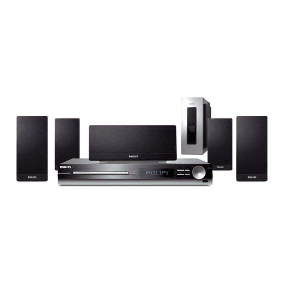
- Page 1 DVD Home Theatre System HTS3154/ 12/05 3139 785 32690(05) 3139 785 32720(12)
-
Page 2: Location Of Pcb Boards
LOCATION OF PCB BOARDS TUNER PCB STANDBY PCB MAIN PCB POWER PCB CONTROL PCB PHONE PCB VOL PCB USB PCB VERSION VARIATION: HTR3154 Type/Version Feature & Board in used Main PCB ( Power Output 300W) Power Voltage ( 230V ) Scart... - Page 3 Sp ecifi c ations AMPLIFIER FRONT AND REAR SPEAKERS Total output power: 300 W RMS System: Full range satellite Frequency Response: 180 Hz – 18 kHz / ±3 dB Impedance: 4 Ω Signal-to-Noise Ratio: >60 dB (A-weighted) Speaker drivers: 3” full range speaker Input Sensitivity Frequency response: 150 Hz –...
- Page 4 Measurement Setup Tuner FM Bandpass Tuner AM (MW,LW) Bandpass...
- Page 5 SERVICE AIDS ESD Equipment: Service Tools: Anti-static table mat - large 1200x650x1.25mm ...4822 466 10953 Universal Torx driver holder .........4822 395 91019 anti-static table mat - small 600x650x1.25mm ..4822 466 10958 Torx bit T10 150mm ...........4822 395 50456 Anti-static wristband ..........4822 395 10223 Torx driver set T6-T20 .........4822 395 50145 Connectorbox (1M ..........4822 395 11307...
- Page 6 WAARSCHUWING WARNING Alle IC’s en vele andere halfgeleiders zijn All ICs and many other semi-conductors are gevoelig voor electrostatische ontladingen susceptible to electrostatic discharges (ESD). (ESD). Careless handling during repair can reduce life Onzorgvuldig behandelen tijdens reparatie kan drastically. de levensduur drastisch doen verminderen. When repairing, make sure that you are Zorg ervoor dat u tijdens reparatie via een connected with the same potential as the mass...
- Page 7 You will find this and more technical information • Use only lead-free solder alloy Philips SAC305 with within the “magazine”, chapter “workshop news”. order code 0622 149 00106. If lead-free solder-paste is required, please contact the manufacturer of your For additional questions please contact your local solder-equipment.
- Page 8 2 - 1 2 - 1 System , Region Code , etc. Setting Produre 1)System Reset 6)Upgrading new sofeware a) press “system “ buttom on R/C,TV show “setup“ a)open the CD Door,then insert the CD-R program disc b) select the menu using the on R/C b)close the DOOR c) go preference page to do sysytem reset...
- Page 9 2 - 2 2 - 2 REPAIR INSTRUSTRATOR...
- Page 10 3 - 1 3 - 1 Dismantling of the Main PCB DISASSEMBLY INSTRUCTIONS 2) Return the set to its upright position and remove the Tray Cover as shown in Figure 3 and close the tray manually by 1) Loosen 4 screw “ A “ on the top of main board as shown in pushing it back in.
- Page 11 3 - 2 3 - 2 Dismantling of the Control Board Dismantling of the DVD Module 1) Loosen 12 screws “ C” at the back pancle as shown in fi gure 6 1) Loosen 4 screws “E” to remove the DVD Module as shown in fi gure 9 Figure 6 Dismantling of the Power Board...
- Page 12 4 - 1 4 - 1 BLOCK DIAGRAM CONTROL PCB MAIN PCB POWER PCB...
- Page 13 4 - 2 4 - 2 WIRING DIAGRAM MAIN PCB USB PCB VOL PCB POWER PCB DVD LOADER VFD PCB CONTROL PCB...
- Page 14 5 - 1 5 - 1 FTD DISPLAY PIN ASSIGNMENT CONTROL BOARD TABLE OF CONTENTS FTD Display Pin Assignment ............. 5-1 Voltage ....................5-2 Circuit Diagram .................. 5-3 PCB Layout Top & Bottom View ............5-4 Electrical Parts List ................5-5...
- Page 15 5 - 2 5 - 2 VOLTAGE Q200 Pin NO Voltage -0.9 Pin NO Voltage -18.9 -25.3 -25.3 -25.3 -25.3 -16.4 23.2 Pin NO Voltage -18.6 -1836 -20.8 -25.3 -25.3 -16.5 -18.7 -16.5 -25.4 -25.4 23.2 -25.7 -23.2 -23.2 -23.2 -23.2 -23.2 -23.2 Pin NO Voltage -23.2 -23.2 -23.2 -23.2...
- Page 16 5 - 3 5 - 3 CIRCUIT DIAGRAM C200 A2 C206 B2 C212 B2 C218 C4 C227 B4 D202 B1 IC200 B1 R202 A2 R208 C1 R214 C2 R226 C3 SN200 B2 TA205 C4 ZD202 C4 C201 A2 C207 B2 C213 C2 C219 C1 C288 A4...
- Page 17 5 - 4 5 - 4 PCB LAYOUT - TOP VIEW C208 D203 JW13 R200 R215 SN200 B3 USB200 A2 C209 DP200 B2 JW14 JW20 R201 R219 TA200 VR200 A3 C216 JW15 JW21 R202 RB200A A4 TA201 XL200 CN203 A3 JW16 JW22 R203...
- Page 18 6 - 1 6 - 1 INTERNAL IC DIAGRAM - CO4558A HOSP MAIN BOARD TABLE OF CONTENTS Internal IC Diagram ................6-1 Circuit Diagram .................. 6-2 PCB Layout Top View ............... 6-3 PCB Layout Bottom View ..............6-4 Voltage ....................6-5 INTERNAL IC DIAGRAM - V5888S HOSP...
- Page 19 6 - 2 6 - 2 Circuit Diagram C1001 D3 C139 C372 C547 CN103 B1 L302 R136 R335 R815 C1002 D3 C140 C373 C548 CN104 B1 L307 R137 R336 R816 C1003 D3 C141 C374 C549 CN301A B1 L308 R138 R337 R817 C1004 D3 C142...
- Page 20 6 - 3 6 - 3 PCB Layout Top View C1020 C153 C326 C391 C537 C812 CN801 FB1104 A1 IC1101 L508 R106 R136 R175 R314 R349 R405 R818 ZD1101 A1 C1023 C155 C327 C392 C538 C813 CN802 FB1107 A1 IC302 L511 R107 R137...
- Page 21 6 - 4 6 - 4 PCB Layout Bottom View C1001 C1013 C1101 C1117 C117 C136 C183 C309 C401 C425 C507 C558 C810 C851 L101 R117 R3016 R510 R814 C1002 C1015 C1102 C1118 C118 C139 C186 C310 C403 C426 C508 C572 C811 C852...
- Page 22 6 - 5 6 - 5 Voltage Pin NO Pin NO Voltage Voltage Pin NO Pin NO Voltage Voltage Pin NO Pin NO Voltage Voltage Pin NO Pin NO Voltage Voltage Pin NO Voltage Pin NO Pin NO Voltage Voltage 30.9 30.9 15.2...
- Page 23 7 - 1 7 - 1 VOLTAGE Pin NO Voltage Pin NO Voltage Pin NO Voltage Pin NO Voltage POWER BOARD Pin NO Voltage Pin NO Voltage Q901 Q902 Q903 Q904 Pin NO Pin NO Pin NO Pin NO Voltage -0.8 -0.8 -0.8...
-
Page 24: Circuit Diagram
7 - 2 7 - 2 CIRCUIT DIAGRAM BD901 C913 C925 C937 C949 C962 C975 D906 D919 IC905 Q902 Q914 R911 R924 R936 R948 R960 R972 R984 ZD907 C901 C914 C926 C938 C950 C963 C976 D907 D922 L901 Q903 Q915 R912 R925 R937... - Page 25 7 - 3 7 - 3 PCB LAYOUT - TOP VIEW BD901 A1 C909 C922 C961 C974 D907 D926 C3 J903 J912 J921 J930 L908 Q911 B2 R930 R948 R980 ZD906 A3 C901 C911 C1 C923 C962 C975 D908 D927 J904 J913 J922...
- Page 26 7 - 4 7 - 4 PCB LAYOUT - BOTTOM VIEW C910 C927 C934 C944 C954 C972 C1 D910 Q904 A2 R905 C3 R915 R922 R935 R947 R958 R969 R977 ZD903 B2 C913 C928 C935 C946 C1 C955 C977 D911 Q905 A1 R906 R916...
- Page 27 8 - 1 DVD BOARD TABLE OF CONTENTS EXPLORER VIEW ................8-2 MECHANICAL PART LIST ..............8-3...
- Page 28 8 - 2 EXPLORER VIEW...
- Page 29 8 - 3 MECHANICAL PART LIST Loc. Part No. Description BPM206009-0202 TRAY FMT020202-XXXX TRAY MOTOR HSP243174-1030 SCREW BPG206006-0001 GEAR-G POM BPG206014-0001 GEAR PULLER POM HSW258064-1040 SCREW BPG206026-0001 GEAR TRAY1 BPG206027-0001 GEAR TRAY - 2 BPG206028-0001 GEAR TRAY - 3 HSW248004-1060 SCREW BRW206004-0001 RUBB BELT...
- Page 30 9 - 1 9 - 1 Mechanical Exploded View...
- Page 31 9 - 2 9 - 2 MECHANICAL PART LIST Loc. Part No. Description 996510001639 DVD DOOR 996510001640 DISPLAY LENS 996510001641 VOL KNOB 996510001642 FRONT CABINET 994000005305 RUBBER FOOT 996510001631 PHONE JACK PCB 996510001643 FUNCTION KEY BASE 996510001644 EJECT BUTTON BASE 996510001645 EJECT BUTTON 996510001646...
Need help?
Do you have a question about the HTR3154 and is the answer not in the manual?
Questions and answers