LG Flatron F700B Service Manual
Color monitor
Hide thumbs
Also See for Flatron F700B:
- Service manual (40 pages) ,
- Service manual (59 pages) ,
- User manual (19 pages)
Table of Contents
Advertisement
Quick Links
COLOR MONITOR
SERVICE MANUAL
CHASSIS NO. : CA-113
FACTORY MODEL: FB770G
MODEL:
*(
) ID LABEL Model No.
CAUTION
BEFORE SERVICING THE UNIT,
READ THE SAFETY PRECAUTIONS IN THIS MANUAL.
Website:http://biz.LGservice.com
E-mail:http://www.LGEservice.com/techsup.html
F700B
(FB770G-EA)
775FT Plus
(FB770G-EA)
Advertisement
Table of Contents

Subscribe to Our Youtube Channel
Related Manuals for LG Flatron F700B


Summary of Contents for LG Flatron F700B
-
Page 1: Color Monitor
Website:http://biz.LGservice.com E-mail:http://www.LGEservice.com/techsup.html COLOR MONITOR SERVICE MANUAL CHASSIS NO. : CA-113 FACTORY MODEL: FB770G MODEL: F700B (FB770G-EA) 775FT Plus (FB770G-EA) ) ID LABEL Model No. CAUTION BEFORE SERVICING THE UNIT, READ THE SAFETY PRECAUTIONS IN THIS MANUAL. -
Page 2: Table Of Contents
CONTENTS SPECIFICATIONS ........... 2 ADJUSTMENT ............11 SAFETY PRECAUTIONS ........3 TROUBLESHOOTING GUIDE ......13 TIMING CHART ............4 EXPLODED VIEW........... 23 OPERATING INSTRUCTIONS ........ 5 REPLACEMENT PARTS LIST ....... 25 WIRING DIAGRAM ..........6 PIN CONFIGURATION........... 30 DISASSEMBLY ............7 SCHEMATIC DIAGRAM ......... -
Page 3: Safety Precautions
SAFETY PRECAUTIONS SAFETY-RELATED COMPONENT WARNING! X-RADIATION There are special components used in this color monitor The only potential source of X-radiation is the picture tube. which are important for safety. These parts are marked However, when the high voltage circuitry is operating on the schematic diagram and the replacement properly there is no possibility of an X-radiation problem. -
Page 4: Timing Chart
TIMING CHART VIDEO SYNC << Dot Clock (MHz), Horizontal Frequency (kHz), Vertical Frequency (Hz), Horizontal etc... (µs), Vertical etc... (ms) >> Sync Total Period Video Active Sync Duration Front Porch Blanking Time Back Porch Resolution Mode Frequency Time (A) Polarity Sort –... -
Page 5: Operating Instructions
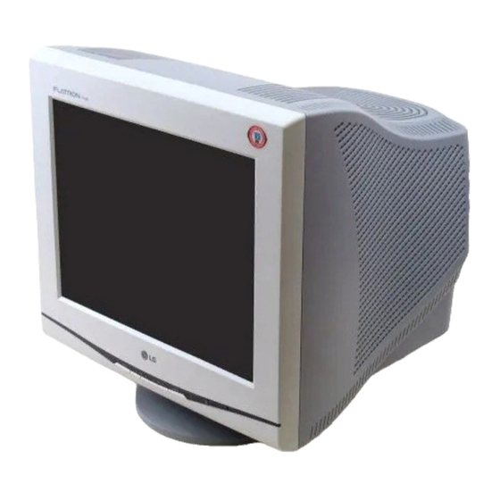
OPERATING INSTRUCTIONS FRONT VIEW REAR VIEW AC Power Socket See Front Control Panel Power Button D-Sub Signal Connector Front Control Panel 1. Power Button Button Use these buttons to choose or adjust items in This button is used to turn the monitor ON and the on screen display. -
Page 6: Wiring Diagram
WIRING DIAGRAM P201 P402 P405 P502 P501 P702 P701 Socket P902 Signal Cable P302 P301 - 6 -... -
Page 7: Disassembly
DISASSEMBLY 1. TILT/SWIVEL & BACK COVER REMOVAL 1) Set the monitor face downward. 2) Carefully remove the Tilt/Swivel by pulling it upward. 3) Pressing the latch (a), Back cover by pushing it upward. (See Figure. 1) 4) Release the latch (b). (See Figure. 2 and Tip Spec.) 5) Slide the Back Cover away from the Front Cabinet of the monitor. -
Page 8: Block Diagram
BLOCK DIAGRAM Dynamic Focus Static Focus Screen(G2) - 8 -... -
Page 9: Description Of Block Diagram
DESCRIPTION OF BLOCK DIAGRAM 1. Line Filter & Associated Circuit. 6. Horizontal and Vertical Oscillation. This is used for suppressing noise of power input line This circuit generates the horizontal pulse and the vertical flowing into the monitor and/or some noise generated in pulse by taking the H and V sync signal. - Page 10 15. Image Rotation (Tilt) Circuit. 17. Video Output Amp Circuit. This circuit corrects the tilt of the screen by supplying the This circuit amplifies the video signal which comes from image rotation signal to the tilt coil which is attached near the video pre-amp circuit and amplified it to applied the the deflection yoke of the CRT.
-
Page 11: Adjustment
ADJUSTMENT GENERAL INFORMATION All adjustment are thoroughly checked and corrected 10) Adjust balance of pin-balance as arrow keys to be when the monitor leaves the factory, but sometimes the best condition. 11) DIST. ADJ. → FOS. ADJ command. several adjustments may be required. Adjustment should be following procedure and after 12) Adjust V-SIZE as arrow keys to 230 ±... - Page 12 4. Input EDID Data. 17-1) Adjust R-DRIVE and G-DRIVE command to white 1) Display color 15,0 cross hatch pattern at Mode 4. ± 0.003 and y=0.298 ± 0.003 on the balance x=0.283 2) EEPROM → Write EDID command and confirm White Balance Meter with PC arrow keys.
-
Page 13: Troubleshooting Guide
TROUBLESHOOTING GUIDE 1. NO POWER NO POWER (POWER INDICATOR OFF) CHECK TROUBLE IN FUSE FUSE OK? (F901) CHECK C908 VOLTAGE? TROUBLE IN (AC120V: 160VDC, D900 AC220V: 304VDC) CHECK IC901 PIN 6 TROUBLE IN WAVEFORM (SQUARE WAVE IC901 COMES OUT?) CHECK TROUBLE IN D941, D942, D951, D961, D941, D942, D951,... - Page 14 2. NO CHARACTER NO CHARACTER CHECK TROUBLE IN IC302 P302 5V LINE PIN 9(5V) ? TROUBLE IN CHECK PC SIGNAL, IC302 PIN 5, 6, 7? P301 SIGNAL CABLE CHECK TROUBLE IN IC302 PIN 20, 19, 18 ? IC302 CHECK TROUBLE IN IC303 PIN 4 (80V) P303 12V LINE/ PIN 8 (12V) ?
- Page 15 3. NO RASTER NO VIDEO (POWER INDICATOR ON) CHECK AMBER DPM MODE POWER INDICATOR (NO H and/or V SYNC) GREEN or AMBER? GREEN CHECK TROUBLE IN D712 ANODE D712 (-157V)? CHECK TROUBLE IN G1 VOLTAGE? Q799 (-55V~-150V) CHECK TROUBLE IN CDT HEAT D941, Q942, Q941 VOLTAGE? (6.3V)
- Page 16 4. NO HORIZONTAL DEFLECTION NO H-DEFLECTION (ONE VERTICAL LINE) CHECK TROUBLE IN Q706? Q706 CHECK TROUBLE IN B + VOLTAGE 50V LINE (50V)? CHECK T701(FBT) PIN 2 TROUBLE IN (31KHZ 60V, Q719, Q720, D710 69KHZ 140V) ? CHECK TROUBLE IN Q701 COLLECTOR Q701 WAVEFORM?
-
Page 17: Trouble In H-Linearity
5. TROUBLE IN H-LINEARITY UNBALANCED OF H-LIN. CHECK TROUBLE IN IC401 IC401 (MICOM) PIN 5, 6, 7 ? CHECK TROUBLE IN Q711~Q716? Q711 ~ Q716 CHECK TROUBLE IN L703? L703 Cs SIGNAL TABLE HORIZONTAL FREQUENCY(fH) TROUBLE IN 30K ~ 34.9K C722, C723, C726, C729 35K ~ 38.9K 39K ~ 44.9K... - Page 18 6. NO VERTICAL DEFLECTION NO V-DEFLECTION (ONE HORIZONTAL LINE) CHECK TROUBLE IN IC601 PIN 3 R603 15V LINE (15V)? TROUBLE IN CHECK HIGH-VOLTAGE OUT IC601 PIN 7 CIRCUIT(FBT), (40V)? D721, R606 CHECK TROUBLE IN IC701 PIN 12, 13? IC701 TROUBLE IN IC601, V-CIRCUIT - 18 -...
- Page 19 7. TROUBLE IN OSD (ENTER BUTTON MUST BE PRESSED.) NO OSD CHECK TROUBLE IN IC301 B + 5V LINE (5V) ? DC 5V CHECK TROUBLE IN IC301 PIN 5, 10 IC601 PIN8 (V-FBP), WAVEFORM? T701 40V LINE (H-FBP) Pin 10 Pin 5 CHECK TROUBLE IN...
- Page 20 8. TROUBLE IN DPM (NO OFF MODE.) OFF MODE FAILURE CHECK CHECK PC, IC401 (MICOM) INPUT H/V SYNC SIGNAL (PC IS NOT GOING INTO PIN 31, 32 (H/V INPUT) DPM OFF MODE) SIGNAL? H/V SYNC CHECK TROUBLE IN IC401 PIN 13 X401 WAVEFORM? 24MHz...
-
Page 21: No Degaussing
9. NO DEGAUSSING NO DEGAUSSING (DEGAUSS ON THE OSD MENU MUST BE PRESSED.) CHECK TROUBLE IN IC401 PIN 19 IC401 (MICOM) (0V)? CHECK TROUBLE IN Q953 COLLECTOR Q953 VOLTAGE? DC 15V CHECK TROUBLE IN P902 ? P902 CHECK TROUBLE IN RL901? RL901 TROUBLE IN... - Page 22 10. NO TILT (NO ROTATION ) NO TILT (NO ROTATION) CHECK TROUBLE IN IC401 PIN21 IC401 ( MI COM) WAVE FORM ? CHECK 15V LINE TROUBLE IN 15V LINE, 6.3V LINE AND 6.3V LINE ? CHECK TROUBLE IN Q503 EMITTER Q501~Q503 VOLTAGE ? TROUBLE IN...
- Page 23 - 23 -...
-
Page 24: Exploded View Parts List
CABINET ASSEMBLY, FB770G BRAND 068 DI F700B 3091TKC074A CABINET ASSEMBLY, FB770G BRAND 068 FOR JAPAN 2423GC3E41M CDT(CIRC), M41QBF423X 31NPLD LG-PHILIPS Displays 70KHZ 29.1 mm For Northern Hemisphere or 2423GC3E41B CDT SET, M41QBF423X 31N6LD For Northern Hemisphere 2423GC3E41U CDT(CIRC), M41QBF423X 32SPLD LG-PHILIPS Displays 70KHZ 29.1 mm For Southern Hemisphere 2423GC3E41N CDT(CIRC), M41QBF423X 31RPLD LG-PHILIPS Displays 70KHZ 29.1 mm For Equatorial... -
Page 25: Replacement Parts List
REPLACEMENT PARTS LIST CAUTION: BEFORE REPLACING ANY OF THESE COMPONENTS, READ CAREFULLY THE SAFETY PRECAUTIONS IN THIS MANUAL. * NOTE SAFETY Mark AL ALTERNATIVE PARTS DATE: 2002. 05. 13. DATE: 2002. 05. 13. *S *AL LOC. NO. PART NO. DESCRIPTION / SPECIFICATION *S *AL LOC. - Page 26 DATE: 2002. 05. 13. DATE: 2002. 05. 13. *S *AL LOC. NO. PART NO. DESCRIPTION / SPECIFICATION *S *AL LOC. NO. PART NO. DESCRIPTION / SPECIFICATION C747 0CK3320W515 3300P 500V K B D311 0DS124409AA 1SS244 TP ROHM KOREA C748 181-288B MKT 100V 104JTR PHS26104 D312 0DS124409AA...
- Page 27 100 1/4W(3 5% TA52 Q701 0TR200009AB KTC200-Y TP KEC TO92 NPN R331 0RD1000Q609 100 1/4W(3 5% TA52 Q706 0TR558900BA 2SC5589(LG,W/M) BK TOSHIBA TO3 R332 0RD1000Q609 100 1/4W(3 5% TA52 Q707 0TR127009AA KTA1270-Y(KTA562TM) TP KEC TO9 R333 0RD1000Q609 100 1/4W(3 5% TA52...
- Page 28 DATE: 2002. 05. 13. DATE: 2002. 05. 13. *S *AL LOC. NO. PART NO. DESCRIPTION / SPECIFICATION *S *AL LOC. NO. PART NO. DESCRIPTION / SPECIFICATION R388 0RD1000Q609 100 1/4W(3 5% TA52 R709 0RD2202Q609 22K 1/4W(3 5% TA52 R389 0RD1000Q609 100 1/4W(3 5% TA52 R710 0RD1000Q609...
- Page 29 0RD2001Q609 2K 1/4W(3 5% TA52 6631T11005D 1P W-T 520MM UL 1015 AWG 22 CB R805 0RD2001Q609 2K 1/4W(3 5% TA52 T701 6174T11003E “1054A,CB777G LG-PHILIPS 17””” R806 0RD4702Q609 47K 1/4W(3 5% TA52 T702 6170TCZ013A EI2218 26UH D/FOCUS,FB775G R808 0RD6802Q609 68K 1/4W(3 5% TA52...
-
Page 30: Pin Configuration
PIN CONFIGURATION TDA4866J Current Driven Vertical Deflection Booster SYMBOL OUTB TDA4866J OUTB OUTA V FB GUARD OUTA FEEDB GUARD FEEDB Pin Configuration M24C08 Serial I C BUS EEPROM SYMBOL DESCRIPTION PSDIP8 (BN) 0.25mm Frame E0-E2 Chip Enable Input Serial Data Address Input/Output Serial Clock Write Control SO8 (MN) -
Page 31: Schematic Diagram
SCHEMATIC DIAGRAM IIC-SDA NOTICE IIC-SCL Since this is a basic schematic diagram. The value of components and some partial connection are DDC-SDA sucject to be changed for improvement without notice. DDC-SCL - 31 - - 32 -... -
Page 32: Printed Circuit Board
PRINTED CIRCUIT BOARD 1. CONTROL BOARD (Component Side) 2. CONTROL BOARD (Solder Side) 3. MAIN BOARD (Component Side) 4. MAIN BOARD (Solder Side) - 33 - - 34 -... - Page 33 May. 2002 P/NO : 3828TSL065P Printed in Korea...
Need help?
Do you have a question about the Flatron F700B and is the answer not in the manual?
Questions and answers