Advertisement
Service
Manual
POWER ON/OFF
SECTION .....................................................................................................................................PAGE
1. TECHNICAL SPECIFICATIONS ................................................................................................... 1
2. SERVICE PROCEDURE............................................................................................................... 2
3. SERVICE MODE........................................................................................................................... 6
4. BLOCK DIAGRAM ........................................................................................................................ 7
5. SCHEMATIC DIAGRAM................................................................................................................ 9
6. PARTS LOCATION...................................................................................................................... 23
7. IC DATA ....................................................................................................................................... 27
8. EXPLODED VIEW AND PARTS LIST ......................................................................................... 33
9. ELECTRICAL PARTS LIST ......................................................................................................... 37
Please use this service manual with referring to the user guide ( D.F.U. ) without fail.
Printed on 100% Recycled Paper
Printed in Japan
CD PLAYER CD7300
OPEN/CLOSE
TIMER
DISC
TTL
DISPLAY
OFF
TEXT 1 2
1
2
3
TABLE OF CONTENTS
CD7300
CD7300 /
DISPLAY
RNDM
PROG
A Ð B
RPT
1
S.PLAY
TRK
INDX
TTL
TIME
EASY JOG
MP3
3 4
5 6
7 8
9 10 11 12 13 14 15 16 17 18 19 20
QUICK REPLAY
4
5
6
7
8
9
0
F1N/K1G/S1G/C1G
/N1G/N1B
CD Player
STOP
PLAY/PAUSE
/
LEVEL
PHONES
-
+
R
Part no. 05AK855020
First Issue 2003.07
ecm
Advertisement
Table of Contents

Related Manuals for Marantz CD7300


Summary of Contents for Marantz CD7300
-
Page 1: Table Of Contents
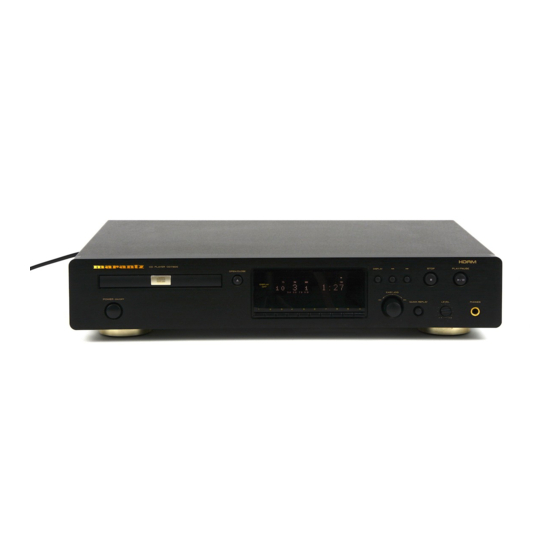
Service CD7300 / F1N/K1G/S1G/C1G /N1G/N1B Manual CD Player CD PLAYER CD7300 DISPLAY STOP PLAY/PAUSE OPEN/CLOSE TIMER RNDM PROG A Ð B S.PLAY DISC INDX TIME DISPLAY EASY JOG TEXT 1 2 9 10 11 12 13 14 15 16 17 18 19 20... - Page 2 Parts for your MARANTZ equipment are generally available to our National Marantz Subsidiary or Agent. ORDERING PARTS : Parts can be ordered either by mail or by Fax.. In both cases, the correct part number has to be specifi ed.
-
Page 3: Technical Specifications
1. TECHNICAL SPECIFICATIONS Audio characteristics Channels .................................2 channels Frequency response ............................2 Hz to 20 kHz Dynamic range ................................100 dB Signal-to-noise ratio...............................110 dB Channel separation ............................100 dB (1 kHz) Harmonic distortion ............................0.0025% (1 kHz) Wow & fl utter .............................. Precision of quartz Error correction system ........................ -
Page 4: Service Procedure
2. SERVICE PROCEDURE Emergency Eject To open the stucked tray, insert a pin into the eject pinhole and push the eject lever. Use a pin φ4mm or less. This picture shows the unit upside down. The eject lever is pointed by the arrow. The lever is thin so aim the narrow area carefully. - Page 5 Cautions in Assembling and Disassembling When removing the flat wire PS01, connecting the optical pick up and the CD decorder board, short-cut the two lands pointed by the arrow with solder. Otherwise the laser diode may be damaged by static electricity. CD Decorder Board (PS01) Repair When Repairing the CD decorder board PS01, you can fix the board on the loader unit as shown in the pictuer below with the flat wires that are provided as service parts.
- Page 6 Disk Tray Open/Close Speed Adjustment Open/Close speed of the tray can be changed. When vibration occurs upon tray open/close and some unusual behavior happens, change the tray speed to stop vibration. Description of the terms displayed on FL start T-On Time open T-PushTm T-Push Tm...
- Page 7 Disc Tray Open/Close Speed Disc Tray open/close speed Tray open/close Tray open/close speed Tray Display start T-On Time open T-PushTm T-Push Tm Tray open Tray open open start 0 2550ms T-OffTim T-On Time High start T-On Time close 0 255ms T-Push Tm T-OffTim Tray close...
-
Page 8: Service Mode
3. SERVICE MODE Turning into Service Mode DISPLAY QUICK REPLAY POWER While pressing DISPLAY and QUICK REPLAY buttons, press POWER button. P 0 0 Mode0 (Display : Ver : P00 Version number of the micro computer is displayed) Status: [FOCUS OFF] [SPINDLE OFF] [RADIAL OFF] [MUTE ON] •... -
Page 9: Block Diagram
4. BLOCK DIAGRAM OPTICAL SCLK/WCLK/ LD/MON CD-ROM & MP3 DECODER DATA SAA7324H/M2B STA016T TZA1024 LDON PULSE ADALAS CD DECODER VAM2202/04 TRANS RF AMP 16.9MHz CDRW COAXIAL COPPER CASE CD10 16.9MHz PHILIPS D2-D4 CD TEXT HDAM LC89170M CS4396 Discrete D1-D5 SANYO CIRRUS INSW SUB CODE... -
Page 10: Schematic Diagram
5. SCHEMATIC DIAGRAM TP823 TP820 Q806 79L24 D808 -28V TP817 Q802 C831 C816 C834 C818 7809 470/50 100/35 R807 R808 TP818 C832 C830 TP819 100R 100R C801 10n(DM) 470/16 1000/35 +9VA R881 R803 D807 D801 11EQS10 C808 TP814 D813 J008 W802 R804 1SS176... - Page 11 R211 R212 R213 TP135 TP137 Q113 Q114 2SC4081 2SC4081 TP136 TP138 J101 FPC15 +5VA Q101 R110 RAD- TZA1024T/N1 R101 FOC+ TRACKING TP103 TP104 1.8V FOC- C106 TP148 TP146 TP144 2.4V 2.3V 47/6.3 RAD+ FOCUS TP149 TP147 TP145 C104 Laser 0.8V 2.3V C107 47/6.3...
- Page 12 Radial Radial FOCUS R195 +3.3V FOCUS +3.3V Sledge Sledge C193 MOTO1 MOTO1 R199 R194 DOBM 220R +5VD C175 C153 C158 INSW INSW Laser Laser C154 R154 C155 VRin VRin C151 R174 SBS Y 1.3V 0.1V TP176 SFSY 1.3V 1.6V R153 1.3V R166 C152...
- Page 13 RM14 +2.7V CM06 QM02 LM01 100n +3.3V 2SC4672 +2.7V BL02RN2R1M2B TPM02 RM08 CM22 CM09 100n RM06 CM21 +2.7V CM02 100n RM19 100/10 CM16 MGND MGND 100n 470R J103 CM23 100/10 TPY31 TPY33 TPY35 TPY37 TPY39 TPY41 TPY43 TPY45 TPY46 TPY48 TPY50 TPY52 SYM No.
- Page 14 C311 220/16V (to FRONT) SR01 INT/EXT_SW C411 220/16V D403 D303 R311 R313 1SS302 1SS302 L:INT R407 R409 120R 120R Q311 Q411 R333 120R 120R H:EXT 2SK170V 2SK170V 10k0 Q307 +9VA Q401 Q407 Q301 Q305 C309 Q405 2SA1312B 2SA1312B 2SK369 2SA1312B 150p 2SK389 R309...
- Page 15 MP_RES CY05 MP_RQST MP_RQST RY05 CY04 100n RY07 +5VD +5VD +5VD XY01 JY03 RR23 DR02 1SS301 QR21 RY14 2SC4081 +5VD DM:Dummy RR21 RY15 CSTCC10.0M (Not use) RR22 RY01 CY14 CY15 +5VD CD7300 QY02 CY06 BD4742G-TR 100n SYM No. PS01 WG05AK1030...
- Page 16 +5VD RF24 220R DF02 CF11 VF01 FL_OFF 13-ST-35G 9 10 11 12 13 14 15 16 17 18 19 20 21 22 23 24 25 26 27 28 29 30 31 32 33 34 35 36 37 38 39 40 41 42 43 44 45 JF01 FFC20P TPF01...
-
Page 17: Parts Location
6. PARTS LOCATION PM01 QN03 Q806 D807 D808 QN06 QN07 DN09 QN08-QN11 DN01-DN04 D806 D801-D804 QN05 QN04 D816 DN05 QN01 QN02 D805 Q808 D815 Q807 Q805 D810 Q801 D813 Q802 D814 Q803 PP01 QD03 D301-D305(Odd) D401-D405(Odd) Q427 Q603 QD02 Q301-Q315(Odd) Q401-Q409(Odd) Q411 Q613... - Page 18 PS01 DR02 QR21 Q104 QM02 QM01 QY03 Q201 QY01 QY02 Q153 Q113 Q101 Q114 Q150 Q152 Q102 Q112 D101 Q110 D102 Q105 Q103 Q106-108 Q111 Q109 Q154...
-
Page 19: Ic Data
7. IC DATA QY02:BD4742G Pin Assignment ( 5 ) ( 4 ) 1pin : N.C. 2pin : SUB 3pin : GND 4pin : Vout 5pin : Vcc ( 1 ) ( 2 ) ( 3 ) Q153:BU2630FV Pin descriptions QD01:CS4396 Pin Description Reset VREF... - Page 20 QM01:STA016 Pin Description Pin Name Type Description Sourde/Dest CDDSP interface CD_LRCK DSP Interface left/right Clock From DSP CD_SDI DSP interface serial data From DSP CD_BCK DSP interface bit clock From DSP SDI interface BS_SDI Bitstream interface serial data From MCU BS_LRCK Bitstream interface left/right Clock From MCU...
-
Page 21: Pin Assignment
Pin Name Type Description Sourde/Dest HANDSHAKE SIGNALS Strobe signal From MCU RQST I2C data signal To MCU C LINK I2C clock signal From MCU I2C data signal To MCU MISCELLANEOUS Oscillator input Oscillator output CLKOUT Buffered output clock -RESET Reset -TESTEN Reserved for test purpose FILT0... - Page 22 Q150:SAA7324 Pin Description SYMBOL DESCRIPTION HFREF comparator common mode input HFIN comparator signal input ISLICE current feedback output from data slicer analog ground 1 SSA1 analog supply voltage 1 DDA1 reference current output pin reference voltage for servo ADC's unipolar current input (central diode signal input) unipolar current input (central diode signal input) unipolar current input (central diode signal input) unipolar current input (central diode signal input)
- Page 23 QY01:µPD784216A Pin No. Port Name I/O Signal Name Pull up Initial Remarks Pin No. Port Name I/O Signal Name Pull up Initial Remarks P120/RTP0 O n.c. n.c. P86/A6 O n.c. n.c. P121/RTP1 O n.c. n.c. P87/A7 O n.c. n.c. P122/RTP2 O n.c.
-
Page 24: Exploded View And Parts List
8. EXPLODED VIEW AND PARTS LIST 5 4 0 5 3 ( M) 5 1 2 9 3 X 8 ( M) 5 1 2 6 SYMB OL ST YLE PAR TS NAME MARK MATERIAL /FINISH 3 X8 ( M) 5110 +B . - Page 25 NOT STANDARD SPARE PARTS 001D BLACK LID TOP COVER BLACK 349K257020 001D GOLD LID TOP COVER GOLD 349K257120 001S PACKING CASE 05AK801010 002S CUSHION 386K809010 NOTE : "nsp" PART IS LISTED FOR REFERENCE ONLY, MARANTZ WILL NOT SUPPLY THESE PARTS.
- Page 26 VERS. PART NO. PART NO. DESCRIPTION COLOR (FOR EUR) (MJI) QP40410986 SUSPENSION(4822 404 10986) QP40410986 QP40111709 CLAMPER(4822 401 11709) QP40111709 QP35810266 BELT(4822 358 10266) QP35810266 NOTE : "nsp" PART IS LISTED FOR REFERENCE ONLY, MARANTZ WILL NOT SUPPLY THESE PARTS.
-
Page 27: Electrical Parts List
12. ELECTRICAL PARTS LIST NOTE ON SAFETY FOR FUSIBLE RESISTOR : ASSIGNMENT OF COMMON PARTS CODES. RESISTORS The suppliers and their type numbers of fusible resistors : 1) GD05 × × × 140, Carbon film fixed resistor, ±5% 1/4W are as follows; : 2) GD05 ×... - Page 28 ELECT. 100µF M 35V RA-2 OA10703520 PH01-RESISTORS C835 CER. CHIP 0.1µF GRM39F104Z16 DK98104200 R901 RM01031170 VARIABLE RK09L12B0 10K RM01031170 C836 CER. CHIP 0.1µF GRM39F104Z16 DK98104200 B(D-CUT REVERSE) NOTE : "nsp" PART IS LISTED FOR REFERENCE ONLY, MARANTZ WILL NOT SUPPLY THESE PARTS.
- Page 29 R329-R332 R425-R428 R801-R804 R406 R407 PM01-SEMICONDUCTORS CHIP 120Ω ±5% 1/16W NN05121610 D301 HZ21005000 CHIP DIODE 1SS301 DAN202U HZ21005000 R410 D302 HZ21005000 CHIP DIODE 1SS301 DAN202U HZ21005000 NOTE : "nsp" PART IS LISTED FOR REFERENCE ONLY, MARANTZ WILL NOT SUPPLY THESE PARTS.
- Page 30 HC3890509F C115 CER. CHIP 1000pF ±10% B 50V DK96102300 Q802 HC3890909F IC REG. NJM7809FA +9V 1A HC3890909F C116 CER. CHIP 1000pF ±10% B 50V DK96102300 NOTE : "nsp" PART IS LISTED FOR REFERENCE ONLY, MARANTZ WILL NOT SUPPLY THESE PARTS.
- Page 31 CM15 CER. CHIP 1µF 10V F DK98105200 R151 CHIP 470Ω ±5% 1/16W NN05471610 CM16 CER. CHIP 0.1µF GRM39F104Z16 DK98104200 R152 CHIP 1MΩ ±5% 1/16W NN05105610 NOTE : "nsp" PART IS LISTED FOR REFERENCE ONLY, MARANTZ WILL NOT SUPPLY THESE PARTS.
- Page 32 FQ01005020 CERAMIC VIB. CSTCC10.0MG FQ01005020 RM54 RESONATOR 10MHz RR21 CHIP 10kΩ ±5% 1/16W NN05103610 RR22 CHIP 2.2kΩ ±5% 1/16W NN05222610 RR23 CHIP 10kΩ ±5% 1/16W NN05103610 NOTE : "nsp" PART IS LISTED FOR REFERENCE ONLY, MARANTZ WILL NOT SUPPLY THESE PARTS.
- Page 33 T001 /F MAINS TRANSF. TS15725190 EI57-25 100V 50/60HZ T001 /K MAINS TRANSF. TS15725200 EI57-25 110V/220V 50/60HZ T001 /C/N/S TS15725210 MAINS TRANSF. TS15725210 EI57-25 230V 50HZ NOTE : "nsp" PART IS LISTED FOR REFERENCE ONLY, MARANTZ WILL NOT SUPPLY THESE PARTS.
Need help?
Do you have a question about the CD7300 and is the answer not in the manual?
Questions and answers