Table of Contents
Advertisement
SERVICE MANUAL
Main Section
I Specifications
I Preparation for Servicing
I Adjustment Procedures
I Schematic Diagrams
I CBA's
I Exploded views
I Parts List
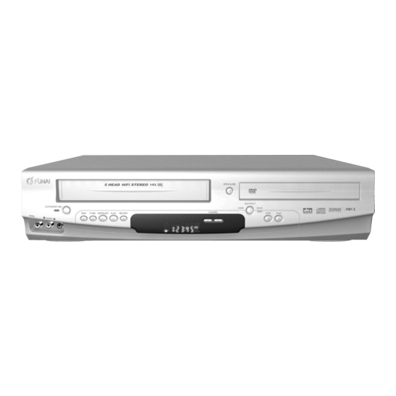
VIDEO CASSETTE RECORDER
DVD PLAYER &
DPVR-6600
DPVR-6630
When servicing the deck
mechanism, refer to MK14 Deck
Mechanism Section.
Deck Mechanism Part No.:
N25E0FL
PAL
Advertisement
Table of Contents

Subscribe to Our Youtube Channel
Related Manuals for FUNAI DPVR-6600

Summary of Contents for FUNAI DPVR-6600
- Page 1 I Specifications mechanism, refer to MK14 Deck I Preparation for Servicing Mechanism Section. I Adjustment Procedures I Schematic Diagrams Deck Mechanism Part No.: I CBA’s I Exploded views N25E0FL I Parts List DVD PLAYER & VIDEO CASSETTE RECORDER DPVR-6600 DPVR-6630...
-
Page 2: Table Of Contents
MAIN SECTION DVD PLAYER & VIDEO CASSETTE RECORDER DPVR-6600/DPVR-6630 Main Section I Specifications I Preparation for Servicing I Adjustment Procedures I Schematic Diagrams I CBA’s I Exploded Views I Parts List TABLE OF CONTENTS Specifications ............... . . 1-1-1 Laser Beam Safety Precautions . -
Page 3: Specifications
SPECIFICATIONS < VCR Section > Description Unit Minimum Nominal Maximum Remark 1. Video 1-1. Video Output (PB) Vp-p SP Mode 1-2. Video Output (R/P) Vp-p SP Mode, 1-3. Video S/N Y (R/P) W/O Burst 1-4. Video Color S/N AM (R/P) SP Mode 1-5. - Page 4 < DVD Section > ITEM CONDITIONS UNIT NOMINAL LIMIT 75 Ω load 1. Video Output ± 0.1 2. Optical Digital Out 3. Audio (PCM) 1 kHz 0 dB, 47k Ω load 3-1. Output Level Vrms 47k Ω load 3-2. S/N 3-3.
-
Page 5: Laser Beam Safety Precautions
LASER BEAM SAFETY PRECAUTIONS This DVD player uses a pickup that emits a laser beam. Do not look directly at the laser beam coming from the pickup or allow it to strike against your skin. The laser beam is emitted from the location shown in the figure. When checking the laser diode, be sure to keep your eyes at least 30 cm away from the pickup lens when the diode is turned on. -
Page 6: Important Safety Precautions
IMPORTANT SAFETY PRECAUTIONS Product Safety Notice K. Crimp type wire connector The power transformer uses crimp type connectors Some electrical and mechanical parts have special which connect the power cord and the primary side safety-related characteristics which are often not evi- of the transformer. - Page 7 Safety Check after Servicing Examine the area surrounding the repaired location for damage or deterioration. Observe that screws, Chassis or Secondary Conductor parts, and wires have been returned to their original positions. Afterwards, do the following tests and con- Primary Circuit Terminals firm the specified values to verify compliance with safety standards.
-
Page 8: Standard Notes For Servicing
STANDARD NOTES FOR SERVICING Circuit Board Indications Pb (Lead) Free Solder When soldering, be sure to use the Pb free solder. 1. The output pin of the 3 pin Regulator ICs is indi- cated as shown. How to Remove / Install Flat Pack-IC Top View Bottom View 1. - Page 9 3. The flat pack-IC on the CBA is affixed with glue, so With Soldering Iron: be careful not to break or damage the foil of each (1) Using desoldering braid, remove the solder from all pin or the solder lands under the IC when removing pins of the flat pack-IC.
- Page 10 2. Installation (4) Bottom of the flat pack-IC is fixed with glue to the CBA; when removing entire flat pack-IC, first apply (1) Using desoldering braid, remove the solder from soldering iron to center of the flat pack-IC and heat the foil of each pin of the flat pack-IC on the CBA up.
- Page 11 Instructions for Handling Semi-conductors Electrostatic breakdown of the semi-conductors may occur due to a potential difference caused by electro- static charge during unpacking or repair work. 1. Ground for Human Body Be sure to wear a grounding band (1MΩ) that is prop- erly grounded to remove any static electricity that may be charged on the body.
-
Page 12: Preparation For Servicing
PREPARATION FOR SERVICING How to Enter the Service Mode About Optical Sensors Caution: An optical sensor system is used for the Tape Start and End Sensors on this equipment. Carefully read and follow the instructions below. Otherwise the unit may operate erratically. What to do for preparation Insert a tape into the Deck Mechanism Assembly and press the PLAY button. -
Page 13: Cabinet Disassembly Instructions
CABINET DISASSEMBLY INSTRUCTIONS 1. Disassembly Flowchart REMOVAL This flowchart indicates the disassembly steps to gain REMOVE/*UNHOOK/ LOC. PART Fig. access to item(s) to be serviced. When reassembling, UNLOCK/RELEASE/ Note follow the steps in reverse order. Bend, route, and UNPLUG/DESOLDER dress the cables as they were originally. 5(S-8), 2(S-9), (S-10), [1] Top Case Chassis Unit... - Page 14 Reference Notes CAUTION 1: Locking Tabs (L-1) and (L-2) are fragile. Be careful not to break them. (S-1) (S-1) 1-1. Release three Locking Tabs (L-1). [1] Top Case 1-2. Release three Locking Tabs (L-2), then remove the Front Assembly. CAUTION 2: Electrostatic breakdown of the laser (S-1) diode in the optical system block may occur as a potential difference caused by electrostatic charge...
- Page 15 CN401 (S-3) CN601 (S-9) (S-8) (S-3) (S-8) [4] DVD Mechanism (S-9) Assembly (S-3) (S-4) [5] Partition Plate (S-8) (S-5) (S-6) CN501 (S-10) [9] VCR Chassis Unit [7] Loader Holder [6] Power Supply CBA (L-3) Fig. D5 Fig. D3 (S-7) (S-7) [8] DVD Main CBA Unit CN301...
- Page 16 Cylinder Assembly FE Head ACE Head Assembly [10] Deck Assembly SW507 Lead with blue stripe LD-SW [13] Jack-A CBA (S-11) (S-13) [12] Main CBA [10] Deck Assembly (S-13) Cam Gear [12] Main CBA Desolder (S-11) Hole Shaft from bottom [11] DVD (S-12) Open/Close CBA Hole...
- Page 17 HOW TO EJECT MANUALLY 1. Remove the Top Case, Front Assembly and Top Bracket. 2. Remove four Screws (S-3) in Fig. D3. Do not disconnect connectors. 3. While lifting up the DVD Mechanism, rotate the roulette in the direction of the arrow as shown below.
-
Page 18: Electrical Adjustment Instructions
ELECTRICAL ADJUSTMENT INSTRUCTIONS General Note: "CBA" is an abbreviation for "Circuit Board Assembly." NOTE: Figure 1 1.Electrical adjustments are required after replacing circuit components and certain mechanical parts. It is important to do these adjustments only after all repairs and replacements have been com- EXT. -
Page 19: How To Initialize The Dvd Player & Vcr
HOW TO INITIALIZE THE DVD PLAYER & VCR To put the program back at the factory-default, initialize the DVD player & VCR as the following procedure. < DVD Section > 1. Press [DVD], [1], [2], [3], [4], and [DISPLAY] buttons on the remote control unit in that order. Fig. -
Page 20: Firmware Renewal Mode
FIRMWARE RENEWAL MODE 1. Turn the power on and remove the disc on the tray. 5. After programming is finished, the tray opens automatically. Fig. e appears on the screen and 2. To put the DVD player into version up mode, press the checksum in (*2) of Fig. - Page 21 10. Press [CLEAR] button on the remote control unit. Fig. h appears on the screen. " ******* " differ depending on the models. MODEL : ******* Version : *.** Region : * EEPROM CLEAR : OK EEPROM CLEAR : CLEAR EXIT: POWER Fig.
-
Page 22: Function Indicator Symbols
FUNCTION INDICATOR SYMBOLS Note: If a mechanical malfunction occurs, the power is turned off. When the power comes on again after that by pressing [FUNCTION] button, an error message is displayed on the TV screen for 5 seconds. MODE INDICATOR ACTIVE When reel or capstan mechanism is not “A R”... -
Page 23: Block Diagrams
BLOCK DIAGRAMS <VCR SECTION> Servo / System Control Block Diagram H9900BLS 1-11-1... - Page 24 Video Block Diagram H9900BLV 1-11-2...
- Page 25 Audio Block Diagram H9900BLA 1-11-3...
- Page 26 Hi-Fi Audio Block Diagram H9900BLH 1-11-4...
- Page 27 Power Supply Block Diagram H9900BLP 1-11-5...
- Page 28 BLOCK DIAGRAMS <DVD SECTION> DVD System Control / Servo Block Diagram H9900BLSD 1-11-6...
- Page 29 Digital Signal Process Block Diagram H9900BLD 1-11-7...
- Page 30 DVD Video / Audio Block Diagram 1-11-8 H9900BLVD...
-
Page 31: Schematic Diagrams / Cba's And Test Points
SCHEMATIC DIAGRAMS / CBA’S AND TEST POINTS Standard Notes WARNING Many electrical and mechanical parts in this chassis have special characteristics. These characteristics often pass unnoticed and the protection afforded by them cannot necessarily be obtained by using replacement components rated for higher voltage, wattage, etc. - Page 32 LIST OF CAUTION, NOTES, AND SYMBOLS USED IN THE SCHEMATIC DIAGRAMS ON THE FOLLOWING PAGES: 1. CAUTION: FOR CONTINUED PROTECTION AGAINST FIRE HAZARD, REPLACE ONLY WITH THE SAME TYPE FUSE. 2. CAUTION: Fixed Voltage (or Auto voltage selectable) power supply circuit is used in this unit. If Main Fuse (F1001) is blown, first check to see that all components in the power supply circuit are not defec- tive before you connect the AC plug to the AC power supply.
- Page 33 Main 1/8 Schematic Diagram < VCR Section > 1-12-3 H9900SCM1...
- Page 34 Main 2/8 & Sensor Schematic Diagram < VCR Section > IC611 MATRIX CHART SACD PSCAN REPEAT SACD CHP. GROUP PSCAN REPEAT TITLE GROUP TITLE HD VCD 1-12-4 H9900SCM2...
- Page 35 Main 3/8 Schematic Diagram < VCR Section > 1-12-5 H9900SCM3...
- Page 36 Main 4/8 Schematic Diagram < VCR Section > 1-12-6 H9900SCM4...
- Page 37 Main 5/8 Schematic Diagram < VCR Section > 1-12-7 H9900SCM5...
- Page 38 Main 6/8 Schematic Diagram < VCR Section > 1-12-8 H9900SCM6...
- Page 39 Main 7/8 & DVD Open/Close Schematic Diagram < VCR Section > 1-12-9 H9900SCM7...
- Page 40 Main 8/8 Schematic Diagram < VCR Section > H9900SCM8 1-12-10...
- Page 41 Power Supply & Junction Schematic Diagram < VCR Section > CAUTION ! NOTE: CAUTION ! For continued protection against fire hazard, The voltage for parts in hot circuit is measured using Fixed voltage (or Auto voltage selectable) power supply circuit is used in this unit. replace only with the same type fuse.
- Page 42 Jack - A Schematic Diagram < VCR Section > H9900SCJ 1-12-12...
- Page 43 AFV Schematic Diagram < VCR Section > H9900SCAFV 1-12-13...
- Page 44 DVD Main 1/3 Schematic Diagram < DVD Section > 1 NOTE: Either IC461 or IC462 is used for DVD MAIN CBA UNIT. 1-12-14 H9900SCD1...
- Page 45 DVD Main 2/3 Schematic Diagram < DVD Section > 1-12-15 H9900SCD2...
- Page 46 IC101 Voltage Chart ~ : Voltage is not consistent ----- : Not used Unit : Volts PIN.NO PLAY STOP PIN.NO PLAY STOP PIN.NO PLAY STOP PIN.NO PLAY STOP PIN.NO PLAY STOP PIN.NO PLAY STOP PIN.NO PLAY STOP PIN.NO PLAY STOP ----- ----- -----...
- Page 47 DVD Main 3/3 Schematic Diagram < DVD Section > 1-12-17 H9900SCD3...
- Page 48 Main CBA Top View Sensor CBA Top View BHF300F01011A TP751 TP301 BHF300F01011B V-OUT C-PB VR501 SW-P TP504 RF-SW TP501 S-INH TP503 1-12-18 BH9900F01012A...
- Page 49 Main CBA Bottom View PIN 6 OF IC1403 PIN 18 OF CN1601 PIN 15 OF CN1601 PIN 13 OF CN1601 PIN 10 OF CN1601 PIN 8 OF CN1601 1-12-19 BH9900F01012A...
- Page 50 DVD Open/Close DVD Open /Close AFV CBA Top View AFV CBA Bottom View CBA Top View CBA Bottom View BH9900F01012C BE6800F01091 Jack -A CBA Bottom View Jack -A CBA Top View BH9900F01022C 1-12-20...
- Page 51 Power Supply CBA Top View Power Supply CBA Bottom View Because a hot chassis ground is present in the power CAUTION ! CAUTION ! supply circut, an isolation transformer must be used. For continued protection against fire hazard, Fixed voltage (or Auto voltage selectable) power supply circuit is used in this unit. replace only with the same type fuse.
-
Page 52: Waveforms
WAVEFORMS NOTE: Input VCR: COLOR BAR SIGNAL (WITH 1KHz AUDIO SIGNAL) (WF1~WF3) DVD: POWER ON (STOP) MODE (WF4~WF6) CD: 1kHz PLAY (WF7~WF9) TP301 UPPER TP504 Pin 8 of CN1601 Pin 13 of CN1601 LOWER C-PB AUDIO-L 0.5ms RF-SW 0.2V VIDEO-Y 0.2V 20µs TP751... -
Page 53: Wiring Diagram < Vcr Section
WIRING DIAGRAM < VCR SECTION > 1-14-1 H9900WI... -
Page 54: Wiring Diagram < Dvd Section
WIRING DIAGRAM < DVD SECTION > 1-14-2 H9900WID... -
Page 55: Ic Pin Function Descriptions
IC PIN FUNCTION DESCRIPTIONS [ VCR Section ] Signal Active Function Name Level IC501( SERVO / SYSTEM CONTROL IC ) Not Used “H” ≥ 4.5V, “L” ≤ 1.0V Not Used Signal Active Not Used Function Name Level 28 OUT LINE- Audio Mute Control MUTE Signal... - Page 56 Signal Active Signal Active Function Function Name Level Name Level Not Used 83 OUT AUDIO- Audio Mute Control MUTE-H Signal (Mute = “H”) Not Used Not Used Not Used Not Used Composite PULSE C-SYNC Synchronized Hi-Fi Tape A-MODE Pulse Detection Signal Control SCART 1 Capstan Motor 8Pin Level by...
- Page 57 IC612 ( FIP DRIVER ) Signal Name Function Name FP-CLK Clock Input FP-STB Serial Interface Strobe Not Used Not Used Power Supply Segment Output Pull Down Level Segment Output Grid Output Power Supply Oscillator Input Not Used FP-DIN Serial Data Input 1-15-3 H9900PIN...
-
Page 58: Lead Identifications
LEAD IDENTIFICATIONS 2SA1015-GR(TPE2) 2SC3266-Y(TPE2 F) 2SA1175(F,H,J) MID-32A22F 2SA1015-GR(TE2 F T) 2SC3266-Y(TPE2) 2SC2785(F,H,J) PT204-6B-12 2SA1015-Y(TE2 F T) 2SA1020-Y(TE6 F M) BA1F4M-T 2SA1015-Y(TPE2) 2SA1020(Y) BN1F4M-T 2SC1815-BL(TPE2) KTA1281(Y) BN1L4M-T 2SC1815-GR(TPE2) KTA1281Y-AT/P KRA103M 2SC1815-BL(TE2 F T) KTC3203(Y) KRC103M 2SC1815-GR(TE2 F T) KTC3203-Y-AT/P KTA1266(GR) 2SC1815-Y(TE2 F T) KTC3205(Y) KTA1267(GR,Y) 2SC1815-Y(TPE2) -
Page 59: Exploded Views
EXPLODED VIEWS Cabinet 2L071 2L071 2B21 2L071 See Electrical Parts List 2L012 for parts with this mark. 2L021 2L021 2L071 Some Ref. Numbers are 2L021 not in sequence. L0-9 L0-9 2L082 2L020 Jack-A CBA 2L021 JW003 Sensor CBA DVD Main AFV CBA CBA Unit 2B11... - Page 60 Packing X20A X20B Some Ref. Numbers are not in sequence. Unit 1-17-2 H9900PEX...
-
Page 61: Mechanical Parts List
NOTE: Parts that are not assigned part numbers SERVICE CENTER LIST HC2C0ED 0VMN03071B (---------) are not available. Comparison Chart of Models and Marks Model Mark DPVR-6600 DPVR-6630 Ref. No. Mark Description Part No. FRONT ASSEMBLY H9900ED 1VM220324 FRONT ASSEMBLY H9901BD... -
Page 62: Electrical Parts List
C133 CHIP CERAMIC CAP .(1608) F Z 0.1µF/50V or CHD1JZ30F104 Model Mark CHIP CERAMIC CAP .(1608) F Z 0.1µF/25V or CHD1EZ30F104 DPVR-6600 CHIP CERAMIC CAP . FZ Z 0.1µF/50V CHD1JZ3FZ104 DPVR-6630 C135 CHIP CERAMIC CAP .(1608) B K 0.01µF/50V CHD1JK30B103 C136 ELECTROLYTIC CAP . - Page 63 Ref. No. Description Part No. Ref. No. Description Part No. CHIP CERAMIC CAP . FZ Z 0.1µF/50V CHD1JZ3FZ104 CHIP CERAMIC CAP . FZ Z 0.1µF/50V CHD1JZ3FZ104 C321 CHIP CERAMIC CAP .(1608) F Z 0.1µF/50V or CHD1JZ30F104 C419 CHIP CERAMIC CAP . CH J 220pF/ 50V or CHD1JJ3CH221 CHIP CERAMIC CAP .(1608) F Z 0.1µF/25V or CHD1EZ30F104...
- Page 64 Ref. No. Description Part No. Ref. No. Description Part No. C506 ELECTROLYTIC CAP . 220µF/6.3V M H7 CE0KMAVSL221 CHIP CERAMIC CAP . FZ Z 0.1µF/50V CHD1JZ3FZ104 C507 CHIP CERAMIC CAP .(1608) B K 1000pF/ 50V CHD1JK30B102 C704 CERAMIC CAP .(AX) SL J 39pF/ 50V CCA1JJTSL390 C508 CHIP CERAMIC CAP .(1608) F Z 0.1µF/50V or...
- Page 65 Ref. No. Description Part No. Ref. No. Description Part No. C1354 CHIP CERAMIC CAP .(1608) CH J 100pF/ 50V or CHD1JJ3CH101 D119 ZENER DIODE DZ-11BSAT265 or NDTA00DZ11BS CHIP CERAMIC CAP .(1608) CG J 100pF/ 50V CHD1JJ3CG101 ZENER DIODE MTZJT-7711A QDTA00MTZJ11 C1355 CHIP CERAMIC CAP .
- Page 66 Ref. No. Description Part No. Ref. No. Description Part No. L251 INDUCTOR 5.6µH-K-26T LLAXKATTU5R6 TRANSISTOR 2SA1015-GR(TPE2) QQS102SA1015 L302 INDUCTOR(100µH K) LAP02TA101K LLAXKATTU101 Q302 TRANSISTOR KTC3199-Y-AT/P or NQSYKTC3199P L402 INDUCTOR 47µH-K-5FT LLARKBSTU470 TRANSISTOR KTC3199-GR-AT/P or NQS4KTC3199P L451 INDUCTOR 47µH-K-5FT LLARKBSTU470 TRANSISTOR 2SC1815-Y(TE2 F T) or QQSY2SC1815F L452 PCB JUMPER D0.6-P5.0...
- Page 67 Ref. No. Description Part No. Ref. No. Description Part No. Q515 TRANSISTOR KTC3199-BL-AT/P or NQS5KTC3199P TRANSISTOR KTC3199(GR) or NQS10KTC3199 TRANSISTOR 2SC1815-BL(TE2 F T) or QQS22SC1815F TRANSISTOR 2SC1815-Y(TPE2) or QQSY02SC1815 TRANSISTOR KTC3199(BL) or NQS50KTC3199 TRANSISTOR 2SC1815-GR(TPE2) QQS102SC1815 TRANSISTOR 2SC1815-BL(TPE2) QQS202SC1815 Q1352 TRANSISTOR KTC3199-Y-AT/P or NQSYKTC3199P Q753...
- Page 68 Ref. No. Description Part No. Ref. No. Description Part No. CHIP RES.(1608) 1/10W J 10k Ω CHIP RES.(1608) 1/10W J 5.6k Ω R305 RRXAJR5Z0103 R468 RRXAJR5Z0562 CHIP RES.(1608) 1/10W J 5.6M Ω CHIP RES.(1608) 1/10W J 39k Ω R306 RRXAJR5Z0565 R469 RRXAJR5Z0393 CARBON RES.
- Page 69 Ref. No. Description Part No. Ref. No. Description Part No. CHIP RES.(1608) 1/10W J 10k Ω CHIP RES.(1608) 1/10W J 5.6k Ω R569 RRXAJR5Z0103 R1072 RRXAJR5Z0562 CHIP RES.(1608) 1/10W J 4.7k Ω CHIP RES.(1608) 1/10W F 75 Ω or R570 RRXAJR5Z0472 R1085 RRXAFR5H0750...
- Page 70 DVD OPEN/CLOSE CBA Ref. No. Description Part No. TACT SWITCH SKQSAF001A or SST0101AL041 Ref. No. Description Part No. TACT SWITCH TC-1104(H=9.5) SST0101DNG01 DVD OPEN/CLOSE CBA (MCV-C) --------- SW506 LEAF SWITCH MXS01830MVP0 SSC0101MCE03 Consists of the following SW507 ROTARY MODE SWITCH SSS-53MD SSR0106KB003 SWITCHES SW601...
- Page 71 Ref. No. Description Part No. Ref. No. Description Part No. CHIP CERAMIC CAP . B K 0.068µF/25V CHD1EK30B683 L1001 BEAD CORE ASSEMBLY H9900ED 1VSA11421 C1029 CERAMIC CAP .(AX) X K 2200pF/ 16V CCA1CKT0X222 L1002 BEAD CORE ASSEMBLY H9900ED 1VSA11421 C1032 ELECTROLYTIC CAP .
- Page 72 Ref. No. Description Part No. Ref. No. Description Part No. CARBON RES. 1/6W J 10k Ω or R1037 RCX6JATZ0103 RESISTORS CARBON RES. 1/4W J 10k Ω CARBON RES. 1/6W J 220 Ω or RCX4JATZ0103 R111 RCX6JATZ0221 CARBON RES. 1/6W J 100k Ω or CARBON RES.
- Page 73 Ref. No. Description Part No. INDUCTOR 18µH-K-26T LLAXKATTU180 INDUCTOR 10µH-K-26T LLAXKATTU100 RESISTORS CHIP RES.(1608) 1/10W J 1k Ω RRXAJR5Z0102 CHIP RES.(1608) 1/10W J 120k Ω RRXAJR5Z0124 CHIP RES.(1608) 1/10W 0 Ω RRXAZR5Z0000 CHIP RES.(1608) 1/10W 0 Ω RRXAZR5Z0000 MISCELLANEOUS XTAL 18.432MHz FXD186LLN001 20050322 1-19-12...
- Page 74 DPVR-6600/DPVR-6630 H9900ED/H9909ED 2005-04-16...
Need help?
Do you have a question about the DPVR-6600 and is the answer not in the manual?
Questions and answers