Yamaha CS6x Service Manual
Control synthesizer yamaha cs6x
Hide thumbs
Also See for CS6x:
- Owner's manual (196 pages) ,
- Data list (40 pages) ,
- Installation manual (24 pages)
Table of Contents
Advertisement
Quick Links
SY
011470
19991101-168000
SERVICE MANUAL
CONTENTS
SPECIFICATIONS
PANEL LAYOUT
CIRCUIT BOARD LAYOUT
BLOCK DIAGRAM
WIRING
..................................................................... 7
DISASSEMBLY PROCEDURE
LSI PIN DESCRIPTION
IC BLOCK DIAGRAM
CIRCUIT BOARDS
TEST PROGRAM
MIDI DATA FORMAT
MIDI INPLEMENTATION CHART.......................................... 44
PARTS LIST
OVERALL CIRCUIT DIAGRAM
................................................... 3
.................................... 4
................. 5
............................ 6
.............................. 8
.............................. 10
................................. 14
...................................... 16
............................ 21/31
............... 40
HAMAMATSU, JAPAN
1.58K-3711
Printed in Japan '99.11
Advertisement
Table of Contents

Related Manuals for Yamaha CS6x


Summary of Contents for Yamaha CS6x
- Page 1 SERVICE MANUAL CONTENTS SPECIFICATIONS ........... 3 PANEL LAYOUT ........4 CIRCUIT BOARD LAYOUT ....5 BLOCK DIAGRAM ......6 WIRING ..............7 DISASSEMBLY PROCEDURE ......8 LSI PIN DESCRIPTION ......10 IC BLOCK DIAGRAM ......... 14 CIRCUIT BOARDS ........16 TEST PROGRAM ......
-
Page 2: Specifications
IMPOR TANT NOTICE This manual has been provided for the use of authorized Yamaha Retailers and their service personnel. It has been assumed that basic service procedures inherent to the industry, and more specifically Yamaha Products, are already known and under- stood by the users, and have therefore not been restated. - Page 3 Volume Knob, Octave Up/Down (CS6x), Pitch (CS6x), Modulation (CS6x), Ribbon Controller (CS6x), Scene 1, 2 (CS6x), Scene Control (CS6x), 2 Filter Knobs (CS6x), 2 Effect Knobs (CS6x), 4 EG Knobs (CS6x), Pan Knob (CS6x), Portamento ON/OFF (CS6x), Arpeggio Gate Time (CS6x),...
-
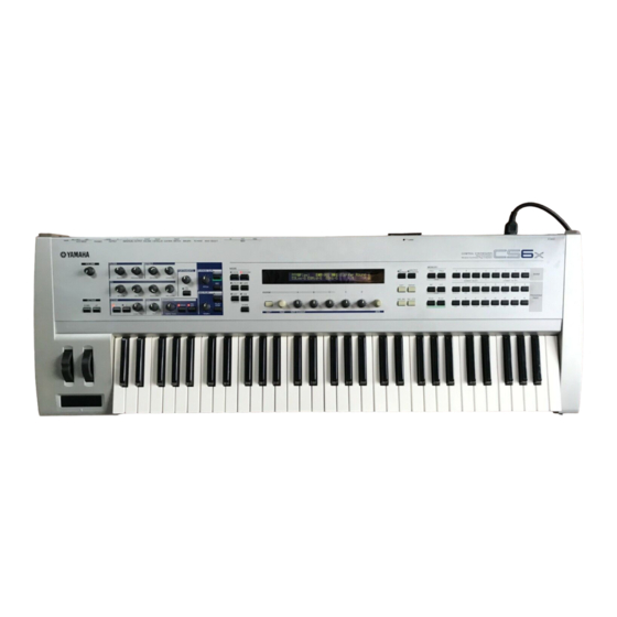
Page 4: Panel Layout
CS6X PANEL LAYOUT [VOLUME] knob OCTAVE [UP] and [DOWN] keys Front panel PITCH bend wheel MODULATION wheel Ribbon control 12 15 13 Sound Control knobs MODE keys MIC/LINE 2 LINE 1 L/MONO FOOT FOOT FOOT THRU GAIN D INPUT PHONES... -
Page 5: Circuit Board Layout
CS6X CIRCUIT BOARD LAYOUT... -
Page 6: Block Diagram
CS6X BLOCK DIAGRAM 28CA1-8813234... -
Page 7: Wiring
CS6X WIRING... -
Page 8: Disassembly Procedure
CS6X DISASSEMBLY PROCEDURE Bottom Assembly SM, RV, Display Ass'y Remove the thirty-five (35) screws marked [104], the Circuit Board & Unit Ref No. PARTS NAME PARTS No. Q'ty Fig. two (2) corner plates, marked [102], and the two (2) PLG Support Brecket Bind Head Tapping Screw-B 3.0 X 6 MFZN2BL... - Page 9 CS6X [122] [122] Fig.3 [32] [52] [42] LCD Assy [22] Fig.4 Keyboard Assembly Remove the bottom assembly. (See Procedure 1.) Remove the four(4) screws marked [72]. The keyboard Assembly can then be removed.(Fig.2)
-
Page 10: Lsi Pin Description
CS6X LSI PIN DESCRIPTION HD64F7045F28 (XW419A00) CPU NAME FUNCTION NAME FUNCTION /WRHH HH write PE14 LCD data 6 input / output Data bus /WRHL PA21 MLAN insert detect PE15 LCD data 7 input / output... - Page 11 CS6X HD63B01Y0RCE0F (XM234A00) CPU (PKS) NAME FUNCTION NAME FUNCTION /NMI Non-maskable interrupt M1/S8 Make contact of key receive/ M0/S7 Switch receive Ground Key scan drive ...
- Page 12 CS6X TC203C760HF-002 (XS725A00) SWP30B AWM Tone Generator coped with MEG) Standard Wave Processor NAME FUNCTION NAME FUNCTION (Ground) (Ground) HMD0 HMD1 HMD2 HMD3 HMD4 Address bus of internal register HMD5 HMD6 Wave memory data bus (Upper 16 bits) HMD7 HMD8...
- Page 13 CS6X MN101C027YB (XS711200) CPU NAME FUNCTION NAME FUNCTION Switch matrix data Switch matrix data MIDI transmit data VREF+ Power supply (+5V, analog) Switch matrix data Power supply (+5V) OSC2 Crystal oscillator (8MHz) OSC1 Crystal oscillator (8MHz) Ground Not used Not used...
-
Page 14: Ic Block Diagram
CS6X PCM1800 (XU770A00) A/D Converter NAME FUNCTION NAME FUNCTION VINL Analog input (L ch.) LRCK Sampling clock input/output VREF1 Reference 1 decoupling cap. Bit clock input/output REFCOM Reference decoupling common DOUT Audio data output VREF2 Reference 2 decoupling cap. SYSCK... - Page 15 CS6X TC74VHC245F(XT487A00) TC7W32FU(TE12L) (XQ173A00) TC74HC4052AF (XS790A00) TC74VHC273F(XN971A00)IC52 TC7S66FF(XR682A00) TC74HC74AF (XP003A00) IC11,IC101 SN74HC273NSR(XH223A00) IC30 IC18,IC19 IC75 IC13,IC14,IC15,IC16 Transceiver IC27, IC28,IC52 Analog Switch Dual D-Type Flip-Flop Multiplexer D-FF 1CLR IN / OUT 2CLR CLEAR OUT / IN Y-COM Y-COM COUT X-COM X-COM...
-
Page 16: Circuit Boards
CS6X CIRCUIT BOARDS DM Circuit Board CN19: to PNA-CN1 CN22: to SM-CN1 CN20: to JK-CN2 CN18: OPTION-MLAN-CN1 CN21: to JK-CN4 CN6: to RV-CN10 CN7: to PNA-CN3 CN15: to PLUG IN1-CN1 CN4: to JK-CN5 CN16: to PLUG IN2-CN1 CN13: CN12: CN14:... - Page 17 CS6X Pattern side Battery VN103500 VN103600(Battery holder for VN103500) • Notice for back-up battery removal Push the battery as shows in figure, then the battery will pop up. • Druk de batterij naar beneden zoals aangeven in de tekening, de batterij...
- Page 18 CS6X RIB Circuit Board RV Circuit Board CN15: from RIBBON CN9: to PNA-CN8 CN10: to DM-CN6 CN11: to DM-CN14 CN14: to DM-CN9 CN14: to DM-CN9 Component side Component side PNA Circuit Board CN1: CN2: CN7: CN8: to DM-CN19 to JK-CN1...
- Page 19 CS6X PNB Circuit Board CN12: to PNA-CN5 CN13: to PNA-CN6 Component side SM Circuit Board CN1: to DM-CN22 PNB: 2NA-V357980 SM: 2NA-V357710 Component side Pattern side...
- Page 20 CS6X JK Circuit Board ( B virsion) HOST SELECT INDIVIDUAL OUTPUT OUTPUT MIDI FOOT SUSTAIN FOOT FOOT INPUT PC2 PC1 to HOST BREATH GAIN SWITCH CONTROLLER VOLUME L/MONO PHONES MIC/LINE2 LINE1 THRU MIDI CN4: to DM-CN21 CN5: to DM-CN4 CN6: to PNA-CN7...
-
Page 21: Test Program
CS6X TEST PROGRAM Test No. Test Item Test Conditions, Judgment Criteria, etc. RAM READ/WRITE OK/NG, (MAIN SRAM/WAVE DRAM) RAM BATTERY OK/NG, 2.7V or more, Less than 3.5V WAVE ROM OK/NG ON/OFF blinking alternately PANEL SWITCH/LED OK/NG ENCODER OK; 0 to +127(0) to -127... - Page 22 CS6X A. HOW TO ENTER THE TEST PROGRAM C. TEST SELECTION WHEN AN ERROR HAS BEEN DETECTED While pressing the [VOICE], [PERFORM] and [STORE] When the test result has been judged as “NG” in each of switches, turn on the [POWER ON/OFF] switch. The the following tests, choose whether to execute the same following message will then appear.
- Page 23 CS6X If the wrong switch is pressed, “NG” will appear and no sine wave will be output. TEST END If the correct switch is pressed after that, testing will The test ends after the result is displayed. proceed to the next switch.
- Page 24 CS6X T7. KEYBOARD DISPLAY OF RESULTS This test is used to check that the keyboard functions (No change in the message on the display) properly by scaling 88 keys from A1 to C7. TEST END The test ends after the results have been displayed.
- Page 25 CS6X x x x: current knob value x x x: current controller value y y y: next target value y y y: next target value ZZZ: name of the Knob being checked Checking order: [ATK][DCY][SUS][REL][POR][PCH] DISPLAY OF RESULTS [SCN][PAN][ARP][TMP] DISPLAY OF RESULTS...
- Page 26 CS6X ERROR CODE T14. BREATH CONTROLLER RD/WR: read/write error NO-CARD: card is not loaded WRPRT: write protect x x x: current value of the breath controller Operate the breath controller in the following order: Not TEST END blowing (122-127) - Blowing (0-5) - Not blowing (122-127) The test ends after the result is displayed.
- Page 27 CS6X Set the master volume to Max and check that the DISPLAY OF RESULTS following signals are output from OUTPUT-L, INDIV- 1 and 2, and PHONES (L). OUTPUT-L: 1 kHz ±1.5 Hz, sine wave, +6.0 ±2 dBm (10k ohm load)
- Page 28 CS6X LINE 1, LINE 2, MIC 1 and MIC 2 can be selected by T21. A-D LEVEL, JACK using [DEC] and [INC]. With LINE 1, GAIN = LINE applies and the signal input through the A/D will be output at the D/A as is.
- Page 29 CS6X NO-BOARD: board is not loaded. DISPLAY OF RESULTS CONTROL: CONTROL line failure When the factory settings are restored TEST END When the [EXIT] switch is pressed, the sound output will stop and the next test number will be set.
- Page 30 CS6X Turn on the power while pressing [EXIT] and T28. EXIT [ENTER], and the system program will be loaded from SMART MEDIA and the operating power will be restored. When testing is executed, the following message will appear on the LCD.
- Page 31 CS6X...
- Page 32 CS6X...
- Page 33 CS6X...
- Page 34 CS6X...
- Page 35 CS6X...
- Page 36 CS6X...
- Page 37 CS6X...
- Page 38 CS6X...
- Page 39 CS6X...
-
Page 40: Midi Data Format
+--- CONTROL CHANGE Decimal Hexadecimal Binary Decimal Hexadecimal Binary MODULATION BnH,01H 0000 0000 0100 0000 PORTAMENTO TIME BnH,05H (CS6x only) 0000 0001 0100 0001 BnH,0AH (CS6x only) SUSTAIN SWITCH BnH,40H 0000 0010 0100 0010 PORTAMENTO SWITCH BnH,41H (CS6x only) 0000 0011... - Page 41 BREATH CONTROLLER SYSTEM data will be transmitted/received in all modes. FOOT CONTROLLER 4 (Transmit: CS6x and S80 only) [SW8] SYSTEM Bank Select Switch SCENE CONTROL 14 (Transmit/Receive: CS6x only) [SW9] SYSTEM Program Change Switch (Received only in the Play Mode when Voice Mode or KNOB 1 Phrase Clip Mode is selected.)
- Page 42 (3-6-1-2)IDENTITY REQUEST(Receive only) ank Select will be actually executed when the Program Change message is received. ank Select and Program Change numbers that are not supported by Yamaha will be gnored. F0H 7EH 0nH 06H 01H F7H ("n" = Device No.However, this instrument receives under "omni.")
- Page 43 CS6X HOST MODE = MIDI To Host From Host Local Sw MIDI Out MIDI In HOST MODE = PC1/PC2/MAC To Host From Host Local Sw MIDI Out MIDI In Although three types of note on/note off data, received via MIDI, played by the internal sequencer and played on the keyboard will be distinguished, the other controllers (channel messages) equally affect the entire notes.
- Page 44 CS6X...
- Page 45 CS6X...
-
Page 46: Parts List
PARTS LIST CONTENTS OVERALL ASSEMBLY ..........2 PANEL ASSEMBLY ......... 4 WHEEL ASSEMBLY ........5 MK ASSEMBLY ............ 6 POWER SUPPLY ASSEMBLY ......7 ELECTRICAL PARTS ..........8 Notes : DESTINATION ABBREVIATIONS A : Australian model M : South African model B : British model O : Chinese model C : Canadian model... - Page 47 CS6X OVERALL ASSEMBLY Panel Assembly (See page 4) Wheel Assembly (See page 5) 110b 110a Power Supply Assembly (See page 7) MK Assembly (See page 6) 100a 100d 100b 100c...
- Page 48 CS6X PART NO. DESCRIPTION REMARKS PART NO. DESCRIPTION REMARKS REF NO. RANK REF NO. RANK OVERALL ASSEMBLY CS6X VP204400 AC Cord BS 3 Overall Assembly (V387080) VQ240200 Adapter, AC Cord KPR-24 Overall Assembly (V387090) CD-ROM 74min. 12cm (XW444B00) Overall Assembly...
-
Page 49: Ep600230 4
CS6X PANEL ASSEMBLY PART NO. DESCRIPTION REMARKS REF NO. RANK PANEL ASSEMBLY CS6X Panel Assembly (V387110) Control Panel (V387190) V 3 2 7 2 3 0 0 Cover (S) VS863000 Flat Head Screw 3.0X6 MFZN2BL Display Assembly (V387150) EP600230 Bind Head Tapping Screw-B 3.0X6 MFZN2BL... - Page 50 CS6X WHEEL ASSEMBLY PART NO. DESCRIPTION REMARKS REF NO. RANK WHEEL ASSEMBLY CS6X Wheel Assembly (V387160) VF 5 3 6 8 0 0 Frame VQ546400 Wheel V 4 5 7 9 9 0 0 Wheel Since 1999,11,01 VC792800 Spring CB819020...
- Page 51 CS6X MK ASSEMBLY PART NO. DESCRIPTION REMARKS REF NO. RANK MK ASSEMBLY CS6X MK Assembly (V441400) VN399200 Keyboard Assembly C61K6 Front Rail (V410720) EP600230 Bind Head Tapping Screw-B 3.0X6 MFZN2BL VN399200 Keyboard Assembly C61K6 VN405500 MK Frame Assembly LC C61...
- Page 52 CS6X POWER SUPPLY ASSEMBLY PART NO. DESCRIPTION REMARKS REF NO. RANK POWER SUPPLY ASSEMBLY CS6X Power Supply Assembly (V387130) Power Supply Assembly (V387140) Shield Plate (V474280) V 3 4 8 4 1 0 0 Power Supply Unit J,U,C V 3 4 8 4 2 0 0...
- Page 53 CS6X ELECTRICAL PARTS PART NO. DESCRIPTION REMARKS REF NO. RANK ELECTRICAL PARTS CS6X V 3 5 7 9 1 0 0 Circuit Board (XV911B0) V 3 5 7 9 9 0 0 Circuit Board (XV914C0) V I 9 1 2 0 0 0...
- Page 54 CS6X PART NO. DESCRIPTION REMARKS REF NO. RANK IC10 XM234A00 HD63B01Y0RCE0F IC11 XT487A00 TC74VHC245F TRANSCEIVER IC12 XV103A00 M5M34051FP LINE TRANSCEIVER IC13 XS790A00 TC74HC4052AF XS790A00 TC74HC4052AF IC17 XD657A00 TC74HC14AF-TP1 INVERTER IC18 XP003A00 TC74HC74AF D-FF IC19 TC74HC74AF D-FF XP003A00 IC20 XD657A00 TC74HC14AF-TP1...
- Page 55 CS6X PART NO. DESCRIPTION REMARKS REF NO. RANK RA30 RE044680 Resistor Array 68X4 RA31 RE047100 Resistor Array 10KX4 RE047100 Resistor Array 10KX4 RA34 RE047150 Resistor Array 15KX4 RA35 RE047150 Resistor Array 15KX4 RA36 RE047220 Resistor Array 22KX4 RA37 RE047220 Resistor Array...
- Page 56 CS6X PART NO. DESCRIPTION REMARKS REF NO. RANK 316,329-332 UF037470 Electrolytic Cap. (chip) 47 16V C:24,41,44,167,247,249, 250,267,269,270,605 UF038100 Electrolytic Cap. (chip) 100 16V C:219 UF046470 Electrolytic Cap. (chip) 4.7 25V C:285,286,323 UF066100 Electrolytic Cap. (chip) 1 50V C:32 UF066330 Electrolytic Cap. (chip) 3.3 50V...
- Page 57 CS6X PART NO. DESCRIPTION REMARKS REF NO. RANK Angle JKAD (V388510) Angle JKBC (V388520) VU931500 Holder, Jack V 2 1 9 2 7 0 0 VR Shield CB069250 Cord Holder BK-1 VA078900 Jumper Wire 0.55 VB390100 Connector Base Post PH-5P TE...
- Page 58 CS6X PART NO. DESCRIPTION REMARKS REF NO. RANK HF454560 Carbon Resistor 56.0 1/4 J R:59,60 HF455100 Carbon Resistor 100.0 1/4 J R:7,16,19,27,35,43,52,80, 83,90,91 HF455220 Carbon Resistor 220.0 1/4 J R:5,14,69,72 HF455470 Carbon Resistor 470.0 1/4 J R:75 HF456100 Carbon Resistor 1.0K 1/4 J...
- Page 59 CS6X PART NO. DESCRIPTION REMARKS REF NO. RANK VA078900 Jumper Wire 0.55 VA078900 Jumper Wire 0.55 VA078900 Jumper Wire 0.55 VA078900 Jumper Wire 0.55 VS704700 SEL2210W TP8 RE SCENE(1,2),PORT ON/OFF, VS704700 SEL2210W TP8 RE ARP.(HOLD,ON/OFF), PHASE CLIP,SEQ PLAY, VOICE PERFORM,UTILITY,...
- Page 60 CS6X CIRCUIT DIAGRAM 1/4 ( DM1/3 ) CS6X to SV-CN3 to JK-CN5 to PS-CN3 INVERTER to JK-CN7 to RV-CN5 to WHEEL PHOTOCOUPLER to RIBBON LINE KEYBOARD TRANSCEIVER CN1,CN3 OP AMP KEYBOARD CN2,CN4 to LC KEYBOARD INVERTER INVERTER INVERTER D-FF to RV-CN6...
- Page 63 CS6X CIRCUIT DIAGRAM 4/4 ( PNA , PNB , JK , RIB ) CS6X to JK-CN6 RIBBON to DM-CN9 to DM -CN17 to DM -CN19 to JK -CN1 to DM-CN22 28CC1-8813231 OPAMP PHONES OPAMP OPAMP GAIN to DM-CN4 to DM-...