Aiwa XR–DV525 Service Manual
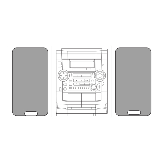
Dvd stereo system aiwa xr–dv525
Hide thumbs
Also See for XR–DV525:
- Service manual (44 pages) ,
- Operating instructions manual (56 pages)
Table of Contents
Advertisement
SERVICE MANUAL
DVD STEREO SYSTEM
SYSTEM
XR–DV525
• This Service Manual is the "Revision Publishing" and replaces "Simple Manual"
(S/M Code No. 09-007-434-1T3).
• If requiring information about the DVD mechanism, see Service Manual of AZG-D,
(S/M Code No. 09-00A-350-6N2).
XR-DV525
BASIC TAPE MECHANISM : 2ZM-3MK2 PR9NM
BASIC DVD MECHANISM : AZG-D ZACPDM
CD
CASSEIVER
CX–NDV525
S/M Code No. 09-00C-434-1R3
SPEAKERS
CONTROLLER
SX–NDV824
RC–AAS03
SX–CR677
HR, HT
REMOTE
Advertisement
Table of Contents

Related Manuals for Aiwa XR–DV525


Summary of Contents for Aiwa XR–DV525
- Page 1 XR-DV525 HR, HT SERVICE MANUAL BASIC TAPE MECHANISM : 2ZM-3MK2 PR9NM DVD STEREO SYSTEM BASIC DVD MECHANISM : AZG-D ZACPDM REMOTE SYSTEM SPEAKERS CASSEIVER CONTROLLER SX–NDV824 XR–DV525 CX–NDV525 RC–AAS03 SX–CR677 • This Service Manual is the “Revision Publishing” and replaces “Simple Manual” (S/M Code No.
-
Page 2: Specifications
SPECIFICATIONS Main unit CX-NDV525 Supported discs DVD video discs 12 cm (single-sided single-layer, single- <FM Tuner section> sided double-layer, double-sided-double Tuning range 87.5 MHz to 108 MHz layer) Usable sensitivity (IHF) 13.2 dBf 8 cm (single-sided single-layer, single- Antenna terminals 75 ohms (unbalanced) sided double-layer, double-sided-double layer) -
Page 3: Protection Of Eyes From Laser Beam During Servicing
PROTECTION OF EYES FROM LASER BEAM DURING SERVICING CAUTION This set employs laser. Therefore, be sure to follow carefully the instructions below when servicing. Use of controls or adjustments or performance of proce- dures other than those specified herin may result in WARNING!! hazardous radiation exposure. -
Page 4: Note On Before Starting Repair
NOTE ON BEFORE STARTING REPAIR 1. Forced discharge of electrolytic capacitor of power supply block When repair is going to be attempted in the set that uses relay circuit in the power supply block, electric potential is kept charged across the electrolytic capacitors (C101, 102) even though AC power cord is removed. - Page 5 In such a case, check also if the POWER AMPLIFIER circuit or power supply circuit has any abnormalities or not. 2-2. Regarding reset There are cases that the machine does not work correctly because the MICROCOMPUTER is not reset even though the AC power cord is re-inserted, or the software reset (pressing the STOP key + POWER key) is performed.
-
Page 6: Electrical Main Parts List
ELECTRICAL MAIN PARTS LIST REF. NO. PART NO. KANRI DESCRIPTION REF. NO. PART NO. KANRI DESCRIPTION 87-010-406-080 CAP,ELECT 22-50 87-010-406-080 CAP,ELECT 22-50 87-A21-269-010 IC,EW732 87-010-263-080 CAP,ELECT 100-10V 87-A21-355-010 IC,STK490-140 87-010-197-080 CAP,CHIP 0.01 DM 8A-DJV-613-030 C-IC,LC876572V-5T19 87-010-260-080 CAP,ELECT 47-25V 87-A21-629-010 IC,SPS-442-1-N 87-A20-783-040 C-IC,BA7762AFS 87-010-380-080... - Page 7 REF. NO. PART NO. KANRI DESCRIPTION REF. NO. PART NO. KANRI DESCRIPTION C394 87-010-319-080 C-CAP,S 56P-50 CH C624 87-010-401-080 CAP,ELECT 1-50V C401 87-010-176-080 C-CAP,S 680P-50 SL C626 87-010-596-080 C-CAP,S 0.047-16 C402 87-010-176-080 C-CAP,S 680P-50 SL C627 87-010-400-080 CAP,ELECT 0.47-50V C403 87-010-958-080 CHIP-CAP,S 0.01-25BJ C628...
- Page 8 REF. NO. PART NO. KANRI DESCRIPTION REF. NO. PART NO. KANRI DESCRIPTION C848 87-010-197-080 CAP,CHIP 0.01 DM L801 87-A50-608-010 COIL,FM DET-N(TOK) C849 87-010-197-080 CAP,CHIP 0.01 DM L802 87-A91-552-010 FLTR,CFMT-450AL(TOK) C850 87-010-260-080 CAP,ELECT 47-25V L811 87-005-847-080 COIL,2.2UHK CECS C851 87-010-197-080 CAP,CHIP 0.01 DM L832 87-005-847-080 COIL,2.2UHK CECS...
- Page 9 REF. NO. PART NO. KANRI DESCRIPTION REF. NO. PART NO. KANRI DESCRIPTION C401 87-010-197-080 CAP,CHIP 0.01 DM SW252 87-A91-555-010 SW,RTRY EC12E24504 C451 87-010-196-080 CHIP CAPACITOR,0.1-25 SW253 87-A91-542-010 SW,RTRY EC12E12504 C452 87-010-196-080 CHIP CAPACITOR,0.1-25 C453 87-010-196-080 CHIP CAPACITOR,0.1-25 C454 87-010-198-080 CAP,CHIP 0.022 AMP 1F C.B C455 87-010-198-080...
- Page 10 REF. NO. PART NO. KANRI DESCRIPTION REF. NO. PART NO. KANRI DESCRIPTION 87-A11-148-080 CAP,TC U 0.1-50 Z F DECK C.B 87-A11-148-080 CAP,TC U 0.1-50 Z F 87-010-403-080 CAP,ELECT 3.3-50V CON1 87-099-756-010 CONN,15P 9604S F 87-016-657-090 CAP,E 3300-71 M SMG 87-045-347-010 MOT,SHU2L 70 87-016-657-090 CAP,E 3300-71 M SMG...
-
Page 11: Transistor Illustration
TRANSISTOR ILLUSTRATION E C B E C B E C B B C E CD1585 2SA1981 2SB1370 2SA933 CSC4115 2SC1740 KTA1266 DTC114ES KTC3198 KTC3199 2SA1235 DTC144EK 2SK2158 2SK360 2SC2714 KRA102S 2SC3052 KRA107S CMBT5401 RT1N141C CMBT5551 RT1P141C CSD1306 RT1P441C – 11 –... - Page 12 BLOCK DIAGRAM – 1 (MAIN UNIT / DVD UNIT) – 12 –...
- Page 13 BLOCK DIAGRAM – 2 (MAIN / FRONT / AMP 1F / PT / P– LOG / DECK) – 13 –...
- Page 14 WIRING – 1 (MAIN / VM3) – 14 –...
- Page 15 SCHEMATIC DIAGRAM – 1 (MAIN : 1 / 4 / VM3) – 15 –...
- Page 16 SCHEMATIC DIAGRAM – 2 (MAIN : 2 / 4 <TUNER SECTION>) – 16 –...
- Page 17 SCHEMATIC DIAGRAM – 3 (MAIN : 3 / 4 <DECK SECTION> / HEAD – 1 / HEAD – 2) – 17 –...
- Page 18 SCHEMATIC DIAGRAM – 4 (MAIN : 4 / 4 <PRO LOGIC SECTION>) – 18 –...
-
Page 19: Wiring - 2 (Front)
WIRING – 2 (FRONT) – 19 –... - Page 20 SCHEMATIC DIAGRAM – 5 (FRONT / DECK) – 20 –...
- Page 21 WIRING – 3 (AMP 1F) – 21 –...
- Page 22 SCHEMATIC DIAGRAM – 6 (AMP 1F) – 22 –...
- Page 23 WIRING – 4 (PT) – 23 –...
-
Page 24: Schematic Diagram - 7 (Pt)
SCHEMATIC DIAGRAM – 7 (PT) – 24 –... - Page 25 WIRING – 5 (P – LOG) – 25 –...
- Page 26 SCHEMATIC DIAGRAM – 8 (P–LOG) – 26 –...
- Page 27 WIRING – 6 (DECK / HEAD – 1 / HEAD – 2) – 27 –...
- Page 28 FL (HNA – 11MM34) GRID ASSIGNMENT / ANODE CONNECTION / PIN CONNECTION GRID ASSIGNMENT ANODE CONNECTION PIN CONNECTION – 28 –...
-
Page 29: Ic Block Diagram
IC BLOCK DIAGRAM – 29 –... - Page 30 – 30 –...
- Page 31 IC DESCRIPTION IC, LC876572V-5T19 Pin No. Pin Name Description I-STEREO Tuner stereo signal input. I-IFC Tuner IF count serial data input. – Not connected. O-POWER Power ON/OFF output. I-HP-MUTE Headphone insert detection input. O-DATA(M) IC control serial data output. O-STB(M) Main strobe output.
- Page 32 Pin No. Pin Name Description P21 / RDS FL segment output / RDS initial diode setting input (not used). P20 / FM1 FL segment output / FM1 initial diode setting input (not used). P19 / SW FL segment output / SW initial diode setting input. P18 / LW FL segment output / LW initial diode setting input (not used).
- Page 33 IC, LC72131D Pin No. Pin Name Description X-IN A crystal oscillator (4.5MHz) is connected between these pins. X-OUT – Not connected. To enable the IC. Active "H". Digital data input from CPU (LC876572V-5T19) when relevant key is operated. Active "H". To clock in the data DI.
- Page 34 ADJUSTMENT – 1 <TUNER / FRONT> < TUNER SECTION > 1. Clock Frequency Check 9. DC Balance / Mono Distortion Adjustment Settings : • Test point : TP2 (CLK) Settings : • Test point : TP3, TP4 (DC) Method : Set to MW 1602kHz and check that the test point is •...
- Page 35 ADJUSTMENT – 2 <DECK> < DECK SECTION > 1. Tape Speed Adjustment (DECK 2) 5. REC/PB Frequency Response Adjustment (DECK 2) Settings : • Test tape : TTA–100 Settings : • Test tape : TTA–602 • Test point : TP8 (Lch), TP9 (Rch) •...
-
Page 36: Dvd Test Mode
DVD TEST MODE 1. How to Activate DVD Test Mode Insert the AC plug, while pressing the DVD/CD/VCD function button. All the indicators on the FL display tube will light up, and the test mode will be activated. 2. How to Cancel DVD Test Mode Either one of the following operations will cancel the DVD test mode. -
Page 37: Mechanical Exploded View
MECHANICAL EXPLODED VIEW 1 / 1 AZG-D ZACPDM FL401 HT-SINK,T5A HT-SINK VM2 PLATE,PT 25 26 PLATE,EARTH MIC 30 31 CHAS,MAIN 2ZM-3MK2 PR9NM PLATE,EARTH MECH – 37 –... -
Page 38: Mechanical Parts List
13 8A-DJV-017-010 PANEL,FR H 48 8Z-NB8-254-010 COVER, PL M3 14 8A-DJV-009-010 WINDOW,DISP H 49 87-085-221-010 FOOT,H13.5 15 87-CE3-023-010 BADGE,AIWA 30N SILV 50 87-085-185-010 BUSHING, AC CORD (E) 16 8A-DJV-034-010 PANEL,CD 51 87-A80-157-010 AC CORD ASSY,E BLK CC 17 8A-DJV-003-010 CABI,STEEEL... -
Page 39: Tape Mechanism Exploded View
TAPE MECHANISM EXPLODED VIEW 1 / 1 PLATE SHLD,M3 GEAR PLAY GEAR PLAY PLATE SHLD,M3 – 39 –... -
Page 40: Tape Mechanism Parts List
TAPE MECHANISM PARTS LIST 1 / 1 REF. NO. PART NO. KANRI DESCRIPTION REF. NO. PART NO. KANRI DESCRIPTION 1 82-ZM3-335-310 PULLEY,COUPLER M3 36 82-ZM3-340-010 SH,BELT D2 2 87-B10-043-010 W-P,0.99-4-0.25 SLT 37 82-ZM1-242-010 LVR,CAS 3 86-ZM1-206-010 BELT,MAIN L 38 82-ZM3-329-410 BELT,SBU R2 4 82-ZM1-322-010 SPR-T,FR 60... -
Page 41: General Speaker Disassembly Instructions (For Reference)
GENERAL SPEAKER DISASSEMBLY INSTRUCTIONS (FOR REFERENCE) Type.1 Type.4 Insert a flat-bladed screwdriver into the position indicated by the TOOLS arrows and remove the panel. Remove the screws of each speaker 1 Plastic head hammer unit and then remove the speaker units. 2 (() flat head screwdriver 3 Cut chisel How to Remove the PANEL, FR... -
Page 42: Accessories / Package List
SPEAKER PARTS LIST (SX–NDV824) <Y1BL, YJBL, YJ7BL> REF. NO. PART NO. KANRI DESCRIPTION 1 8A-NSV-001-010 PANEL,FR R 2 8A-NSV-002-010 PANEL,FR L 3 8A-NSV-004-010 GRILLE,FRAME ASSY R 4 8A-NSV-008-010 GRILLE,FRAME ASSY L 5 87-NSS-602-010 SPKR,W 160 6 88-SSM-603-010 SPKR,TW 60 7 8A-NSV-012-010 PROTECTOR,TW 8 8Z-CL5-543-010 CORD,SP... - Page 43 2–11, IKENOHATA 1–CHOME, TAITO-KU, TOKYO 110, JAPAN TEL:03 (3827) 3111 9420025 0251431 Printed in Singapore...
Need help?
Do you have a question about the XR–DV525 and is the answer not in the manual?
Questions and answers