Table of Contents
Advertisement
Advertisement
Table of Contents

Related Manuals for Lucky Star 5MVP3


Summary of Contents for Lucky Star 5MVP3
- Page 1 5MVP3 Ver.4.0 AT Form Factor Main Board User's Manual...
- Page 2 Copyright Copyright © 1998 by this company. No part of this document may be reproduced, transmitted, transcribed, stored in a retrieval system, or translated into any language or computer language, in any form or by any means without prior written permission. This manual and the information contained herein are protected by copyright.
- Page 3 Warning and disclaimer This manual is designed to provide information about Pentium® system board. Every effort has been made to make this manual as accurate as possible, but no warranty or fitness is implied. All the information is provided on an 'as is' basis. The author and his corresponding publishing company shall have neither liability nor responsibility to any person or entity with respect to any loss or damages arising from the information contained in this manual or...
-
Page 4: Table Of Contents
Table of contents Chapter 1 Introduction _______________________ Main Board Overview____________________________________1 Specifications__________________________________________3 Notice of Hardware Installation_____________________________5 Chapter 2 Installation_________________________ Layout Reference________________________________________7 Quick reference to CPU Speed Setup_________________________8 Jumper Settings________________________________________ 10 2-3-1 S1_____________________________________________10 2-3-2 S2_____________________________________________12 2-3-3 JP4 DIMM Voltage Selector________________________13 2-3-4 JP5 Flash ROM Voltage Selector____________________14 2-3-5 JP7 CMOS Status________________________________15 Connectors___________________________________________ 16 2-4-1 CN10 Front Panel Connectors_______________________16... - Page 5 Chapter 3 BIOS Setup________________________ Award BIOS CMOS Setup________________________________33 Standard CMOS Setup___________________________________ 34 BIOS Features Setup____________________________________ 36 Chipset Features Setup___________________________________40 Power Management Setup________________________________ 42 PNP/PCI Configuration Setup_____________________________ 45 Integrated Peripherals____________________________________47 Supervisor/ser Password_________________________________ 50 IDE HDD Auto Detection________________________________ 53 3-10 Load Setup Defaults_____________________________________56 3-11 Save and Exit Setup_____________________________________.57 3-12 Quit Without Saving____________________________________ 58 Chapter 4 Appendix__________________________...
-
Page 6: Chapter 1 Introduction
Chapter 1 Introduction 1-1 Main Board Overview The main board is a new-generation AGP Pentium® main board with high performance in rendering and texture for 3D Graphics. Based on Apollo MVP3 chipset, the main board has intergrated the latest advances in processor, memory, I/O technologies into an AT form factor. - Page 7 The main board is also strengthened with Power Management Wake up Event such as “WOL (Wake up on LAN),” and “Modem ring on,” which are the new inventions to enable PCs to be turned on over the network or modem. These are also key benefits in PC operation, asset management, new system setup and power conservation.
-
Page 8: Specifications
1-2 Specifications ● PCB board size: 25 cm x 22 cm ● PCB layer: 4 layers ● ZIF Socket 7 Support Intel® Pentium, Cyrix 6x86 series/ MII series, IDT WinChip series and AMD K5/K6/K6-2/K6-III CPUs CPU is not enclosed in the package ●... - Page 9 ● I/O function ! ! ! ! 2 x PCI IDE devices ! ! ! ! 1 x FDC, 2 x serial ports(16550 fast com) ! ! ! ! 1x parallel port device /EPP/ECP ! ! ! ! 2x USB connector ! ! ! ! IrDA (infrared) connector ●...
-
Page 10: Notice Of Hardware Installation
1-3 Notice of Hardware Installation Before hardware installation, make sure you have checked the following things. A. Check the package If any of these items is missing or damaged, contact the dealer from whom you purchase. Leave this main board in its original package until you are ready to install it. - Page 11 MVP3 Main Board...
-
Page 12: Chapter 2 Installation
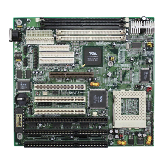
Chapter 2 Installation 2-1 Layout Reference U SB K /B B IO S M O U SE C O M 2 L PT C N 5 C O M 1 C N 6 L A N FD C SL 3 SL 2 SL 1 PC I3 PC I2 PC I1 ID E 2 ID E 1... -
Page 13: Quick Reference To Cpu Speed Setup
2-2 Quick Reference to CPU Speed Setup The setup of CPU speed is simplied to a “DIP switch form,” which is only related to jumpers S1 and S2. This design is also convenient to recognize those jumpers as below. S2: CPU voltage selector MVP3 Main Board... - Page 14 Intel Pentium PU SYS. Ratio Clock Clock Voltage P54C 100 MHZ 66 MHZ 3.3V 1.5X P54C 120 MHZ 60 MHZ 3.3V P54C 133 MHZ 66 MHZ 3.3V P54C 150 MHZ 60 MHZ 3.3V 2.5X P54C 166 MHZ 66 MHZ 3.3V 2.5X P55C 166 MHZ 66 MHZ 2.8/3.3V 2.5X...
-
Page 15: Jumper Settings
2-3 Jumper Settings With a careful design for the CPU speed jumper, this main board has been simplied to a “DIP Switch” form. It is very convenient to set CPU speed under DIP switch. 2-3-1 S1 S1 Pin 1 to Pin 3: CPU Ratio Selector CPU Ratio Pin 1 Pin 2... - Page 16 S1 Pin 4 to Pin 6: CPU Frequency Selector CPU Frequency Pin 4 Pin 5 Pin 6 60 MHz 66.6 MHz 75 MHz 83.3 MHz 95 MHz 100 MHz S1 Pin 7: SDRAM Clock Frequency S1 Pin 7 SDRAM Clock Freq. SDRAM clock is fixed on 66 MHz SDRAM Clock is the same with CPU clock MVP3 Main Board...
- Page 17 2-3-2 S2 CPU Voltage Selector S2: CPU voltage selector CPU Vcore Pin 1 Pin 2 Pin 3 Pin 4 2.1V 2.2V 2.4V 2.7V 2.8V 2.9V 3.2V 3.3V 3.5V MVP3 Main Board...
-
Page 18: Jp4 Dimm Voltage Selector
2-3-3 JP4 DIMM Voltage Selector JP4 is a 4-pin connector to select either 3.3V or 5V DIMM voltage. Select “1-2, 3-4” for 5V DIMM, or “5-6, 7-8” for 3.3V DIMM.. JP4: DIMM voltage selector DIMM Voltage 1-2, 3-4 5-6, 7-8 3.3V MVP3 Main Board... -
Page 19: Jp5 Flash Rom Voltage Selector
2-3-4 JP5 Flash ROM Voltage Selector JP5 is a 3-pin connector to select 5V or 12V flash ROM. Select “1-2” for 5V or “2-3” for 12V. JP5: Flash ROM voltage selector Pin1 Flash ROM Voltage MVP3 Main Board... -
Page 20: Jp7 Cmos Status
2-3-5 JP7 CMOS Status----clearing content of CMOS JP7: CMOS status Pin1 JP7 is a 3-pin connector. Clear CMOS if system password is forgotten. Below is details to show how to clear CMOS. CMOS Status Normal Clear CMOS Procedure to clear CMOS: Step 1: Shut down the system and disconnect the power supply from AC power. -
Page 21: Connectors
2-4 Connectors There are many connectors on this main board. Refer to the following pages for details. 2-4-1 CN10 Front Panel Connectors Front panel has connectors as “HDD-LED,” “SOFT-PWR,” “TB-LED,” “SPEAKER,” “KEYLOCK,” and “POWER-LED.” Refer to details as below. CN10: Front Panel RESET HDD-LED SPEAKER POWER LED... - Page 22 SMI connector is a 2-pin Berg strip, which is also called “green” or “sleep” connector. When SMI is turned from open to close and back to open, the system will enter sleep mode immediately. This function is to make sure power saving is working well.
-
Page 23: Back Panel Connectors
2-4-2 Back Panel Connectors There are COM1/ COM2, LPT, USB and keyboard/ mouse on case back panel. Please refer to more details as below. COM1/COM2 The onboard serial port 1 and port 2 are the 9-pin D-subminature male connector COM1 and COM2. COM1 and COM2 can be disabled in BIOS setup. -
Page 24: Lpt Parallel Port
LPT Parallel Port The onboard parallel port is a 25-pin female connector, marked as “LPT.” LPT: Parallel port Signal Signal Pin 1 Strobe Pin 14 Auto feed Pin 2 Data bit 0 Pin 15 Error Pin 3 Data bit 1 Pin 16 Init Pin 4 Data bit 2 Pin 17 SLCT in... -
Page 25: Cn8 Usb
CN8 USB (Universal Serial Bus) Universal Serial Bus connector, marked “USB,” is used to connect USB devices. There are 2 USB connectors on this main board. Keyboard The onboard PS/2 keyboard and mouse connector is 6-pin Mini-Din connectors, marked “KB.” KB: Keyboard connector Description Pin 1 Data signal... -
Page 26: Cn4 Mouse
CN4 Mouse CN4 is a 4-pin connector to connect to mouse connector. CN4: PS/2 mouse Pin1 MVP3 Main Board... -
Page 27: Cn5 Atx Power Supply Connector
2-4-3 CN5 ATX Power Supply Connector ATX power supply connector has 20 pins, which is designed for ATX case especially. The ATX power supply supports the function of the “Soft Power On Momentary switch” which connects on the front panel switch to the 2-pin SOFT-PWR on the system board. -
Page 28: Cn7 At Power Supply Connector
2-4-4 CN7 AT Power Supply Connector CN7: AT power connector Signal Signal POWER GOOD GROUND +5V DC GROUND +12V DC -5V DC -12V +5V DC GROUND +5V DC GROUND +5V DC MVP3 Main Board... -
Page 29: Cn8 Ir Connector
2-4-5 CN8 IR Connector IR connector supports wireless infrared module. With this module and application software like LAPlink, or WIN95 Direct Cable Connection, user can transfer data to or from laptops, notebooks, PDA and printers. This connector supports HPSIR, ASKIR, and Fast IR. Attach Infrared module to IR connector and enable BIOS “Infrared function.”... -
Page 30: Fan1/Fan2 Connectors
2-4-6 FAN1 /FAN2 Connectors There are 2 fan connectors on 5MVP3, and they are marked as “FAN 1,” and “FAN2.” Each fan connector has three pins. Fan Signal Ground +12V Sense FAN2 FAN1 MVP3 Main Board... -
Page 31: Fdc Floppy Interface
2-4-7 FDC Floppy Interface Floppy interface connector with 34 pins is used to attach the floppy drive cable. FDC: Floppy disk connector Signal Signal Pin 1 Data rate selection Pin 3 Pin 5 Pin 7 FDC index Pin 9 FDD Motor A enable Pin 11 GND FDD Drive B enable Pin 13 GND... -
Page 32: Ide1 And Ide2 Ports
2-4-8 IDE 1 and IDE2 IDE 1/ IDE 2 both have 40 pins. There are 2 IDE connectors supported on this system board. IDE1 is primary channel, and IDE2 is secondary channel. Each channel supports 2 IDE devices, and 4 channels in total for this main board. IDE2 IDE1 Signal... -
Page 33: Lan
2-4-9 LAN Wake up on LAN, marked as “LAN,” is a 3-pin connector. To support this feature, a network card is required for the system. More than that, a network management software must be installed too. WOL: Wake up on LAN Wake up on LAN function requirement: Power should offer at least 750mA to the signal “5V trickle voltage”... -
Page 34: Expansion Slot
2-5 Expansion Slots Expansion slots contain one A.G.P slot, three PCI slots, and three ISA slots on this main board. Below are details. Expansion S lots ISA Slots PCI Slots MVP3 Main Board... - Page 35 AGP (Accelerated Graphic Port) is the new bus standard that allows the bus speed to run at 66 MHz with up to 133 MHz data transfer capabilities, which is four times as fast as that of the PCI bus. At this speed, the AGP graphic cards can transfer data up to 528MB/second.
-
Page 36: Dimm Memory Installation
2-6 DIMM Memory Installation 5MVP3 has 3 DIMMs on board. Either DIMM 1, DIMM2, or DIMM3 supports 8 MB, 16 MB, 32 MB, 64 MB, and 128MB. Maximum memory for SDRAM is up to 384MB; EDO RAM is up to 768 MB. This main board also supports asynchronous operation for CPU and DIMM data transfer. - Page 37 Insert the module as shown. Due to different number of pins on either side of the breaks, the module will only fit in the orientation as shown. DIMM MVP3 Main Board...
-
Page 38: Chapter 3 Bios Setup
Chapter 3 BIOS Setup 3-1 Award BIOS CMOS Setup The menu displays all the major selection items and allow user to select any of shown item. The selection is made by moving cursor (press any direction key ) to the item and press <Enter> key. An on-line help message is displayed at the bottom of the screen as cursor is moving to various items which provides user better understanding of each function. -
Page 39: Standard Cmos Setup
3-2 Standard CMOS Setup The ”Standard CMOS Setup” allows user to configure system setting such as current date and time, type of hard disk drive installed in the system, floppy drive type, and the type of display monitor. Memory size is auto detected by the BIOS and displayed for your reference. - Page 40 Hard Disk Configurations 1. TYPE : select from "1" to "45" to fill remaining fields with redefined values of disk drives. Select "USER" to fill the remaining fields. Select "AUTO" to detect the HDD type automatically. 2. SIZE : the hard disk size. The unit is mega byte(MB). 3.
-
Page 41: Bios Features Setup
5MVP3 3-3 BIOS Features Setup Menu below shows all of the manufacturer's default values of this main board. Move the cursor by pressing direction keys and <PageDown> or <PageUp> key to modify the parameters, pressing [F1] key to display help message of the selected item. - Page 42 5MVP3 External Cache Enabled (default): enable L2 cache Disabled: disable L2 cache Quick Power On Self Test This category speeds up power on self test. Enabled : BIOS will shorten or skip some check items. Disabled: normal speed Boot sequence This category determines which drive the system searches first.
- Page 43 5MVP3 Typematic Rate Setting This determines the typematic rate. Enabled: enable typematic rate and typematic delay programming. Disabled (default): disable typematic rate and typematic delay programming. The system bios will use default value of this 2 items and the default is controlled by keyboard.
- Page 44 5MVP3 OS Select For DRAM> 64MB This option is especially set for OS2 operating system. Set “Non-OS2” for RAM memory over 64MB and set “Non-OS2” for other operating systems like Windows® 95/98 or NT. Non-OS2 (default) Video BIOS Shadow It determines whether video BIOS will be copied to RAM. However, it is optional from chipset design.
-
Page 45: Chipset Features Setup
5MVP3 3-4 Chipset Features Setup Bank 0/1(2/3, 4/5) DRAM Timing This will determine the timing of SDRAM. The user can separately adjust the timing of bank 0/1, 2/3, 4/5. : FP/EDO 70ns (default) : FP/EDO 70ns, Normal, Medium, Fast, Turbo SDRAM Cycle Length: control the DRAM page missing and row miss leadoff timing. - Page 46 5MVP3 Memory Hole at 15Mb Addr.: this field enable a memory hole in main memory space. CPU cycles matching an enabled hole are passed on to PCI bus. :Disabled (default) :15M-16M AGP Aperture Size To select the size of the Accelerated Graphics Port (AGP) aperture is a portion of the PCI memory address range dedicated for graphics memory address space.
-
Page 47: Power Management Setup
5MVP3 3-5 Power Management Setup ACPI function :Disabled (default) :Enabled Power Management :User Define(default)--users can configure their own power management :Min Saving :Max Saving :Disabled MVP3 Main Board... - Page 48 5MVP3 PM Control By APM No : system BIOS will ignore APM. Yes (default) : system BIOS will wait for APM's prompt before it enter any PM mode, e.g. Doze, standby or suspend. Note 1: if APM is installed, and there is a task running, even if the timer...
- Page 49 5MVP3 Modem Ring Resume Enabled: modem ring on function--- system can be turned on through modem. Disable (default): disble this function Note: this function only works when the system is turned off from Windows mode, and Doze mode will not function.
-
Page 50: Pnp/Pci Configuration Setup
5MVP3 PNP / PCI Configuration Setup PNP OS Installed :No(default) OS will not recognize PnP devices. :Yes OS will arrange the setup of PnP devices. Resources Controlled By :Manual(default) The table will show the below items: “Reset Configuration Data, IRQ-3 assigned to, DMA-0 assigned to.”... - Page 51 5MVP3 Reset Configuration Data :Disabled(default) :Enabled--- to reset “Extended System Configuration Data(ESCD) when you exit setup if you have installed a new add-on card and the system reconfiguration has caused such a serious conflict that the operating system can not boot up.
-
Page 52: Integrated Peripherals
5MVP3 Integrated Peripherals OnChip IDE First Channel 1 :Enabled (default)--- it allows to adjust the items “IDE Primary Master PIO, IDE Primary Slave PIO, IDE Primary Master UDMA and IDE Primary Slave UDMA.” :Disabled--- the items “IDE Primary Master PIO, IDE Primary Slave PIO, IDE Primary Master UDMA and IDE Primary Slave UDMA”... - Page 53 5MVP3 IDE Primary Master PIO/ IDE Primary Slave PIO This feature detects your primary master hard disk device. :Auto (default) :Mode 0,1,2,3,4 IDE Secondary Master PIO/IDE Secondary Slave PIO This feature detects your secondary master hard disk device. :Auto (default)
- Page 54 5MVP3 IR Address Select Select “Disabled” to disable IR function. Disabled (default) IR Mode: HP SIR, ASKIR 3F8H IRQ Mode: IRQ10, IRQ11, IRQ3, IRQ4 IR Mode: HP SIR, ASKIR 2F8H IRQ Mode: IRQ10, IRQ11, IRQ3, IRQ4 3E8H IR Mode: HP SIR, ASKIR...
-
Page 55: Supervisor/Ser Password
5MVP3 3-8 Supervisor/User Password The "Supervisor/User Password setting" utility sets the security protection. There are two kinds of password functions in the setup menu : one is “Supervisor Password,” and the other is “User Password.” Their difference is: Supervisor Password: this function allows you the right to change the options of setup menu. - Page 56 5MVP3 Step 2: Confirm Password Typing the password again and pressing <Enter> . CONFIRM PASSWORD: Note: If you forget password, please clear CMOS. (refer to jumper JP7 CMOS status ) Step 3: Set “Security Option” in “BIOS Features Setup” After setting password, enter “Security Option” in “BIOS Features Setup.”...
- Page 57 5MVP3 2. How to Disable “Supervisor Password” & “User Password” Step 1: Go to CMOS Setup Menu (need to key in password first) Step 2: Enter “Supervisor Password” or “User Password” After enter, it shows “Enter Password.” Press the <Enter> key instead of entering a new password when "ENTER PASSWORD"...
-
Page 58: Ide Hdd Auto Detection
5MVP3 3-9 IDE HDD Auto Detection HARD DISK TYPE SIZE CYLS HEAD PRECOMP LANDZ SECTOR MODE Primary Master: Primary Slave: Secondary Master: Secondary Slave: Select Primary Master Option (N: Skip): N OPTIONS SIZE CYLS HEAD PRECOMP LANDZ SECTOR MODE 2 (Y) - Page 59 5MVP3 The Award® BIOS supports 3 HDD modes: NORMAL, LBA & LARGE. 1. Normal mode Generic access mode in which neither the BIOS nor the IDE controller will make any transformations during accessing. The maximum number of cylinders, head & sectors for normal mode are 1024, 16 &...
- Page 60 5MVP3 3. Large Mode Extended HDD access mode supported by Award® software. Some IDE HDDs contain more than 1024 cylinder without LBA support (in some cases, user do not want LBA). The Award® BIOS provides another alternative to support these kinds of large mode: Cyls.
-
Page 61: Load Setup Defaults
5MVP3 3-10 Load Setup Defaults "Load Setup Defaults" loads optimized settings which are stored in the BIOS ROM. The auto-configured settings only affect “BIOS Features Setup” and “Chipset Features Setup” screens. There is no effect on the standard CMOS setup. To use this feature, highlight it on the main screen and press the <Enter>... -
Page 62: Save And Exit Setup
5MVP3 3-11 Save & Exit Setup The "Save & Exit Setup" option will bring you back to boot up procedure with all the changes, you have made which are recorded in the CMOS RAM. MVP3 Main Board... -
Page 63: Quit Without Saving
5MVP3 3-12 Quit Without Saving The "Quit Without Saving" option will bring you back to normal boot up procedure without saving any data into CMOS RAM. All of the old data in the CMOS will not be destroyed. MVP3 Main Board... -
Page 64: Chapter 4 Appendix
5MVP3 Chapter 4 Appendix 4-1 Memory Map Address range Size Description 00000-7FFFF 512K Conventional memory 80000-9FBFF 127K Extended conventional memory 9FC00-9FFFF Extended BIOS data area if PS/2 mouse is installed A0000-C7FFF 160K Available for hi DOS memory C8000-DFFFF Available for hi DOS memory and adapter... -
Page 65: I/O Map
5MVP3 4-2 I/O Map 000-01F DMA controller (master) 020-021 Interrupt controller (master) 022-023 Chipset control registers. I/o posts 040-05F Timer control registers 060-06F Keyboard interface controller (8042) 070-07F RTC ports & CMOS I/O ports 080-09F DMA register 0A0-0BF Interrupt controller (slave) -
Page 66: Time & Dma Channels Map
5MVP3 4-3 Time & DMA Channels Map Time map: Timer channel 0 system timer interrupt Timer channel 1 DRAM refresh request Timer channel 2 speaker tone generator Dma channels: DMA channel 0 available DMA channel 1 onboard ecp (option) DMA channel 2 floppy disk (smc chip) -
Page 67: Interrupt Map
5MVP3 4-4 Interrupt Map NIMI: non-maskable interrupt IRQ(H/W): 0 system timer interrupt from timer 0 1 keyboard output buffer full 2 cascade for IRQ 8-15 3 serial port2 4 serial port1 5 parallel port 2 6 floppy disk (smc chip) -
Page 68: Rtc & Cmos Ram Map
5MVP3 4-5 RTC & CMOS RAM Map RTC & CMOS : seconds second alarm minutes minutes alarm hours hours alarm day of week day of month month year status register a status register b status register c status register d... -
Page 69: Award Bios Hard Disk Type
5MVP3 Award BIOS Hard Disk Type Type Cylinder Heads Write Landing Sectors Size Pre-comp Zone 10MB 21MB 32MB 65MB 49MB 65535 21MB 32MB 65535 31MB 65535 117MB 65535 21MB 65535 37MB 65535 52MB 21MB 65535 44MB 21MB 42MB 65535 59MB... - Page 70 5MVP3 Type Cylinder Heads Write Landing Sectors Size Pre-comp Zone 65535 1023 87MB 65535 72MB 1024 65535 1023 89MB 1024 65535 1023 106MB 1024 65535 1023 115MB 1024 65535 1023 124MB 1024 65535 1023 17MB 1024 65535 1023 142MB 65535...
-
Page 71: Isa I/O Address Map
5MVP3 4-7 ISA I/O Address Map I/O Address (HEX) I/O device 000 - 01F DMA Controller 1, 8237A-5 020 - 03F Interrupt Controller 1, 8259A 040 - 05F System Timer, 8254-2 060 - 06F 8742 Keyboard Controller 070 - 07F... - Page 72 5MVP3 I/O Address (HEX) I/O device 3C0 - 3CF Enhanced Graphics Adapter 3D0 - 3DF Color/Graphics Monitor Adapter 3F0 - 3F7 Diskette Drive Controller 3F8 - 3FF Serial Port 1 (RS-232-C) 6E2 - 6E3 Data Acquisition Adapter 1 790 - 793...
-
Page 73: Chapter 5 Q & A
5MVP3 Chapter 5 Q & A Errors Messages During Power On Self Test During power on self test (post), BIOS will automatically detect the system devices. Below is the questions that users may always meet. The user may press “Esc” key to skip the full memory test. - Page 74 5MVP3 6. Hard disk install failure The system can not find or initialize the hard drive controller or the drive. Check if the controller is set correctly. If no hard disk is installed, “Hard drive selection” must be set to “none.”...
-
Page 75: Frequently Asked Questions
5MVP3 5-2 Frequently Asked Questions Below is questions users always come out with. Q is for question. A is for answer. Q: Why can’t my AGP card work under Win 95? A: Windows 95 OSR2.0 does not support AGP function. You must install “USB support”...
Need help?
Do you have a question about the 5MVP3 and is the answer not in the manual?
Questions and answers