Philips HTS9800W Service Manual
Dvd receiver
Hide thumbs
Also See for HTS9800W:
- User manual (55 pages) ,
- Firmware upgrade manual (4 pages) ,
- Specifications (3 pages)
Table of Contents
Advertisement
DVD Receiver
CLASS 1
LASER PRODUCT
Contents
1
2
3
4
5
6
7
© Copyright 2005 Philips Consumer Electronics B.V. Eindhoven, The Netherlands.
All rights reserved. No part of this publication may be reproduced, stored in
a retrieval system or transmitted, in any form or by any means, electronic,
mechanical, photocopying, or otherwise without the prior permission of Philips.
Published by TE 0608 AV Systems
Version 1.0
Page
Contents
2
5
10
14
20
23
23
25
27
27
34
35
36
38
39
40
41
8
42
42
42
9
43
43
43
44
46
Printed in the Netherlands
HTS9800W
Subject to modification
/
12/37/55
Page
47
48
49
50
53
54
55
55
56
57
58
59
60
61
62
64
65
66
67
68
69
70
70
72
75
EN 3139 785 31510
Advertisement
Table of Contents

Related Manuals for Philips HTS9800W


Summary of Contents for Philips HTS9800W
-
Page 1: Table Of Contents
Spare Parts List Interface Board: Layout (Top View) © Copyright 2005 Philips Consumer Electronics B.V. Eindhoven, The Netherlands. All rights reserved. No part of this publication may be reproduced, stored in a retrieval system or transmitted, in any form or by any means, electronic, mechanical, photocopying, or otherwise without the prior permission of Philips. -
Page 2: Technical Specifications And Connection Facilities
EN 2 3139 785 31510 Technical Specifications and Connection Facilities LOCATION OF PC BOARDS JUNCTION BOX REAR VIEW FRONT VIEW DISPLAY MPEG TOUCH PANEL FRONT LED TOP FRONT LED BOTTOM TUNER AV WIRELESS RECEIVER BOX AMPLIFIER WIRELESS RECEIVER INTERFACE AMPLIFIER... - Page 3 Technical Specifications and Connection Facilities POWER BOX WIRELESS TRANSMITTER MAINS SOCKET SPEAKERS CONNECTORS INTERFACE AMPLIFIER AMPLIFIER VERSION VARIATIONS: HTS9800W/37,/55 HTS9800W/12 Video (Yellow, Cinch) Component Video, (Y/Pb/Pr) -P-scan SCART (CVBS/RGB) Digital In - Coaxial TV In (Left/Right) Auxiliary (Left/Right) HDMI Power / Amp(VGA)
- Page 4 EN 4 3139 785 31510 Technical Specifications and Connection Facilities 1. Specifications General: COMPACT DISC/VCD/DVD: Mains voltage : 230V for /12 110V-240V for /37,/55 Video Decoding : MPEG-1/MPEG-2/ MPEG-4/DivX 3.11, Mains frequency : 50/60Hz for /37,/55 4.x, 5.x & 6.0/XviD 50Hz for /12 Video DAC : 12 Bits...
-
Page 5: Measurements Setup, Service Aid & Lead Free Requirements
3139 785 31510 EN 5 Measurements Setup, Service Aid & Lead Free Requirements 2. Measurements Setup, Service Aid & Lead Free Requirements MEASUREMENT SETUP Tuner FM Bandpass LF Voltmeter 250Hz-15kHz e.g. PM2534 e.g. 7122 707 48001 RF Generator e.g. PM5326 S/N and distortion meter e.g. - Page 6 EN 6 3139 785 31510 Measurements Setup, Service Aid & Lead Free Requirements SERVICE AIDS Service Tools: Universal Torx driver holder ........4822 395 91019 Torx bit T10 150mm ..........4822 395 50456 Torx driver set T6 - T20 ......... 4822 395 50145 Torx driver T10 extended ........
- Page 7 3139 785 31510 EN 7 Measurements Setup, Service Aid & Lead Free Requirements WAARSCHUWING WARNING Alle IC’s en vele andere halfgeleiders zijn All ICs and many other semi-conductors are gevoelig voor electrostatische ontladingen (ESD). susceptible to electrostatic discharges (ESD). Onzorgvuldig behandelen tijdens reparatie kan Careless handling during repair can reduce life de levensduur drastisch doen verminderen.
- Page 8 Due to lead-free technology some rules have to be respected by the workshop during a repair: • Use only lead-free solder alloy Philips SAC305 with order code 0622 149 00106. If lead-free solder-paste is required, please contact the manufacturer of your solder-equipment.
-
Page 9: Service Hints
3139 785 31510 EN 9 Measurements Setup, Service Aid & Lead Free Requirements 2.2 Service Hints CAUTION CHARGED CAPACITORS ON THE SERVO BOARD MAY DAMAGE THE DRIVE ELECTRONICS WHEN CONNECTING A NEW DRIVE.THAT’S WHY, BESIDES THE SAFETY MEASURES LIKE • SWITCH OFF POWER SUPPLY •... -
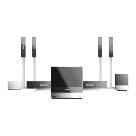
Page 10: Directions For Use
EN 10 3139 785 31510 Directions for use 3. Directions For Use DVD/ SACD Home Theater System HTS9800W Quick Start Guide Connect Set up Enjoy What’s in the box? DVD/ SACD HOME THEATER SYSTEM HTS9800W User Manual AV Wireless Receiver Box... - Page 11 3139 785 31510 EN 11 Directions For Use Connect Placement and Connections Connect the front speakers and subwoofer Assemble the speakers FRONT FRONT FRONT CENTER RIGHT LEFT Both the coloured stickers must SPEAKERS match CENTER RIGHT LEFT To AC power subwoofer Extend the FM pigtail antenna and...
- Page 12 Ensure the front of the AV Wireless Receiver Press SYSTEM MENU on the remote. box (with Philips logo) is facing towards the Press É to select { General Setup Page }. DVD system. Note If there is an interference on your...
-
Page 13: User Manual
DVD system panel. Need help? User Manual See the user manual that came with your Philips DVD/SACD Home Theater System. Online Go to www.philips.com/support. 2006 © Koninklijke Philips N.V. All rights reserved. - Page 14 EN 14 3139 785 31510 Dismantling Instructions Dismantling of the Main Unit 1) Remove Cover and loosen 7 screws as shown in 4) Loosen 2 screws to remove PSU Module. Figure 4-1. Figure 4-4 Figure 4-1 5) Loosen 4 screws to remove Bracket Pos 125. 2) Loose 4 screws to remove the Bracket Pos 131.
- Page 15 3139 785 31510 EN 15 7) Loosen 2 screws to remove the MPEG Board. Figure 4-7 Note: Please change from Ground Point A to Ground Point B to achieve Service Position for Display Board. Figure 4-8 Figure 4-9 Figure 4-10...
-
Page 16: Dismantling Instructions & Service Positions
EN 16 3139 785 31510 Dismantling Instructions & Service Positions Dismantling of Subwoofer Power Box 1) Remove the Base as shown in Figure 4-15. Subwoofer Figure 4-15 2) Loosen 5 screws as shown in Figure 2. Subwoofer Figure 4-16 3) Loosen 16 screws as shown in Figure 3 and pull the Power-Box Assy. - Page 17 3139 785 31510 EN 17 Dismantling Instructions & Service Positions Dismantling of the Junction Box 1) Loosen 2 screws. 2) Loosen 2 screws. Junction Box Europe Figure 4-22 Junction Box Figure 4-24 3) Loosen 4 screws. Junction Box Figure 4-25 Junction Box AP Figure 4-23...
- Page 18 EN 18 3139 785 31510 Dismantling Instructions & Service Positions Service Positions - Main Unit Service Position - PSU Unit Service Position - Display Board (Topview) Service Position - MPEG Board Service Position- Display Board (Bottomview) Service Position - Front Panel Board...
- Page 19 3139 785 31510 EN 19 Dismantling Instructions & Service Positions Service Positions - Junction Box, Subwoofer unit & Wireless Box Surround Service Position - Junction Box Service Position - Amplifier & Interface Board Service Position - PSU Module Service Position - Subwoofer...
-
Page 20: Service Test Program
EN 20 3139 785 31510 Service Test Program Service Test Program-Display Test To start service test program select AUX source. Press Select AUX source, press 2,5,8. (All 3 numbers must be keyed within 5 seconds). 2-5-8. All 3 numbers must be keyed in within 5 seconds. - Page 21 3139 785 31510 EN 21 Service Test Program 5.1.4 Procedure to upgrade the firmware 5.1.1 Reprogramming of DVD version Matrix 1. Power up the set and open tray. 2. Insert the prepared Upgrade CDROM and close the tray. After repair, the customer setting and region code may be lost. 3.
- Page 22 EN 22 3139 785 31510 Service Test Program Notes:...
-
Page 23: Block Diagram, Wiring Diagram
Block Diagram, Wiring Diagram 3139 785 31510 EN 23 Block Diagram U C D 74HC4052 M62429FP POWER AMP M62429FP U C D POWER AMP POWER AMP /RST RDS IC SAA6581T TUNER (TM 10) 3139_249_3297_Block_Diagram_Pg1.pdf_030806... - Page 24 Block Diagram, Wiring Diagram 3139 785 31510 EN 24 Block Diagram UCD AMP M62429FP Rs/Ls POWER AMP M62429FP UCD AMP Surr Cen POWER AMP 3139_249_3297_Block_Diagram_Pg2.pdf_030806...
-
Page 25: Wiring Diagram
Block Diagram, Wiring Diagram 3139 785 31510 EN 25 Wiring Diagram 1103 1401 1216-014-15S-AAF B3B-EH-A 1407 B12B-EH-A 1405 B6B-EH-A 1406 N10236-52B2VC 1400 1103 S2B-EH 1107 I2C_DAT I2C_Clk GND_D stby PWR_Fail +12Va TU_L A-GND TU_R 10FMN-SM1-A-TF 1105 Port Set Port Set S2B-EH 1108 Tuned... - Page 26 Block Diagram, Wiring Diagram 3139 785 31510 EN 26 Wiring Diagram RC_Out RC_Out GND_D GND_D RC_IN RC_IN GND_D GND_D FR_L FR_L GND_FR_L_R GND_FR_L_R MAINS FR_R FR_R To Interface Board SR_C SR_C Audio_L 9105 GND_SR_C GND_SR_C 3139 113 35571 FR_C A_Gnd FR_C GND_C_SUB GND_C_SUB...
-
Page 27: Circuit Diagram And Pwb Layout
Circuit Diagram and PWB Layout 3139 785 31510 EN 27 DVM 7.3 AV Board: Circuit Diagram (Part 1) 1101 D1 2204 H13 4137 A4 T154 I5 1102 G1 2205 H13 4138 A5 T155 E13 1104 I1 2206 H13 4139 A5 T156 E13 1105 I4 2207 H13... - Page 28 Circuit Diagram and PWB Layout 3139 785 31510 EN 28 DVM 7.3 AV Board: Circuit Diagram (Part 2) 1201 A11 T209 D7 2212 A11 T210 H10 T211 A11 2213 A11 2214 A11 T212 A11 2215 A11 T214 A11 3260 2216 A11 T215 A11 6200 6201...
- Page 29 Circuit Diagram and PWB Layout 3139 785 31510 EN 29 DVM 7.3 AV Board: Circuit Diagram (Part 3) 1301 B9 1302 D9 2301 A7 2302 E8 2303 E8 2304 D7 T301 2305 D7 T302 2306 E6 2307 C1 +HDMI_3V3_A 2308 B3 2309 C6 2310 C6 2311 D6...
- Page 30 Circuit Diagram and PWB Layout 3139 785 31510 EN 30 DVM 7.3 AV Board: Circuit Diagram (Part 4) 2401 A10 T409 C11 2402 A10 T410 D11 2403 A11 2404 A11 2405 C4 2407 D3 2408 D3 2409 D4 2410 D3 2411 D3 2413 E5 2414 E4...
- Page 31 Circuit Diagram and PWB Layout 3139 785 31510 EN 31 DVM 7.3 AV Board: Circuit Diagram (Part 5) 2501 C2 3569 F10 2502 B4 3570 F12 2504 E2 3571 F12 2505 E3 3572 F13 2506 F2 3573 G12 2507 E4 3574 G10 2508 B5 3575 G10...
- Page 32 Circuit Diagram and PWB Layout 3139 785 31510 EN 32 DVM 7.3 AV Board: Circuit Diagram (Part 6) 2612 A11 3688 I2 2613 A11 3689 I5 2615 C10 3690 A5 2616 C10 3691 E3 3612 3613 4605 2617 D9 3692 E3 680R 100R 2618 D11...
- Page 33 Circuit Diagram and PWB Layout 3139 785 31510 EN 33 DVM 7.3 AV Board: Circuit Diagram (Part 7) 1701 B12 1702 C12 1703 D12 1704 E12 1705 G12 1706 B12 2701 B7 2702 B7 2703 D7 2704 D7 2705 F7 2706 F7 2707 H7 2708 H7...
-
Page 34: Dvm 7.3 Av Board: Layout (Top View)
Circuit Diagram and PWB Layout 3139 785 31510 EN 34 DVM 7.3 AV Board: Layout (Top View) DVM73AV_Topview_31448.pdf_030806... -
Page 35: Dvm 7.3 Av Board: Layout (Bottom View)
Circuit Diagram and PWB Layout 3139 785 31510 EN 35 DVM 7.3 AV Board: Layout (Bottom View) DVM73AV_Bottomview_31448.pdf_030806... -
Page 36: Front Display: Schematic
Circuit Diagram and PWB Layout 3139 785 31510 EN 36 Front Display: Circuit Diagram (Part 1) 1101 A1 3183 B5 1102 C1 3184 B5 1103 F2 3185 B6 1104 D1 3186 B5 1105 B11 3187 B6 1107 A4 3188 B7 1107 1108 A4 3189 B6... - Page 37 Circuit Diagram and PWB Layout 3139 785 31510 EN 37 Front Display: Circuit Diagram (Part 2) 1201 B3 2201 D7 2202 E1 2203 E1 2204 E1 3201 B3 3202 B3 3203 C3 3204 B6 3205 B6 3206 C6 3207 D4 3208 E4 3209 D2 3210 D2...
-
Page 38: Front Display: Layout (Top View)
Circuit Diagram and PWB Layout 3139 785 31510 EN 38 Front Display: Layout (Top View) FrontDisplay_Topview_33206.pdf_030806... -
Page 39: Front Display: Layout (Bottom View)
Circuit Diagram and PWB Layout 3139 785 31510 EN 39 Front Display: Layout (Bottom View) FrontDisplay_Bottomview_33206.pdf_030806... -
Page 40: Front Led Panel: Schematic
Circuit Diagram and PWB Layout 3139 785 31510 EN 40 Front LED Panel: Circuit Diagram 1300 D1 1309 B5 2307 C1 2316 A8 2327 D7 3303 B1 3311 C2 3319 B4 3328 E4 3337 E9 3347 D8 3355 E4 3368 A2 3376 D6 3384 D9 3392 D4... -
Page 41: Front Led Panel: Layout (Top View)
Circuit Diagram and PWB Layout 3139 785 31510 EN 41 Front LED Panel: Layout (Top View) -
Page 42: Front Led Top: Schematic
Circuit Diagram and PWB Layout 3139 785 31510 EN 42 Front LED Top: Circuit Diagram Front LED Top: Layout (Top View) 1401 A1 3401 A2 6401 A2 F401 A1 F402 A1 1401 6401 F401 LTL-816TDK3 F402 3401 B2B-EH-A 3139_243_33175_a4_sh130_sh1.pdf_010606 Front LED Top: Layout (Bottom View) -
Page 43: Front Led Bottom: Schematic
Circuit Diagram and PWB Layout 3139 785 31510 EN 43 Front LED Bottom: Circuit Diagram Front LED Bottom: Layout (Top View) 1501 A1 3501 A2 6501 A2 1501 6501 LTL-816TDK3 3501 B2B-EH-A 3139_243_33185_a4_sh130_sh1.pdf_010606 Front LED Bottom: Layout (Bottom View) -
Page 44: Interface Board: Schematic
Circuit Diagram and PWB Layout 3139 785 31510 EN 44 Interface Board: Circuit Diagram (Part 1) 1101 A2 2106 F4 2118 B4 2131 E7 2142 D13 2153 D11 2164 B7 2177 A4 3111 B12 3122 B1 3135 E10 3146 G5 3161 C10 3176 A14 4109 A4... - Page 45 Circuit Diagram and PWB Layout 3139 785 31510 EN 45 Interface Board: Circuit Diagram (Part 2) 0201 B13 2201 D3 2214 A3 2225 A10 2235 F13 2249 F12 2258 H5 3209 F3 3219 A5 3229 C3 3238 C12 3248 D7 3257 C9 3266 D12 3275 F12...
-
Page 46: Interface Board: Layout (Top View)
Circuit Diagram and PWB Layout 3139 785 31510 EN 46 Interface Board: Layout (Top View) InterfaceBd_Topview_33156.pdf... -
Page 47: Interface Board: Layout (Bottom View)
Circuit Diagram and PWB Layout 3139 785 31510 EN 47 Interface Board: Layout (Bottom View) InterfaceBd_Bottomview_33156.pdf... -
Page 48: Mains Board: Schematic
Circuit Diagram and PWB Layout 3139 785 31510 EN 48 Mains Board: Circuit Diagram 1702 A10 1708 A4 1907 A4 2713 E10 2908 E4 2921 E4 3716 C9 3901 D6 3915 E4 5905 A1 6702 C3 6715 C9 6721 E10 6913 E5 7903 E7 9961 D9... -
Page 49: Mains Board: Layout
Circuit Diagram and PWB Layout 3139 785 31510 EN 49 Mains Board: Layout (Top View) PCB Main Board_Topview_33225.pdf_031606... -
Page 50: Wireless Interface Board: Schematic
Circuit Diagram and PWB Layout 3139 785 31510 EN 50 Wireless Interface Board: Circuit Diagram (Part 1) 1101 A1 6104 A7 1102 C1 6105 F4 1103 B6 7103 D3 1108 D1 7104 E2 2101 D1 7105 F4 1101 F101 2102 D2 7106 F2 F102 Surr_L... - Page 51 Circuit Diagram and PWB Layout 3139 785 31510 EN 51 Wireless Interface Board: Circuit Diagram (Part 2) 1201 E8 5209 C4 1202 E9 6200 C5 2200 A2 6201 C5 2201 B2 7111 A7 2202 A3 7112 B7 +12VA_Pre 2203 A3 7200-1 A4 3228 2204 A5...
- Page 52 Circuit Diagram and PWB Layout 3139 785 31510 EN 52 Wireless Interface Board: Circuit Diagram (Part 3) 1301 A8 F306 C8 1302 C8 1303 E8 2110 A3 2303 D7 2304 B4 2305 C2 +6V_ever 2306 E2 3342 GND_D LM393D 2307 F2 7302-1 2308 B7 470K...
-
Page 53: Wireless Interface Board: Layout (Top View)
Circuit Diagram and PWB Layout 3139 785 31510 EN 53 Wireless Interface Board: Layout (Top View) Wireless InterfaceBd_Topview_33506.pdf... -
Page 54: Wireless Interface Board: Layout (Bottom View)
Circuit Diagram and PWB Layout 3139 785 31510 EN 54 Wireless Interface Board: Layout (Bottom View) Wireless InterfaceBd_Bottomview_33506.pdf... -
Page 55: Pcba Soc: Schematic
Circuit Diagram and PWB Layout 3139 785 31510 EN 55 PCBA SOC: Circuit Diagram PCBA SOC: Layout (Top View) 1950 A2 1952 A3 5903 A2 5933 A2 9905 A2 T951 A2 1951 A1 1953 A3 5932 A2 9904 A2 T950 A2 5933 9904 1950... -
Page 56: Spk Panel: Schematic
Circuit Diagram and PWB Layout 3139 785 31510 EN 56 Spk Panel: Circuit Diagram 1500 A4 1503 B2 1506 D2 2502 B3 2509 D3 3501 A3 3504 B3 3507 C1 3510 D3 6501 B3 6504 C3 1501 A2 1504 B4 1507 B1 2505 C2 2510 D3... -
Page 57: Spk Panel: Layout (Top View)
Circuit Diagram and PWB Layout 3139 785 31510 EN 57 Spk Panel: Layout (Top View) Spk PanelBoard_Topview_33244.pdf... -
Page 58: Spk Panel: Layout (Bottom View)
Circuit Diagram and PWB Layout 3139 785 31510 EN 58 Spk Panel: Layout (Bottom View) Spk PanelBoard_Bottomview_33244.pdf... -
Page 59: Junction Box: Schematic
Circuit Diagram and PWB Layout 3139 785 31510 EN 59 Junction Box: Circuit Diagram 1400 D2 1403-1 D4 1405 C9 2405 A5 2408 B5 2411 D5 2414 E6 2417 E9 2420 E9 2423 A6 3403 D5 3406 D6 3409 A2 4405 E7 5400 B4 5403 E6... -
Page 60: Junction Box: Layout (Top View)
Circuit Diagram and PWB Layout 3139 785 31510 EN 60 Junction Box: Layout (Top View) Junction Board_Topview_35736.pdf... -
Page 61: Junction Box: Layout (Bottom View)
Circuit Diagram and PWB Layout 3139 785 31510 EN 61 Junction Box: Layout (Bottom View) Junction Board_Bottomview_35736.pdf... -
Page 62: Ucd Module Dev. Schematic
Circuit Diagram and PWB Layout 3139 785 31510 EN 62 UCD Module Dev: Circuit Diagram (Part1) 1100 C1 3182 F10 1105 E1 3183 C4 1110 C12 3184 I10 1115 D13 3185 I10 5100 1120 D13 3186 H4 2100 A2 3187 F10 2112 3128 2101 D1... - Page 63 Circuit Diagram and PWB Layout 3139 785 31510 EN 63 UCD Module Dev: Circuit Diagram (Part2) 1201 A1 2202 B1 2207 D8 2212 B1 3201 A4 3206 E6 3211 E7 3216 E4 3222 E2 3231 B3 3236 D9 4202 A2 6204 B9 7200 A5 7205 A9...
-
Page 64: Ucd Module Dev. Layout (Top View)
Circuit Diagram and PWB Layout 3139 785 31510 EN 64 UCD Module Dev: Layout (Top View) UCDModule _Topview_35364.pdf... -
Page 65: Ucd Module Dev. Layout (Bottom View)
Circuit Diagram and PWB Layout 3139 785 31510 EN 65 UCD Module Dev: Layout (Bottom View) UCDModule _Bottomview_35364.pdf... -
Page 66: Vga Conn Board Schematic & Layout
Circuit Diagram and PWB Layout 3139 785 31510 EN 66 VGA Conn Board: Circuit Diagram VGA Conn Board: Layout 1100 B4 1101 A1 1101 RC_out GND_D RC_in GND_D FR_L GND_FR_L/R FR_R 1100 SURR_C GND_SURR_C FRNT_C GND_C/SUB SURR_R GND_SURR_L/R SURR_L 15FMN-BTRK-A 16 17 1216-014-15S-AAF GND_D... -
Page 67: Psu - Main Unit And Wireless Box Surround
PSU - Main Unit and Wireless Box Surround 3139 785 31510 EN 67 PSU - Main Unit (For Information Only) 3122_427_24160_130_1_041109.pdf_110904... - Page 68 PSU - Main Unit and Wireless Box Surround 3139 785 31510 EN 68 PSU - Wireless Box Surround 3122_427_23995_130_132_pg1.pdf_081805...
-
Page 69: Psu - Wireless Box Surround
PSU - Main Unit and Wireless Box Surround 3139 785 31510 EN 69 PSU - Wireless Box Surround 3122_427_23995_130_132_pg2.pdf_081805... -
Page 70: Exploded View & Spare Parts List
Exploded View & Spare Parts List 3139 785 31510 EN 70 Exploded View of the Main Unit Set 3139_249_3429_Main Unit exploded view.pdf_091605... -
Page 71: Exploded View Of The Wireless Surround Box Set
Exploded View & Spare Parts List 3139 785 31510 EN 71 Exploded View of the Wireless Surround Box Set 3139_247_1213_Wireless Surround Box.pdf_091605... -
Page 72: Exploded View Of The Power Box Set
Exploded View & Spare Parts List 3139 785 31510 EN 72 Exploded View of the Power Box Set 3139_117_1079_Power Box.pdf_042304... - Page 73 3139 785 31510 EN 73 Exploded View & Spare Parts List Exploded View of the Speaker Box Speaker Box exploded View_03_16_06...
- Page 74 EN 74 3139 785 31510 Exploded View & Spare Parts List Exploded View of the Stands Stands exploded View_03_16_06...
-
Page 75: Spare Parts List
0141 3139 244 09641 CAB BTM JN BOX PNT HTS9800 0325 3139 247 12381 BOX SPK ASSY CS9800 0326 3139 247 12621 SUBWOOF TOTAL ASSY HTS9800W/37 0326 3139 247 12311 SUBWOOF TOTAL ASSY HTS9800W/12 0328 3139 247 12481 STANDS SPK HTS9800W... - Page 76 CAB TOP JN BOX PNT PRT HTS9800 0141 3139 244 09641 CAB BTM JN BOX PNT HTS9800 0326 3139 247 12391 SUBWOOF TOTAL ASSY HTS9800W/55 0328 3139 247 12481 STANDS SPK HTS9800W 0329 3139 247 12131 BOX WIRELESS SURR HTS9800...
Need help?
Do you have a question about the HTS9800W and is the answer not in the manual?
Questions and answers