Table of Contents
Advertisement
Quick Links
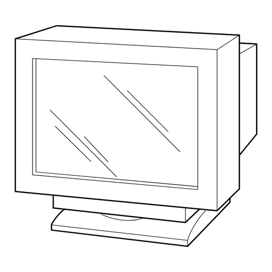
SERVICE MANUAL
CRT
Viewable image size
Maximum resolution
Standard image area
Deflection frequency*
AC input voltage/current
SPECIFICATIONS
0.24 mm aperture grille pitch
21 inches measured diagonally
90-degree deflection
FD Trinitron
Approx. 403.8 × 302.2 mm (w/h)
(16 × 12 inches)
19.8" viewing image
Horizontal: 1600 dots
Vertical: 1200 lines
Approx. 388 × 291 mm (w/h)
3
× 11
1
(15
/
/
inches)
8
2
or
Approx. 364 × 291 mm (w/h)
× 11
3
1
(14
/
/
inches)
8
2
Horizontal: 30 to 109 kHz
Vertical: 48 to 160 Hz
100 to 240 V, 50 – 60 Hz, 2.0 – 1.0 A
GDM-5403
Power consumption
Approx. 145 W
Approx. 498 × 491 × 478 mm (w/h/d)
Dimensions
(19
Mass
Approx. 32 kg (70 lb 9 oz)
Plug and Play
DDC1/2B/2Bi, GTF**
* Recommended horizontal and vertical timing condition
• Horizontal sync width duty should be more than 4.8% of total
horizontal time or 0.8 µs, whichever is larger.
• Horizontal blanking width should be more than 2.3 µsec.
• Vertical blanking width should be more than 450 µsec.
** If the input signal is Generalized Timing Formula (GTF)
compliant, the GTF feature of the monitor will automatically
provide an optimal image for the screen.
Design and specifications are subject to change without notice.
COLOR GRAPHIC DISPLAY
AEP Model
Chassis No. SCC-L22M-A
(OEM STD)
Chassis No. SCC-L22U-A
(ELSA, FORMAC)
G1
CHASSIS
× 19
× 18
5
3
7
/
/
/
inches)
8
8
8
Advertisement
Table of Contents

Related Manuals for Sony GDM-5403


Summary of Contents for Sony GDM-5403
-
Page 1: Service Manual
GDM-5403 SERVICE MANUAL AEP Model Chassis No. SCC-L22M-A (OEM STD) Chassis No. SCC-L22U-A (ELSA, FORMAC) CHASSIS SPECIFICATIONS 0.24 mm aperture grille pitch Power consumption Approx. 145 W Approx. 498 × 491 × 478 mm (w/h/d) 21 inches measured diagonally Dimensions ×... - Page 2 VIEWS AND IN THE PARTS LIST ARE CRITICAL FOR return the removed cover to the home position. SAFE OPERATION. REPLACE THESE COMPONENTS WITH SONY PARTS WHOSE PART NUMBERS AP- PEAR AS SHOWN IN THIS MANUAL OR IN SUPPLE- MENTS PUBLISHED BY SONY. CIRCUIT ADJUST-...
- Page 3 GDM-5403 POWER SAVING FUNCTION This monitor meets the power-saving guidelines set by VESA, * “Sleep” and “deep sleep” are power saving modes defined by the Environmental Protection Agency. NERGY TAR, and NUTEK. If the monitor is connected to a ** When your computer enters a power saving mode, the input signal is computer or video graphics board that is DPMS (Display Power cut and NO INPUT SIGNAL appears on the screen.
-
Page 4: Timing Specification
GDM-5403 TIMING SPECIFICATION MODE AT PRODUCTION MODE 1 MODE 2 RESOLUTION 1600 X 1200 1280 X 1024 CLOCK 229.500 MHz 157.500 MHz — HORIZONTAL — H-FREQ 106.250 kHz 91.146 kHz usec usec H. TOTAL 9.412 10.971 H. BLK 2.440 2.844 H. -
Page 5: Table Of Contents
GDM-5403 TABLE OF CONTENTS Section Title Page 1. GENERAL ..............1-1 2. DISASSEMBLY 2-1. Cabinet Removal ..........2-1 2-2. D Board Removal ..........2-1 2-3. G Board Removal ..........2-2 2-4. A Board Terminal Board Bracket Removal ............. 2-2 2-5. - Page 6 The operating instructions mentioned here are partial abstracts from the Operating Instruction Manual. The page numbers of the Operating Instruction Manual remain as in the manual. AC IN (HD15)
- Page 7 AC IN (HD15) AC IN (HD15)
-
Page 14: Disassembly
GDM-5403 SECTION 2 DISASSEMBLY 2-1. CABINET REMOVAL Push in the tip of a screwdriver about 5mm to unlock the claw. Cabinet Cabinet Two claws Four screws Bezel assembly Bezel assembly (+ BVTT 4 x 8) Cabinet Top cover Two screws... -
Page 15: G Board Removal
GDM-5403 2-3. G BOARD REMOVAL Four screws (+BVTP 3 x 8) G shield Three screws (+ BVTT 4 x 8) CN602 G board CN654 CN653 CN652 CN650 Two screws (+ BVTP 3 x 8) AC inlet (3P) Two hooks Open the G block in the direction of the arrow . -
Page 16: N Board Removal
GDM-5403 2-5. N BOARD REMOVAL CN5003 CN5002 CN001 CN5001 CN002 CN007 CN010 CN011 N board Printed circuit board holder 2-6. SERVICE POSITION CAUTION : SHORT D,G boards Rear shield If the claw is hooked, opening and closing the board is impossible. -
Page 17: Bezel Assembly, H Board Removal
GDM-5403 2-7. BEZEL ASSEMBLY, H BOARD REMOVAL Before removing the bezel assembly, secure the picture tube by attaching two screws to the picture tube shield at the positions shown with an arrow (diagonal two places) to prevent the picture tube from falling. (Use the screws +BVTT 4 x 8 that fix top cover.) -
Page 18: Picture Tube Removal
GDM-5403 2-9. PICTURE TUBE REMOVAL Remove the bezel assembly. (Refer to 2-7) Open the D block (Refer to 2-2.) A board Deflection yoke Anode cap Open the G block (Refer to 2-3.) Neck assembly Three connectors Picture tube • REMOVAL OF ANODE-CAP NOTE: Short circuit the anode of the picture tube and the anode cap to the metal chassis, CRT shield or carbon painted on the CRT, after removing the anode. -
Page 19: Harness Location
GDM-5403 2-10. HARNESS LOCATION J board H board Picture tube CN801 4pin 4pin CN651 CN601 CN650 CN603 CN5001 CN508 CN505 CN509 CN652 CN5003 CN502 CN5002 CN653 CN602 CN654 CN001 CN506 CN501 AC inlet G board D board N board Rear shield... -
Page 20: Safety Related Adjustment
GDM-5403 SECTION 3 SAFETY RELATED ADJUSTMENT When replacing or repairing the shown below table, the c) Beam Current Protector Circuit Check following operational checks must be performed as a (1st Protector): D Board safety precaution against X-rays emissions from the unit. -
Page 21: Adjustments
GDM-5403 SECTION 4 ADJUSTMENTS Note: Hand degauss must be used on stand-by or power-off condition. This model has an automatic earth magnetism correction function by using an earth magnetism sensor and a LCC coil. When using a hand degauss while monitor (LCC coil) is being operated, it sometimes gets magnetized, and the system may not work properly as a result. - Page 22 GDM-5403 Connect the communication cable of the computer to the connector located on the D board. Run the service software and then follow the instruction. 1-690-391-21 A-1500-819-A 3-702-691-01 Interface Unit Connector Attachment IBM AT Computer To BUS CONNECTOR as a Jig...
-
Page 23: Diagrams
SECTION 5 DIAGRAMS 5-1. BLOCK DIAGRAMS IC401 IC402 IC403 RGB DRIVE RGB DRIVE RGB AMP CN407 CN408 CN401 V901 ROUT ROUT ROUT HD15 PICTURE TUBE GOUT GOUT GOUT HEATER+ HEATER+ BOUT BOUT BOUT BIN1 INPUT GIN1 R DET IN RIN1 G DET IN IC406 B DET IN... - Page 24 µ-COM, V.CONV, H. CONV, LCC, GEO MAGNETIC SENSOR IC5301 (2/2) DET1 CN5002 LCC-LB (+) – STBY+5V LCC-LB LCC-LB (–) LCC-LT (+) IC5301 (1/2) LCC-LT IC001 LCC-LT (–) CPU/DSP LCC-RB (+) – IC011 LCC-RB LCC-RB (–) LCC-RT (+) IC5101 (2/2) LCC-RT LCC-RT (–) CN001 UPWM21...
- Page 25 (POWER SUPPLY) CN654 IC650 H CENT H +220V SHUNT REG S891 H CENT N POWER T620 CN891 TH601 CN603 H CENT L D650 AC L OUT AC L OUT +220V TO D BOARD AC L IN AC L IN +220V CN508 D610 (POWER SW)
-
Page 26: Frame Schematic Diagram
5-2. FRAME SCHEMATIC DIAGRAM CN401 INPUT1 HD15D-SUB VIDEO AMP, CN407 CN408 RGB OUT CN402 :S-MICRO PICTURE TUBE HEATER+ HEATER+ C BLOCK (CRT SOCKET) CONNECTOR PANEL GND CN010 CN504 :FFC +15V +15V +15V +15V -15V -15V -15V -15V STBY+5V STBY+5V HV DET HV DET CN507 CN654... -
Page 27: Circuit Boards Location
5-4. SCHEMATIC DIAGRAMS AND PRINTED 5-3. CIRCUIT BOARDS LOCATION Terminal name of semiconductors in silk screen Part Replaced ([) WIRING BOARDS printed circuit ( HV ADJ RV901 Note: Circuit Device Printed symbol Terminal name • All capacitors are in µF unless otherwise noted. (pF: µµF) Collector Capacitors without voltage indication are all 50 V. -
Page 28: Schematic Diagram Of A Board
(1) Schematic Diagram of A Board IC403 FA4301 5V-2 +12V IC401 C BLOCK IC402 RGB AMP M52757FP-TP M52749FP-TP R338 D101 RGB DRIVE RGB DRIVE R116 1PS226-115 C107 :CHIP 4.7k C101 C411 :CHIP R112 CN402 0.01 R_IN2 VCC2 OSD_BLK VCC2 R337 B:CHIP R105 (GND) - Page 29 • A BOARD IC401 M52757FP V901 PICTURE TUBE 21TKC Sync Sepa TO D BOARD T902(FBT)HV B-SS9272<AEP>-A..-P2-EPS05 • A BOARD IC402 M52749FP • A BOARD WAVEFORMS OSD IN (R) MAIN RETRACE INPUT (R) CLAMP OSD MIX OUTPUT (R) CONTRAST CONTRAST BLANKING VCC1 (R) CLAMP GND1 (R)
- Page 30 VIDEO AMP RGB OUT — A BOARD (Conductor Side) — • A BOARD — A BOARD (Component Side) — SEMICONDUCTOR LOCATION Conductor Component Side Side IC401 IC402 IC403 IC404 IC405 IC406 IC407 TRANSISTOR Conductor Component Side Side Q101 Q201 Q301 Q401 Q402 Q406...
-
Page 31: Schematic Diagrams Of H, J Boards
USER CONTROL POWER SW (2) Schematic Diagrams of H, J Boards Q803 DTA124ESA-TP 1W+5V LED DRIVE CN891 R813 S891 C810 POWER Q804 AC L OUT DTA124ESA-TP R823 Q801 LED DRIVE R824 2SC3311A STBY+5V CN801 AC L IN 1.5k LED DRIVE TO G BOARD WHT-L R811... -
Page 32: Schematic Diagram Of D Board
(3) Schematic Diagram of D Board TO A BOARD CN406 TO G BOARD CN654 CN506 CN508 :S-MICRO D922 ERA34-10TP1 R901 D901 100k 1SS133T-77 :CHIP R549 400V 0.47 R560 IC502 R574 C552 CN501 R553 C909 C910 R903 D908 1/2W 0.01 R917 LA6500-FA 100k C932... - Page 33 DEFLECTION • D BOARD WAVEFORMS — D BOARD — 8.8 Vp-p (H) 1.9 Vp-p (H) 568 Vp-p (H) 50.6 Vp-p (H) 54.5 Vp-p (H) 2.1 Vp-p (H) • D BOARD SEMICONDUCTOR LOCATION DIODE IC501 IC502 D504 IC503 D505 – IC701 D506 –...
-
Page 34: Schematic Diagrams Of N (A, B, C) Board
• Divided circuit diagram One sheet of N board circuit diagram is divided into three sheets, a b 1 each having the code N-a to N-c. For example, the destination Ref. No. (4) Schematic Diagrams of N (a, b, c) Board ab1 on the code N-a sheet is connected to ab1 on the N-b sheet. - Page 35 (µ-COM,GEO MAGNETIC SENSOR) STBY+5V IC006 TL082CPS-E20 ABL DET AMP GND10 AIN4 UPWM5 AVSS2 GND11 AIN3 MOIRECONT UPWM6 AIN2 KEYDET VDD9 AIN1 HSHPBAL TEMP UPWM7 AIN0 VDD10 AVDD1 UPWM8 DAC1 GND12 AVSS1 HDF0 GND13 DAC0 Q010 VCONV UPWM9 GND4 2SA1037AK INPUTSEL INV.
- Page 36 STBY+5V -15V +15V IC5401 IC5101 IC5301 IC5201 +15V LA6515 LA6515 LA6515 LA6515 V.S1 V.S1 V.S1 V.S1 OUT1 V.S2 OUT1 V.S2 OUT1 V.S2 OUT1 V.S2 OUT2 OUT2 OUT2 OUT2 -15V (H.V.CONV,LCC) B-SS9116<NH.>-N..-P3-EPS05 CN5001 CN5003 CN5002 :S-MICRO :S-MICRO :S-MICRO Schematic diagram Schematic diagram <...
- Page 37 µ-COM, V.CONV, H.CONV, LCC, GEO MAGNETIC SENSOR — N BOARD (Conductor Side) — • N BOARD — N BOARD (Component Side) — SEMICONDUCTOR LOCATION Conductor Component Side Side IC001 IC002 IC003 IC004 IC005 IC006 IC010 IC011 IC012 IC5101 IC5201 IC5301 IC5401 TRANSISTOR Conductor...
-
Page 38: Schematic Diagram Of G Board
(5) Schematic Diagram of G Board IC650 CN604 DM-57N (POWER SUPPLY) +220V SHUNT REG 5.7 2.5 CN654 R653 R652 R649 :S-MICRO 470k :CHIP :FPRD H CENT H C662 C661 R650 H CENT N 0.01 2200p 2.2k T620 :CHIP H CENT L D650 L650 +220V... - Page 39 POWER SUPPLY — G BOARD — • G BOARD SEMICONDUCTOR LOCATION IC610 IC630 IC650 IC651 IC652 IC653 IC654 IC680 TRANSISTOR Q603 – Q610 – Q621 – Q630 – Q631 – Q632 – Q633 Q650 – Q651 – Q652 Q653 Q654 Q667 Q670 Q671...
-
Page 40: Semiconductors
5-5. SEMICONDUCTORS M52749FP-TP DTA124ESA 2SC2362K-G ERA22-06AVRBT ON3171-R 1PS181-115 BA00AST-V5 BA9759F-E2 HA17431PA 2SJ360-TE12L DTA124ESA-TP 2SC2362KG-AA ERA22-08 BA05ST-V5 HA17431PA-TZ 2SA1175-HFE ERA34-10TP1 LA6500-FA 2SA1309A-QRSTA ERB38-06V1 2SC2459-GR-TPE4 GP08D 2SC2784 GP08DPKG23 2SC2785-HFE HSS83TD 2SC3311A-QRSTA P6KE200AG23 TOP VIEW TOP VIEW RD2.2M-T1B LETTER SIDE RGP02-20EL-6394 18pin SOP 42pin SOP CATHODE M52757FP-TP... -
Page 41: Exploded Views
GDM-5403 SECTION 6 EXPLODED VIEWS • Items with no part number and no • Items marked " * " are not stocked since The components identified 0 marked are description are not stocked because they they are seldom required for routine critical for safety. -
Page 42: Picture Tube
GDM-5403 6-2. PICTURE TUBE 7-685-663-71 +BVTP 4X16 7-685-881-09 +BVTT 4X8 The components identified 0 marked are critical for safety. Replace only with the part number specified. REF.NO. PART NO. DESCRIPTION REMARK REF.NO. PART NO. DESCRIPTION REMARK 0 1-419-128-21 COIL, DEGAUSSING... -
Page 43: Packing Materials
GDM-5403 6-3. PACKING MATERIALS The components identified 0 marked are critical for safety. Replace only with the part number specified. REF.NO. PART NO. DESCRIPTION REMARK REF.NO. PART NO. DESCRIPTION REMARK * 4-073-356-01 CUSHION (UPPER) (ASSY) 1-793-504-11 CABLE ASSY * 4-368-079-01 BAG, POLYETHYLENE... -
Page 44: Electrical Parts List
GDM-5403 ¡ The components identified marked are SECTION 7 critical for safety. Replace only with the part number specified. ELECTRICAL PARTS LIST The components identified by [ in this REF.NO. PART NO. DESCRIPTION REMARK REF.NO. PART NO. DESCRIPTION REMARK NOTE: •... - Page 45 GDM-5403 ¡ The components identified marked are critical for safety. Replace only with the part number specified. REF.NO. PART NO. DESCRIPTION REMARK REF.NO. PART NO. DESCRIPTION REMARK FB411 1-412-911-11 FERRITE 1.1µH C446 1-104-664-11 ELECT 47µF 20% 25V C449 1-109-982-11 CERAMIC CHIP 1µF...
- Page 46 GDM-5403 ¡ The components identified marked are critical for safety. Replace only with the part number specified. REF.NO. PART NO. DESCRIPTION REMARK REF.NO. PART NO. DESCRIPTION REMARK R137 1-249-413-11 CARBON 1/4W R406 1-216-097-91 RES-CHIP 100K 1/10W R138 1-216-017-91 RES-CHIP 1/10W...
- Page 47 GDM-5403 ¡ The components identified marked are critical for safety. (a)(g) Replace only with the part number specified. REF.NO. PART NO. DESCRIPTION REMARK REF.NO. PART NO. DESCRIPTION REMARK SG401 1-576-354-21 GAP, SPARK C657 1-104-664-11 ELECT 47µF 20% 25V SG402 1-519-422-11 GAP, SPARK...
- Page 48 GDM-5403 ¡ The components identified marked are critical for safety. Replace only with the part number specified. REF.NO. PART NO. DESCRIPTION REMARK REF.NO. PART NO. DESCRIPTION REMARK D681 8-719-109-89 ZENER DIODE RD5.6ESB2 Q652 8-729-120-28 TRANSISTOR 2SC1623-L5L6 D682 8-719-121-26 ZENER DIODE RD9.1ESL2...
- Page 49 GDM-5403 ¡ The components identified marked are critical for safety. (g)(d) Replace only with the part number specified. REF.NO. PART NO. DESCRIPTION REMARK REF.NO. PART NO. DESCRIPTION REMARK R659 1-216-049-91 RES-CHIP 1/10W <VARISTOR> R660 1-216-073-00 RES-CHIP 1/10W VDR601 ¡ 1-801-268-51 VARISTOR TNR14V471K660...
- Page 50 GDM-5403 ¡ The components identified marked are critical for safety. Replace only with the part number specified. REF.NO. PART NO. DESCRIPTION REMARK REF.NO. PART NO. DESCRIPTION REMARK C535 1-163-021-91 CERAMIC CHIP 0.01µF 10% 50V C905 1-163-127-00 CERAMIC CHIP 270pF C536 1-126-967-11 ELECT 47µF...
- Page 51 GDM-5403 ¡ The components identified marked are critical for safety. Replace only with the part number specified. REF.NO. PART NO. DESCRIPTION REMARK REF.NO. PART NO. DESCRIPTION REMARK D519 8-719-988-61 DIODE 1SS355TE-17 JR006 1-216-295-91 SHORT D520 8-719-988-61 DIODE 1SS355TE-17 JR008 1-216-295-91 SHORT...
- Page 52 GDM-5403 ¡ The components identified marked are critical for safety. Replace only with the part number specified. REF.NO. PART NO. DESCRIPTION REMARK REF.NO. PART NO. DESCRIPTION REMARK Q903 8-729-901-87 TRANSISTOR 2SC2411K-CQ R547 1-219-726-11 METAL Q904 8-729-901-97 TRANSISTOR 2SA1036K-Q R548 1-249-437-11 CARBON...
- Page 53 The components identified by in this GDM-5403 ¡ The components identified marked are manual have been carefully factory- selected for eachset in order to satisfy critical for safety. regulations regarding X-ray radiation. Replace only with the part number specified. Should replacement be required, replace only with the value originally used.
- Page 54 GDM-5403 ¡ The components identified marked are critical for safety. (h)(j)(n) Replace only with the part number specified. REF.NO. PART NO. DESCRIPTION REMARK REF.NO. PART NO. DESCRIPTION REMARK * A-1372-740-AH BOARD, COMPLETE [ELSA, FORMAC] <THERMISTOR> * A-1646-207-AH BOARD, COMPLETE [OEM STD]...
- Page 55 GDM-5403 ¡ The components identified marked are critical for safety. Replace only with the part number specified. REF.NO. PART NO. DESCRIPTION REMARK REF.NO. PART NO. DESCRIPTION REMARK C033 1-163-021-91 CERAMIC CHIP 0.01µF 10% 50V C097 1-126-964-11 ELECT 10µF 20% 50V C098 1-163-021-91 CERAMIC CHIP 0.01µF...
- Page 56 GDM-5403 ¡ The components identified marked are critical for safety. Replace only with the part number specified. REF.NO. PART NO. DESCRIPTION REMARK REF.NO. PART NO. DESCRIPTION REMARK D002 8-719-062-51 DIODE 1PS226-115 D003 8-719-062-51 DIODE 1PS226-115 IC006 8-759-700-78 IC NJM082M D004...
- Page 57 GDM-5403 ¡ The components identified marked are critical for safety. Replace only with the part number specified. REF.NO. PART NO. DESCRIPTION REMARK REF.NO. PART NO. DESCRIPTION REMARK R030 1-216-049-91 RES-CHIP 1/10W R1003 1-216-049-91 RES-CHIP 1/10W R031 1-216-669-11 METAL CHIP 5.6K 0.5% 1/10W...
- Page 58 GDM-5403 ¡ The components identified marked are critical for safety. Replace only with the part number specified. REF.NO. PART NO. DESCRIPTION REMARK REF.NO. PART NO. DESCRIPTION REMARK R1062 1-216-049-91 RES-CHIP 1/10W R5510 1-249-382-11 CARBON 1/4W F R1063 1-216-065-91 RES-CHIP 4.7K...
- Page 59 GDM-5403 Sony Corporation English Computer Display Company 2000AL05052-1 9-978-668-01 Computer Display DIV. Printed in Japan 2000. 1 – 78 –...
Need help?
Do you have a question about the GDM-5403 and is the answer not in the manual?
Questions and answers