
Related Manuals for Motorola PRO3150


Summary of Contents for Motorola PRO3150
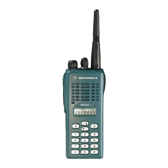
- Page 1 PRO3150 ™ Portable Radio c o n t a c t PRO3150 c o n t ro l Detailed Service Manual...
-
Page 2: Computer Software Copyrights
Accordingly, any copyrighted Motorola computer programs contained in the Motorola products described in this manual may not be copied or reproduced in any manner without the express written permission of Motorola. Furthermore, the purchase of Motorola products shall not be... -
Page 3: Safety Information
SAFE AND EFFICIENT OPERATION OF MOTOROLA TWO-WAY RADIOS This document provides information and instructions for the safe and efficient operation of Motorola Portable and Mobile Two-Way Radios. The information provided in this document supersedes the general safety information contained in user guides published prior to January 1, 1998. -
Page 4: Electromagnetic Interference/Compatibility
ELECTROMAGNETIC INTERFERENCE/COMPATIBILITY NOTE Nearly every electronic device is susceptible to electromagnetic interference (EMI) if inadequately shielded, designed, or alternately configured for electromagnetic compatibility. To avoid electromagnetic interference and/or compatibility conflicts, turn off your radio in any facility where posted notices instruct you to do so. Hospital or health facilities may be using equipment that is sensitive to external RF energy. -
Page 5: Introduction
In instances where the product is covered under a “return for replacement” or “return for repair” warranty, a check of the product should be performed prior to shipping the unit back to Motorola. This is to ensure that the product has been correctly programmed or has not been subjected to damage outside the terms of the warranty. -
Page 6: Technical Support
Aftermarket Division (AAD). If no part number is assigned, the part is not normally available from Motorola. If the part number is appended with an asterisk, the part is serviceable by Motorola Depot only. If a parts list is not included, this generally means that no user-serviceable parts are available for that kit or assembly. - Page 7 Radio Model Information Table 1-1 Radio Model Number (Example: LAH34KDC9AA1AN) Type of Model Freq. Power Physical Channel Feature Model Model Protocol Unit Series Band Level Packages Spacing Level Revision Package 4-5W Prog- Conventional (136-174 Display ramma- MHz) UHF R1 1-Line (403-470 Display MHz)
- Page 8 Radio Model Information Notes __________________________________________________________________________ __________________________________________________________________________ __________________________________________________________________________ __________________________________________________________________________ __________________________________________________________________________ __________________________________________________________________________ __________________________________________________________________________ __________________________________________________________________________ __________________________________________________________________________ __________________________________________________________________________ __________________________________________________________________________ __________________________________________________________________________ __________________________________________________________________________ __________________________________________________________________________ __________________________________________________________________________ __________________________________________________________________________ __________________________________________________________________________ __________________________________________________________________________ __________________________________________________________________________ __________________________________________________________________________ __________________________________________________________________________ __________________________________________________________________________ __________________________________________________________________________ __________________________________________________________________________ __________________________________________________________________________ __________________________________________________________________________ __________________________________________________________________________ __________________________________________________________________________ __________________________________________________________________________ __________________________________________________________________________ __________________________________________________________________________ __________________________________________________________________________ __________________________________________________________________________ __________________________________________________________________________ __________________________________________________________________________...
-
Page 9: Table Of Contents
TABLE OF CONTENTS Safe And Efficient Operation Of Motorola Two-way Radios ......iii Exposure To Radio Frequency Energy.............iii Portable Radio Operation And EME Exposure ..........iii Electromagnetic Interference/Compatibility ............iv Operational Warnings ..................iv Operational Cautions ..................iv Introduction 1.1 Scope of Manual....................1-1 1.2 Warranty and Service Support................1-1 1.2.1 Warranty Period ..................... - Page 10 2.9.1 Power Amplifier ....................2-12 2.9.2 Antenna Switch ....................2-12 2.9.3 Harmonic Filter .....................2-13 2.9.4 Antenna Matching Network ................2-13 2.9.5 Power Control Integrated Circuit (PCIC) ............2-13 2.10 VHF Receiver.....................2-14 2.10.1 Receiver Front-End ..................2-14 2.10.2 Receiver Back-End..................2-15 2.10.3 Automatic Gain Control (AGC) ..............2-15 2.10.4 Frequency Generation Circuitry..............2-16 2.11 Synthesizer ......................2-16 2.12 Voltage Control Oscillator (VCO) ...............2-17...
-
Page 11: Theory Of Operation
Introduction Chapter 2 Theory of Operation Introduction This chapter provides a detailed theory of operation for the radio components. Schematic diagrams for the circuits described in the following paragraphs are located in Chapter 4 of this manual. Radio Power Distribution A block diagram of the DC power distribution throughout the radio board is shown in Figure 2-1. - Page 12 Radio Power Distribution Accessory Jacks Keypad/Option Board Audio PA Vdda UNSWB+ Vdda Reg. Fuse SWB+ 7.5V Vddd Vdda Battery Reg. FRACTN ASFIC_CMP LVZIF MCU Micro P, ROM Driver VCOBIC & EEPROM Control MECH. SWB+ On/Off Switch Reg. Low Battery Detect Ant.
-
Page 13: Keypad
Keypad Keypad The keypad block diagram is shown in Figure 2-2. The comparator compares the voltage when any one of the keypad row or keypad column keys is pressed. Pressing a key sends a message to the microprocessor through the output (KEY_INT) line signifying that a key has been pressed. The microprocessor then samples the Analog to Digital voltages at the keypad row and keypad column, and makes a comparison with a map table to identify the key pressed. -
Page 14: Controller
Controller Controller The controller board is the central interface between the various subsystems of the radio. It is separated into MCU digital and audio/signalling functions as shown in Figure 2-3. To Synthesizer Internal/ External 16.8 MHz Microphone Reference Clock Audio/Signalling from Synthesizer Architecture External... -
Page 15: Uhf Transmitter
UHF Transmitter UHF Transmitter The UHF transmitter consists of the following basic circuits as shown in Figure 2-4. • Power amplifier (PA) • Antenna switch/harmonic filter • Antenna matching network • Power control integrated circuit (PCIC) PCIC Antenna Vcontrol Vcontrol Jack Antenna Switch/ From VCO... -
Page 16: Harmonic Filter
UHF Transmitter 2.5.3 Harmonic Filter The harmonic filter consists of C104, L102, C143, C103, L101, C142 and C102. The harmonic filter for UHF is a modified Zolotarev design optimized for efficiency of the power module. This type of filter has the advantage that it can give a greater attenuation in the stop-band for a given ripple level. The harmonic filter insertion loss is typically less than 1.2dB. -
Page 17: Uhf Receiver
UHF Receiver UHF Receiver The UHF receiver consists of front end, back end, and automatic gain control circuits. A block diagram of the receiver is shown in Figure 2-5. Detailed descriptions of these stages are contained in the paragraphs that follow. Antenna Pin Diode Varactor... -
Page 18: Receiver Back-End
UHF Receiver The output of the post-RF amplifier filter is connected to the passive double balanced mixer consisting of components T301, T302, and CR306. Matching of the filter to the mixer is provided by C381. After mixing with the first local oscillator (LO) signal from the voltage controlled oscillator (VCO) using low side injection, the RF signal is down-converted to a 45.1 MHz IF signal. -
Page 19: Frequency Generation Circuit
Synthesizer circuit, as RSSI generated by U301 is lower at cold temperatures compared to normal operation at room temperature. Resistor R300 and capacitor C397 form an R-C network used to dampen any transient instability while the AGC is turning on. 2.6.4 Frequency Generation Circuit The frequency generation circuit, shown in Figure2-6, is composed of Fractional-N synthesizer U201 and VCO/Buffer IC U241. - Page 20 2-10 Voltage Controlled Oscillator (VCO) To achieve fast locking for the synthesizer, an internal adapt charge pump provides higher current at pin 45 of U201 to put the synthesizer within the lock range. The required frequency is then locked by normal mode charge pump at U201, pin 43.
- Page 21 Voltage Controlled Oscillator (VCO) 2-11 The operation logic is shown in Table 2-2. AUX3 (U201 Pin2) Level Shifter AUX4 (U201 Pin3) Network U201 Pin 32 Prescaler Out TRB_IN Pin 20 Pin 19 Pin 12 Pin7 Rx-SW Tx/Rx/BS Pin13 Tx-SW Switching Network LO RF INJECTION Presc Vcc-Superfilter...
-
Page 22: Antenna Switch
2-12 VHF Transmitter U241-10 is injected into the input of the PA module (U101-16). Also in transmit mode, the audio signal to be frequency modulated onto the carrier is received through U201-41. When a high impedance is applied to U241-19, the VCO operates in battery saver mode. In this mode, both the receive and transmit oscillators, as well as the receive transmit and prescaler buffer, are turned off. -
Page 23: Antenna Matching Network
VHF Transmitter 2-13 the shunt diode to a high impedance at the input of the harmonic filter. In the receive mode, the diodes are both off, creating a low attenuation path between the antenna and receiver ports. 2.9.3 Harmonic Filter The harmonic filter consists of C3532 to C3536, L3531 and L3532. -
Page 24: Receiver Front-End
2-14 VHF Receiver 2.10 VHF Receiver The VHF receiver consists of front end, back end, and automatic gain control circuits. A block diagram of the VHF receiver is shown in Figure 2-10. Detailed descriptions of these features are contained in the paragraphs that follow. -
Page 25: Automatic Gain Control (Agc)
VHF Receiver 2-15 The output of the post-RF amplifier filter is connected to the passive double balanced mixer which consists of T3301, T3302 and CR3301. Matching of the filter to the mixer is provided by C3317, C3318 and L3308. After mixing with the first LO signal from the voltage controlled oscillator (VCO) using high side injection, the RF signal is down-converted to the 45.1 MHz IF signal. -
Page 26: Frequency Generation Circuitry
2-16 Synthesizer current gain NPN transistor, is drawn through the PIN diode to turn it on. Maximum current flowing through the pin is limited by resistors R3316, R3313, R3306 and R3324. Feedback capacitor C3326 is used to provide some stability to this high gain stage. An additional gain control circuit is formed by Q3201 and associated components. -
Page 27: Voltage Control Oscillator (Vco)
Voltage Control Oscillator (VCO) 2-17 In achieving fast locking for the synthesizer, an internal adapt charge pump provides higher current at pin 45 of U3701 to put the synthesizer within lock range. The required frequency is then locked by normal mode charge pump at pin 43. Both the normal and adapt charge pumps get their supply from the capacitive voltage multiplier made up of C3701 to C3704 and triple diodes D3701and D3702. - Page 28 2-18 Voltage Control Oscillator (VCO) at the VCO. This voltage is a DC voltage typically between 3.5V and 9.5V when the PLL is locked on frequency. AUX3 (U3701 Pin2) U3701 Pin 32 Prescaler Out TRB_IN Pin 20 Pin 19 Pin 12 Pin7 Rx-SW TX/RX/BS...
- Page 29 Voltage Control Oscillator (VCO) 2-19 During the transmit condition, when PTT is depressed, 3.2 volts is applied to U3801, pin 19. This activates the transmit VCO by enabling the transmit oscillator and the transmit buffer of U3801. The RF signal at U3801, pin 10 is injected into the input of the PA module (U3501, pin16). This RF signal is the TX RF INJECTION.
- Page 30 2-20 Voltage Control Oscillator (VCO)
-
Page 31: Maintenance
Introduction Chapter 3 Maintenance Introduction This section of the manual describes: • preventive maintenance • safe handling of CMOS devices • repair procedures and techniques Preventive Maintenance The radios do not require a scheduled preventive maintenance program; however, periodic visual inspection and cleaning is recommended. -
Page 32: Safe Handling Of Cmos And Ldmos
When damaged parts are replaced, identical parts should be used. If the identical replacement component is not locally available, check the parts list for the proper Motorola part number and order the component from the nearest Motorola Communications parts center listed in the “Piece Parts”... - Page 33 General Repair Procedures and Techniques To remove a chip component: • Use a hot-air hand piece and position the nozzle of the hand piece approximately 1/8" (0.3 cm) above the component to be removed. • Begin applying the hot air. Once the solder reflows, remove the component using a pair of tweezers.
-
Page 34: Recommended Test Tools
Recommended Test Tools Recommended Test Tools Table 3-1 lists the tools recommended for working on this family of radios. These tools are also available from Motorola Table 3-1 Recommended Test Tools Motorola Part Description Application Number RSX4043 Torx Driver Tighten and remove chassis screws... -
Page 35: Replacing The Circuit Board Fuse
Replacing the Circuit Board Fuse Table 3-1 Recommended Test Tools Motorola Part Description Application Number 6680334B49 0.410” x 0.410” Heat-focus heads for R-1319A work station 6680334B50 0.430” x 0.430” 6680334B51 0.492” x 0.492” 6680334B52 0.572” x 0.572” 6680334B53 0.670” x 0.790”... -
Page 36: Removing And Reinstalling The Circuit Board
2. Lift the circuit board out of the radio chassis, then remove and discard the thermal pad located between the circuit board and chassis. 3. After repairs, replace the thermal pad (Motorola P/N 7580556Z01) then reinstall the circuit board into the radio chassis. -
Page 37: Power Up Self-Test Error Codes
“EPM ERR” Codeplug structure Reprogram codeplug with correct version and retest mismatch, non radio. If message reoccurs, replace main board or existence of code- send radio to nearest Motorola Depot. plug. “EPM CS” Codeplug check- Reprogram codeplug. sum is wrong. -
Page 38: Uhf Troubleshooting Charts
UHF Troubleshooting Charts UHF Troubleshooting Charts Troubleshooting Flow Chart for Controller MCU Check Press PTT. Red LED does not Before replacing light up Power Up Not able to pro- MCU, check SPI Alert Tone gram RF Board AUDIO Audio at clock, SPI data, J402 Audio AudioPA... - Page 39 UHF Troubleshooting Charts Troubleshooting Flow Chart for Receiver (Sheet 1 of 2) START Bad SINAD Bad 20dB Quieting No Recovered Audio Audio at pin Check Controller 27 of U301? Spray of inject 1st IF into XTAL Filter IF Freq: 45.1MHz Check Q320 bias circuitry for faults.
- Page 40 3-10 UHF Troubleshooting Charts Troubleshooting Flow Chart for Receiver (Sheet 2 of 2) Inject RF into J101 Trace IF signal Q302 collec- from L311 to IF Signal at tor OK? Q302. Check for L311? IF signal bad XTAL filter. present? Before replacing U301, check U301 voltages;...
- Page 41 UHF Troubleshooting Charts 3-11 Troubleshooting Flow Chart for Transmitter START No Power Is There B+ Bias for Check Q111 Ant switch CR101 Is Control Voltage Check PCIC Is Current High or Low at C119 High Check Drive to Module 1. Check Pin Diodes 2.
-
Page 42: Troubleshooting Flow Chart For Synthesizer
3-12 UHF Troubleshooting Charts Troubleshooting Flow Chart for Synthesizer Check U248, 3.3V at U201 Start L201 & L202 pins 5, 20, 34 & Visual Check CR201, U210, Correct check of the U211, C258, C259 & Problem Board OK? C228 Is U201 Pin 47 Is 16.8MHz 16.8MHz at pin 6 of... - Page 43 UHF Troubleshooting Charts 3-13 Troubleshooting Flow Chart for VCO START Change U241 No LO? Change L253 O/C? L253 U241 TRB = Pin 10 5V? @U241 Tx Carrier? >1V? Pin 19 VCO OK Check R245 for dry joint or faulty AUX 3 Check High? R260...
-
Page 44: Vhf Troubleshooting Charts
3-14 VHF Troubleshooting Charts 3.10 VHF Troubleshooting Charts Troubleshooting Flow Chart for Controller MCU Check Press PTT. Red LED does not Before replacing light up Power Up Not able to pro- MCU, check SPI Alert Tone gram RF Board AUDIO Audio at clock, SPI data, J402 Audio... - Page 45 VHF Troubleshooting Charts 3-15 Troubleshooting Flow Chart for Receiver (Sheet 1 of 2) START Bad SINAD Bad 20dB Quieting No Recovered Audio Audio at pin Check Controller 27 of U3220? Spray of inject 1st IF into XTAL Filter IF Freq: 45.1MHz Check Q3270 bias circuitry for faults.
- Page 46 3-16 VHF Troubleshooting Charts Troubleshooting Flow Chart for Receiver (Sheet 2 of 2) Inject RF into J3501 Trace IF signal Q3200 collec- from C3200 to IF Signal at tor OK? Q3200. Check for C3200? IF signal bad XTAL filter. present? Before replacing U3220, check U3220 volt-...
- Page 47 VHF Troubleshooting Charts 3-17 START No Power Is There B+ Bias for Check Ant switch Q3561 D3521 Control Voltage High or Is Current Check PCIC Low at TP3502 High Check Drive to Module 1. Check Pin Diodes 2. Check Harmonic Filter Is Drive Troubleshoot Inspect/Repair Tx.
- Page 48 3-18 VHF Troubleshooting Charts Troubleshooting Flow Chart for Synthesizer Check U3201, 3.3V at U3701 Start L3731 pins 5, 20, 34 & Visual Check D3701, Correct check of the D3702, U3701, C3701 Problem Board OK? - C3707 Is 16.8MHz 16.8MHz Replace at pin 6 of Is U3701 Pin 47 Signal at...
- Page 49 VHF Troubleshooting Charts 3-19 Troubleshooting Flow Chart for VCO START Change U3801 L3831, Change L3832, No LO? L3831, L3832 L3833 O/C? U3801 TRB = 3.2V? Tx Carrier? Pin 10 >1V? VCO OK Check R3811, L3811 for dry joint AUX 3 at or faulty Check U3701...
-
Page 50: Keypad Troubleshooting Chart
3-20 Keypad Troubleshooting Chart 3.11 Keypad Troubleshooting Chart Troubleshooting Flow Chart for Keypad START Tone Disconnect and Generated reconnect 9-pin flex Disconnect and Keypad reconnect 40-pin flex... -
Page 51: Schematic Diagrams, Overlays, And Parts Lists
1. Unless otherwise stated, resistances are in Ohms (k = 1000), and capacitances are in picofarads (pF) or microfarads (µF). 2. DC voltages are measured from point indicated to chassis ground using a Motorola DC multime- ter or equivalent. Transmitter measurements should be made with a 1.2 µH choke in series with the voltage probe to prevent circuit loading. -
Page 52: Six Layer Circuit Board
Flex Layout 4.1.2 Six Layer Circuit Board SIDE 1 LAYER 1 (L1) LAYER 2 (L2) LAYER 3 (L3) INNER LAYERS LAYER 4 (L4) LAYER 5 (L5) LAYER 6 (L6) SIDE 2 Figure 4-1. Six-Layer Circuit Board: Copper Steps in Layer Sequence Flex Layout Front Metal <- TO KP... -
Page 53: Keypad-Controller Interconnect Flex Schematic
Keypad-Controller Interconnect Flex Schematic Keypad-Controller Interconnect Flex Schematic CONTROLLER KEYPAD J601 J400 FLAT_RX_SND FLAT_RX_SND RX_AUD_RTN RX_AUD_RTN TX_AUD_SND TX_AUD_SND TX_AUD_RTN TX_AUD_RTN FLAT_TX_RTN FLAT_TX_RTN OPT_ENA OPT_ENA URX_SND URX_SND MISO MISO KEYPAD_ROW KEYPAD_ROW KEYPAD_COL KEYPAD_COL SWB+ SWB+ SWB+ SWB+ KEY_INT KEY_INT LEDBL LEDBL Vddd Vddd Vddd... -
Page 54: Keypad Top And Bottom Overlays
Keypad-Controller Interconnect Flex Schematic 4.3.1 Keypad Top and Bottom Overlays M605 M604 M606 M622 M623 M608 M610 M611 M612 TP16 TP15 M613 M614 M615 TP14 M616 M617 M618 M619 M620 M621 Figure 4-4. Keypad-Top Overlay J600 R627 R636 C610 C609 C611 R618 C612... -
Page 55: Speaker Microphone Schematic
INT_MIC 100pF INT_SPN M400 SPKR_20 SPKR_20 ZMY0130346-O Figure 4-6. Speaker Microphone Schematic 4.4.1 Speaker Microphone Assembly Table 4-1 Speaker Microphone Assembly Parts List Reference Motorola Part No. Description Designator C800 2113740A55 Capacitor, 100pF M400 5085738Z02 Speaker M401 5013920A04 Microphone, Mini... - Page 56 Speaker Microphone Schematic This page intentionally left blank...
- Page 57 Chapter 4 J601 44-Pin Connector J601-44 J601-43 J601-42 J601-41 J601-40 FLAT_RX_SND J601-39 J601-38 RX_AUD_RTN J601-37 J601-36 TX_AUD_SND J601-35 TX_AUD_RTN J601-34 J601-33 FLAT_TX_RTN J601-32 OPT_ENA J601-31 J601-30 J601-29 URX_SND J601-28 J601-27 MISO J601-26 J600 11-Pin Connector J601-25 KEYPAD_ROW J601-24 KEYPAD_COL J601-23 J601-22 SWB+ J600-1...
- Page 58 Table 4-1 Keypad Board Parts List Reference Motorola Part Description Designator C603 2113740F51 100pF C606 2113743E20 0.1uF C607 2113740F51 100pF C609 2113740F51 100pF C610 2113740F51 100pF C611 2113740F51 100pF C612 2113928D08 10uF C613 2113740F51 100pF C614 2113740F51 100pF C615 2113740F51...
- Page 59 Chapter 4 INT_SPN INT_MIC UNSWB+ C475 J402 10uF J402-1 C489 1000pF J402-2 INT_MIC R473 J402-3 INT_SPN J402-4 C442 0.1uF U420 R423 C471 C472 TDA8547 100pF 100pF C470 100pF C447 R472 Speaker/Mic Connector 0.1uF 3.6K IN1POS OUT1POS IN1NEG OUT1NEG C486 C488 1000pF 1000pF IN2POS...
- Page 60 4-10 4V_3.3V RSSI BATT_CODE R462 100K 3.28V Q419-2 R498 Q431-1 R405 R402 100K R499 R493 R494 SWB+ Vddd Q400 TP406 BATT_PULL_UP UNSWB+ C401 C400 R401 0.1uF .01uF FLAT_SW R406 R427 C443 U400 C402 0.1uF 7.45V LP2951ACMM-3.3 0.1uF C403 R461 CR412 10uF INPUT OUTPUT...
- Page 61 4-11 Vddd F1200 Vddd R457 Q418 TP401 1.90V TEST_POINT 3.28V R418 4.7K C493 FLAT_SW UNSWB+ Vddd Vddd Vddd R437 C431 C449 C453 C423 100pF 100pF 100pF 100pF L411 390nH U410 L410 ILC7062CM-33 3.3V 390nH R411 C456 VOUT 3 100pF C434 EE_CS 0.1uF C435...
- Page 62 4-12 FLASH ROM Figure 4-11. Controller Memory Schematic Diagram...
- Page 63 4-13 INT_SPN INT_MIC UNSWB+ C475 J402 10uF J402-1 C489 1000pF J402-2 INT_MIC R473 J402-3 INT_SPN J402-4 C442 0.1uF U420 R423 C471 C472 TDA8547 100pF 100pF C470 100pF C447 R472 Speaker/Mic Connector 0.1uF IN1POS OUT1POS 3.6K IN1NEG OUT1NEG AUDIO C486 C488 1000pF 1000pF IN2POS...
- Page 64 4-14 C466 C458 100pF 100pF C459 100pF R481 J400 40-Pin Connector J400-1 FLAT_RX_SND J400-2 J400-3 RX_AUD_RTN J400-4 C467 J400-5 0.1uF J400-6 TX_AUD_SND TX_AUD_RTN J400-7 C482 C481 J400-8 0.1uF 0.1uF FLAT_TX_RTN J400-9 J400-10 OPT_ENA J400-11 J400-12 J400-13 URX_SND J400-14 J400-15 MISO C463 J400-16 100pF...
- Page 65 4-15 R410 PB504 PB502 PB501 R437 SH323 R300 R352 VR440 C397 FL201 RT301 R314 R321 C527 VR501 C328 C363 C325 R335 C362 U405 TP201 U406 R338 L325 C528 J400 R325 C385 C351 C353 SH201 C384 C352 Q505 U247 R355 Q316 C220 L311 C349...
- Page 66 4-16 VR441 VR506 SH402 C522 C489 C345 C278 L330 C359 C338 S502 C330 C277 C358 C357 C326 R350 R463 C344 C390 CR501 R344 CR414 C383 C327 C360 R311 R415 U301 C346 B501 C361 R312 R414 U409 C343 C329 C494 C336 SH202 C433 C208...
- Page 67 4-17 PB501 SWITCH UNSWB+ VR451 J407 VR450 F501 C521 10.0V VR440 10.0V B501 .01uF 6.8V SWITCH MECH_SWB+ S502 C503 C500 PB504 TAB2 RSSI_FIL C502 CR501 100pF 1000pF SWITCH L505 0.47uF 390nH TAB1 BATT_CODE VR439 VR444 6.8V VR506 6.8V R507 PB502 SWITCH INT_SPN C508...
- Page 68 4-18 DACRx C322 82pF R342 -65.5dBm@45.1MHz 100K L310 150nH R308 R305 C314 C315 R310 100pF 0.1uF R304 C380 R309 .01uF L304 -63.4dBm@403.355MHz CR306 C321 180nH -60.5dBm@469.985MHz 100pF C306 T301 XFMR C309 -54.4dBm@403.355MHz C308 100pF -51.8dBm@469.985MHz R306 R307 100pF 100K 100K C312 C310 C316...
- Page 69 4-19 L331 R343 2.2uH Vdd_FILTERED Vdda C382 (SOURCE) 10uF DEMOD R350 C348 C347 C344 C346 C345 100K 0.1uF 0.1uF 0.1uF 0.1uF 0.1uF C390 C329 100pF 0.1uF C343 0.22uF R344 R355 SH323 SH321 SH322 SHIELD SHIELD SHIELD Q320 2.628V 3.185V C383 R345 C384 C342...
- Page 70 4-20 U210 U211 TC7SET04FU TC7SET04FU C265 C257 C296 100pF 0.1uF C256 100pF C258 7.697V .01uF U247 ADP3300 C259 SWB+ C299 .01uF 100pF (SOURCE) CR201 C291 C294 C293 0.47uF L202 4V_3.3V U248 100pF 0.47uF 2.2uH LP2980 L203 C277 C278 2.2uH C230 C229 C228 100pF...
- Page 71 4-21 C281 R245 100pF R242 L243 C250 RESONATOR 7.5pF C276 C285 C286 2.2uF 100pF 4.567V (Rx) 0.1uF 4.613V (Tx) C246 100pF L281 L273 R241 390nH 33nH C242 7.5pF C272 C273 0.1uF C243 L271 L242 R244 7.5pF 68nH 220nH C245 RX_INJ 2.4pF TX_INJ TX_OUT...
- Page 72 4-22 E101 BEAD R102 UNSWB+ L107 C114 C123 33.47nH 100pF 10uF C172 UNSWB+ 0.1uF R106 C109 L106 100pF 7.66nH Microstrip Microstrip R172 L108 L109 C121 C160 L112 TX_OUT 11.03nH 100pF 100pF 390nH Q110 4.22nH Microstrip C118 100pF C130 C111 C112 C113 C128 100pF...
- Page 73 4-23 ANT_BIAS C108 L105 100pF 390nH C142 C143 RF_JACK 2.7pF J101 C101 RF_JACK L101 L102 100pF CR101 15.22nH 15.22nH TX_OUT C104 C102 C103 5.6pF 6.8pF C141 L104 L116 3.3pF 15.22nH 9.75nH RX_IN CR102 ANTENNA_CONTACT C107 J104 C106 3.9pF C140 R170 C144 43pF SH100...
- Page 74 4-24 Table 4-2: UHF Band 1Radio Parts List Circuit Motorola Circuit Motorola Circuit Motorola Description Description Description Circuit Motorola Part No. Part No. Part No. Description Part No. C172 2113740F51 100pF C276 2104993J02 2.2uF C340 2180478Z20 1.0uF C173 2113743M08 0.022uF...
- Page 75 4-25 Circuit Motorola Circuit Motorola Circuit Motorola Circuit Motorola Description Description Description Description Part No. Part No. Part No. Part No. C420 2113743L41 0.01uF C486 2113743L17 1000pF CR440 4813833C02 DUAL DIODE COMMON L307 2479990C01 13.9nH C421 2113928N01 0.1uF C487 Not Placed...
- Page 76 2680554Z01 RX PRE FILTER SHIELD 7580671Z01 PAD (FLEXIBLE CIRCUIT) R303 0662057M89 4.3K R423 0662057N39 470K SH302 2680555Z01 RX POST FILTER/RX AMP * Motorola Depot Servicing only R304 0662057N01 R425 0662057N10 SH303 2680509Z01 SHIELD, MIXER R305 0662057M67 R427 0662057M98 SH304 2680624Z01...
- Page 77 4-27 R410 PB501 PB504 PB502 R437 SH323 R300 R352 VR440 FL201 C397 RT301 R314 R321 C527 C363 VR501 C328 R335 C325 C362 U405 TP201 R338 L325 C528 J400 R325 C385 C351 C353 SH201 C352 C384 Q505 U247 C349 R355 C220 L311 Q316 Q320...
- Page 78 4-28 VR441 SH402 C489 C278 C359 L330 C338 S502 C277 C358 C357 R350 C344 C390 CR501 CR414 C383 R344 C360 R415 R311 C346 C361 R414 R312 C343 C494 SH202 C433 C431 C208 C263 Q418 L261 CR203 C204 R460 C223 L314 C264 R204 C219...
- Page 79 4-29 PB501 SWITCH UNSWB+ VR451 VR450 J407 F501 C521 10.0V VR440 10.0V B501 .01uF 6.8V SWITCH S502 MECH_SWB+ PB504 C503 C500 TAB2 RSSI_FIL C502 CR501 1000pF SWITCH 100pF L505 0.47uF 390nH TAB1 BATT_CODE VR439 VR444 6.8V VR506 6.8V R507 PB502 SWITCH INT_SPN C509...
- Page 80 4-30 DACRx C322 82pF R342 -63.8dBm@45.1MHz 100K L310 150nH R308 C315 R310 R305 C314 0.1uF 100pF R304 C380 R309 .01uF L304 -51.7dBm@450.125MHz CR306 C321 180nH C306 -52.6dBm@526.925MHz 100pF T301 XFMR C309 C308 100pF R306 R307 100pF 100K C312 100K C310 C316 C318 L305...
- Page 81 4-31 L331 R343 2.2uH Vdd_FILTERED Vdda C382 (SOURCE) 10uF DEMOD R350 C348 C347 C344 C346 C345 100K 0.1uF 0.1uF 0.1uF 0.1uF 0.1uF C390 C329 100pF 0.1uF C343 0.22uF R344 R355 SH323 SH321 SH322 SHIELD SHIELD SHIELD Q320 2.628V 3.185V C383 R345 C384 C342...
- Page 82 4-32 U210 U211 TC7SET04FU TC7SET04FU C265 C257 C296 100pF 0.1uF C256 100pF C258 7.5V .01uF 1.65V U247 ADP3300 C259 SWB+ C299 .01uF 100pF (SOURCE) CR201 C291 C294 C293 10uF L202 4V_3.3V 100pF 0.47uF U248 2.2uH LP2980 L203 C277 C278 2.2uH C230 C229 C228...
- Page 83 4-33 C281 R245 100pF R242 L243 C250 C276 C285 RESONATOR 4.3pF C286 2.2uF 100pF 4.6V 0.1uF C246 L281 L273 100pF R241 390nH 18nH C242 4.3pF C272 C273 1.1pF 0.1uF C243 L271 L242 R244 4.3pF 27nH 22nH C245 RX_INJ 2.7pF TX_INJ TX_OUT TX_IADJ CR243...
- Page 84 4-34 E101 BEAD R102 UNSWB+ L107 C114 C123 33.47nH 100pF 10uF C172 UNSWB+ 0.1uF R106 C109 L106 100pF 7.66nH Microstrip Microstrip R172 TX_OUT L108 L109 C121 C160 L112 4.22nH 11.03nH 100pF 100pF 390nH Q110 Microstrip C118 100pF C130 C111 C112 C113 C128 100pF...
- Page 85 4-35 ANT_BIAS C108 L105 100pF 390nH C142 C143 RF_JACK 2.7pF J101 C101 RF_JACK L102 L101 100pF CR101 11.81nH 11.81nH TX_OUT C104 C102 C103 5.1pF 6.8pF L104 L116 C141 11.81nH 16.28nH 8.2pF RX_IN CR102 ANTENNA_CONTACT C107 J104 C106 3.9pF C140 R170 C144 43pF SH100...
- Page 86 4-36 Table 4-3 UHF Band 2 Radio Parts List Circuit Motorola Circuit Motorola Circuit Motorola Description Description Description Circuit Motorola Part No. Part No. Part No. Description Part No. C171 2113743N50 100pF C264 2113743N50 100pF C331 2113743N50 100pF C172 2113740F51...
- Page 87 4-37 Circuit Motorola Circuit Motorola Circuit Motorola Circuit Motorola Description Description Description Description Part No. Part No. Part No. Part No. C410 2113928N01 0.1uF C477 2113743N50 100pF CR251 4862824C01 Varactor L242 2462587V26 22nH C411 2113743M24 0.1uF C478 2113743N50 100pF CR252...
- Page 88 4-38 Circuit Motorola Circuit Motorola Circuit Motorola Circuit Motorola Description Description Description Description Part No. Part No. Part No. Part No. Q421 4880214G02 R305 0662057M66 R427 0662057M98 SH304 2680624Z01 Shield, Mixer Diode Q431 5180159R01 Dual NPN R306 0662057N23 100K R428...
- Page 89 4-39 C517 C531 C529 R410 PB504 PB502 PB501 R437 C3205 R3200 R3217 C3212 C3213 VR440 R3209 Y3761 C3270 R3202 Y3200 C3279 C3210 R3275 VR501 R3226 C3278 C3277 C527 R3225 U405 TP3702 R3212 C528 C3214 C3203 Q3270 R3274 R3201 J400 TP3701 L3200 R3213 R3204...
- Page 90 4 - 40 VR441 VR506 SH402 C489 C3240 C3223 C3219 C3241 R3219 C3227 D3761 C3763 R3224 R3222 C3236 S502 C3243 Y3762 C3237 R3223 R3760 R463 C3244 R3761 U3220 CR501 CR414 C3230 C3235 C3751 C3221 R415 R3763 B501 R414 U409 C3735 C494 SH3702 C433...
- Page 91 4-41 PB501 SWITCH UNSWB+ VR450 VR451 J407 F501 C521 10.0V VR440 10.0V B501 .01uF 6.8V SWITCH MECH_SWB+ S502 C503 C500 PB504 TAB2 RSSI_FIL C502 CR501 100pF 1000pF SWITCH L505 0.47uF 390nH TAB1 BATT_CODE VR439 VR444 6.8V VR506 6.8V R507 PB502 SWITCH INT_SPN C509...
- Page 92 4 - 42 R5_2_FE R5_3_FE C3320 C3337 C3309 R3316 82pF .022uF 0.1uF L3309 150nH R3322 UNSWB_PLUS_1_RX UNSWB_PLUS_2_RX R3321 R3323 UNSWB+ IF_1_FE C3308 L3304 330pF 470nH C3336 10uF C3307 C3315 R3315 100pF 10pF T3301 C3317 R3310 39pF C3313 C3316 150pF 3.3pF C3318 C3311 C3312...
- Page 93 4-43 Vdd_FILTERED Vdd_FILTERED C3208 R5_3_ZIF R3209 0.1uF R3220 R3200 4.7K R3206 Q3201 RSSI C3220 100K C3204 R3201 C3205 10pF .01uF 2.2K 0.1uF L3221 R3207 R3208 R3212 4.7K 2.9V C3228 R3221 Y3200 .01uF C3229 C3210 1000pF C3225 XTAL R3202 100pF C3239 0.1uF 4.7K L3202...
- Page 94 4 - 44 U3711 7.5V ADP3300 5V_1_FN SWB_PLUS_1_FN 5V (SOURCE) SWB+ C3711 10uF C3712 C3713 0.1uF C3701 L3701 2.2uF 390nH .01uF R3701 C3702 .01uF D3701 C3710 C3703 2.2uF .01uF C3704 .01uF BIAS_ADJ 13.2V BIAS_ADJ_1_FN R3702 R3705 D3702 C3705 0.1uF C3714 4.7uF C3725 C3708...
- Page 95 4-45 Vdda VSF_1_VCO Vdda_3_VCO 3.3V 4.55V R5_1_VCO L3813 R:4V R3817 T: 2.8V R3802 R3811 R:4.6V R, T: 3.5V-9.5V T: 0V @ 135MHz-174MHz C3822 C3813 R: 1V RMS 1000pF R3818 R: 250mV RMS D3821 C3810 L3811 L3812 C3811 C3812 .01uF C3830 C3825 VCTRL_1_VCO C3804...
- Page 96 4 - 46 RESET UNSWB+ UNSWB+ UNSWB+ UNSWB+ DATA RESET_1_PA 5V_2_PA BIAS_TUNING CLK_2_PA C3570 330pF R3570 DATA_2_PA R3569 Q3561 CSX_2_PA C3560 UNSWB_LPLUS_2_PA UNSW_LPLUS_3_PA GND2 BPOS DATA R3561 U3502 H99S-4 TEMP C3566 RSET LM50C 100pF F168 5185963A15 R3571 C3561 ANT_BIAS R3562 R3563 .022uF C3565...
- Page 97 Table 4-4: VHF Radio Parts List Circuit Motorola Circuit Motorola Circuit Motorola Description Description Description Circuit Motorola Part No. Part No. Part No. Description Part No. C3301 2113743N29 13pF C3525 2113740F35 10pF C3731 2113743L41 .01uF C3302 2113743N54 150pF C3526 2113743M08 .022uF...
- Page 98 Circuit Motorola Circuit Motorola Circuit Motorola Circuit Motorola Description Description Description Description Part No. Part No. Part No. Part No. C409 2113743M24 0.1uF, +80%/-20% C485 2113743L17 1000pF E400 2480640Z01 Ferrite Bead L3824 2462587N68 C410 2113928N01 0.1uF, 10% C486 2113743L17 1000pF...
- Page 99 R403 Not Placed RT400 0680590Z01 Thermistor 33K 7580671Z01 pad (flexible circuit) R3546 0662057N11 R405 0662057M01 S501 4080502B03 Channel Switch * Motorola Depot Servicing only R3547 0662057N01 R406 0662057N20 S502 1880619Z01 Volume Switch R3548 0662057M95 7.5K R410 0662057N23 100K SH3201 2602023X08...
- Page 100 This page intentionally left blank...
- Page 102 , Motorola, Professional Radio, PRO Series, PRO3150, are trademaks of Motorola. LTR is a registered tademark of E.F. Johnson, Inc. SmarTrunk is a registered trademark of SmarTrunk Systems, Inc. Transcrypt is a registered tademark of Transcrypt International.
Need help?
Do you have a question about the PRO3150 and is the answer not in the manual?
Questions and answers