Advertisement
SERVICE MANUAL
Ver 1.0 1999. 03
Dolby noise reduction manufactured under license
from Dolby Laboratories Licensing Corporation.
"DOLBY" and the double-D symbol a are trade-
marks of Dolby Laboratories Licensing Corporation.
MICROFILM
WM-FX673/FX877
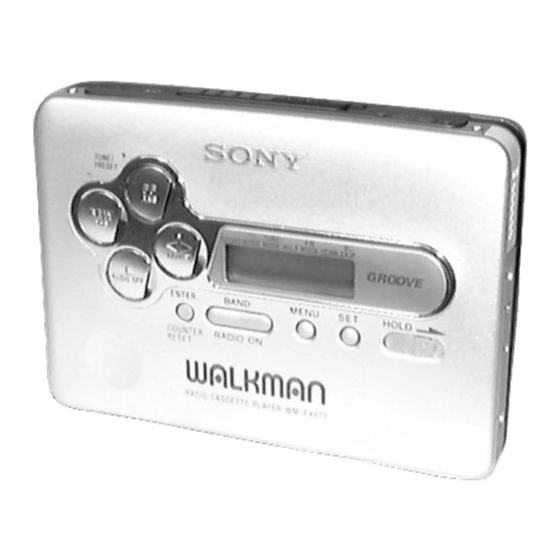
Photo: WM-FX673
SPECIFICATIONS
Canadian Model
Australian Model
Model Name Using Similar Mechanism
Tape Transport Mechanism Type
RADIO CASSETTE PLAYER
AEP Model
UK Model
WM-FX673
E Model
WM-FX673/FX877
Chinese Model
Tourist Model
WM-FX877
WM-EX670/EX672
MT-WMEX672-162
Advertisement
Table of Contents

Subscribe to Our Youtube Channel
Related Manuals for Sony WM-FX673


Summary of Contents for Sony WM-FX673
- Page 1 Australian Model WM-FX673 E Model WM-FX673/FX877 Chinese Model Tourist Model WM-FX877 Photo: WM-FX673 Dolby noise reduction manufactured under license Model Name Using Similar Mechanism WM-EX670/EX672 from Dolby Laboratories Licensing Corporation. Tape Transport Mechanism Type MT-WMEX672-162 “DOLBY” and the double-D symbol a are trade- marks of Dolby Laboratories Licensing Corporation.
-
Page 2: Table Of Contents
SUR LES DIAGRAMMES SCHÉMATIQUES ET LA LISTE DES PIÈCES SONT CRITIQUES POUR LA SÉCURITÉ DE FONCTIONNEMENT. NE REMPLACER CES COM- POSANTS QUE PAR DES PIÈCES SONY DONT LES NUMÉROS SONT DONNÉS DANS CE MANUEL OU DANS LES SUPPLÉMENTS PUBLIÉS PAR SONY. -
Page 3: Servicing Notes
SECTION 1 SERVICING NOTES This set detects the rotation of the idler gear (A) (side S) using the 3. FF, REW modes PH1 (photo reflector). The PH1 is mounted on the MAIN board, (1) Check that the preset state is set. therefore the idler gear (A) (side S) cannot be detected with the (2) Input the square wave or sine wave to the Q15-1 (COLLEC- MAIN board removed. - Page 4 Slider (NR) Rotation system Rotation system during PLAY. gear (NR) (FWD : left side/ REV : right side) idler gear (A) (side S) idler gear (A) (side T) gear (REEL) (side S) gear (REEL) (side T) motor pulley slider (NR) cam gear clutch assy (F) gear (Y)
-
Page 5: General
SECTION 2 This section is extracted from instruction manual. GENERAL (FX673) (FX877) (FX673) (FX877) – 5 –... - Page 6 (FX877) (FX673) (FX877) (FX673) (FX673) (FX877) – 6 –...
-
Page 7: Disassembly
SECTION 3 DISASSEMBLY This set can be disassembled in the order shown below. Case Block Assy Main Board Belt (F2) Motor (Capstan/Reel) (M601) Ornament Lid Block Pinch Lever Block Assy, Holder (F) Assy Assy, Head, Magnetic (HP901) (N)/(R) Assy Reel Cassette Note: Follow the disassembly procedure in the numerical order given. - Page 8 MAIN BOARD 2 Remove four solders of leaf switch. 3 Remove two solders of plunger solenoid. 5 two screws 6 MAIN board 5 screw (M1.4) 4 Remove four solders of motor. 1 flexible board Note: On installation MAIN board adjust the S1 and slider. slider BELT (F2) 2 terminal board (T3)
- Page 9 MOTOR (CAPSTAN/REEL) (M601) 1 two screws (M1.4) 2 motor (capstan/reel) (M601) LID BLOCK ASSY, CASSETTE 1 screw (M1.4 × 2) 5 lid block assy, cassette 2 two screws (M1.4 × 2) 3 Open the cassette lid. 4 shaft – 9 –...
- Page 10 ORNAMENT BLOCK ASSY, REEL 4 claw 5 ormanent block assy, reel 4 claw 3 boss 1 claw 1 claw 2 claw HOLDER (F) ASSY 2 shaft 7 bracket (cassette) assy 5 lever (S), lock 3 lever (B), lock 1 two screws (M1.4 ×...
- Page 11 PINCH LEVER (N)/(R) ASSY 1 claw 2 Remove the pinch lever (R) assy in the dereciton of the arrow. 4 Remove the pinch lever (N) assy in the direction of the arrow. 3 claw HEAD, MAGNETIC (PLAY BACK) (HP901) 1 claw 2 Remove the magnetic head (HP901) in the direction of the arrow.
-
Page 12: Mechanical Adjustments
SECTION 4 SECTION 5 MECHANICAL ADJUSTMENTS ELECTRICAL ADJUSTMENTS PRECAUTION PRECAUTION 1. Clean the following parts with a denatured-alcohol-moistened 1. Specified voltage : 1.3 V (DC) swab: 2. Setting playback head pinch roller BL SKIP : OFF rubber belts capstan SOUND RV/MB/GRV : OFF 2. - Page 13 0 dB=1 µV AM IF ADJUSTMENT TUNER SECTION Adjust for a maximum reading on level meter [AM] 450 kHz Setting: function : RADIO AM VCO VOLTAGE ADJUSTMENT BAND button : AM Adjustment Part Frequency Display Reading on Digital Voltmeter Put the lead-wire 531 kHz 1.5 ±...
-
Page 14: Diagrams
WM-FX673/FX877 SECTION 6 6-2. BLOCK DIAGRAM – MAIN Section – DIAGRAMS B+ SWITCH DDC B+ 6-1. BLOCK DIAGRAM – TUNER Section – Q304 10.7MHz TUNER L-CH FM/AM IF AMP,FM/AM DET, MPX (Page 16) (Page 15) IC2 (1/2) FM RF AMP, MIX AMP, OSC... -
Page 16: Schematic Diagram
WM-FX673/FX877 6-4. SCHEMATIC DIAGRAM • • See page 27 for Waveform. See page 28 for IC Block Diagrams. – 23 – – 24 – – 25 – – 26 –... -
Page 17: Ic Pin Function Description
• Waveform • IC Block Diagrams 6-5. IC PIN FUNCTION DESCRIPTION – MAIN BOARD – • MAIN BOARD IC3 TC9327AF-606 (SYSTEM CONTROLLER, LIQUID CRYSTAL DISPLAY DRIVER) IC1 TA7371AF-EL IC2 TA2022AFN-EL IC302 NJM2185AV-TE2 1 IC3 &¢ (X OUT) Pin No. Pin Name Description 500 mV/DIV, 5 µs/DIV 1 to 4... - Page 18 Pin No. Pin Name Description BOOST CTL Bass boost control signal output to the TA2123AF (IC301) “L”: off, “H”: on Emphasizing sound control signal output to the TA2123AF (IC301) REVIVE CTL “L”: RV (revive), “H”: normal/MB (mega bass)/GRV (groove) Emphasizing sound control signal output to the TA2123AF (IC301) MB/GRV CTL “L”: normal/RV (revive)/GRV (groove), “H”: MB (mega bass) Power on/off control signal output to the TA2123AF (IC301)
-
Page 19: Exploded Views
SECTION 7 EXPLODED VIEWS NOTE: • Abbreviation • -XX and -X mean standardized parts, so they • Items marked “*” are not stocked since they may have some difference from the original are seldom required for routine service. Some AUS : Australian model one. - Page 20 (2) MECHANISM DECK SECTION (MT-WMEX672-162) M601 PM901 HP901 Ref. No. Part No. Description Remark Ref. No. Part No. Description Remark X-3376-293-1 HOLDER (F) ASSY (FX877) 3-029-287-01 SPRING (TG), TORSION X-3377-039-1 HOLDER (F) ASSY (/M) (FX673) 3-029-268-01 FLYWHEEL (R), INSERT (FX877) X-3377-363-1 PINCH LEVER (R) ASSY 3-029-268-11 FLYWHEEL (R), INSERT (FX673) 3-029-271-01 SPRING (HD)
-
Page 21: Electrical Parts List
SECTION 8 MAIN ELECTRICAL PARTS LIST NOTE: • Due to standardization, replacements in the • Items marked “*” are not stocked since they The components identified by mark ! or dotted line with mark are seldom required for routine service. parts list may be different from the parts speci- ! are critical for safety. - Page 22 MAIN Ref. No. Part No. Description Remark Ref. No. Part No. Description Remark C206 1-115-156-11 CERAMIC CHIP C207 1-113-619-11 CERAMIC CHIP 0.47uF 6.3V 8-719-422-37 DIODE MA8051-TX D101 8-719-422-37 DIODE MA8051-TX C208 1-115-467-11 CERAMIC CHIP 0.22uF D201 8-719-422-37 DIODE MA8051-TX C210 1-164-677-11 CERAMIC CHIP 0.033uF D301...
- Page 23 MAIN Ref. No. Part No. Description Remark Ref. No. Part No. Description Remark 1-216-833-11 RES,CHIP 1/16W L803 1-412-010-41 INDUCTOR CHIP 22uH 1-216-853-11 METAL CHIP 470K 1/16W < LIQUID CRYSTAL DISPLAY > 1-216-821-11 METAL CHIP 1/16W 1-216-849-11 METAL CHIP 220K 1/16W 1-803-469-11 DISPLAY PANEL, LIQUID CRYSTAL 1-216-829-11 METAL CHIP 4.7K...
- Page 24 MAIN Ref. No. Part No. Description Remark Ref. No. Part No. Description Remark 1-218-831-11 RES,CHIP 0.5% 1/16W R803 1-216-817-11 METAL CHIP 1/16W 1-218-875-11 RES,CHIP 0.5% 1/16W R804 1-216-805-11 METAL CHIP 1/16W 1-218-839-11 RES,CHIP 0.5% 1/16W R805 1-216-819-11 METAL CHIP 1/16W 1-218-875-11 RES,CHIP 0.5% 1/16W...
- Page 25 WM-FX673/FX877 Ref. No. Part No. Description Remark Ref. No. Part No. Description Remark 1-528-543-11 BATTERY, NICKEL CADMIUM (NC-6WM) (FX673: E, EA, HK, AUS/FX877: CH) 1-528-543-22 BATTERY, NICKEL CADMIUM (NC-6WM) (FX673: AEP, UK. E, FR, EE, EA, HK, AUS/ FX877) 1-528-580-21 BATTERY CHARGER (BC-7HT) (FX877: JE)
Need help?
Do you have a question about the WM-FX673 and is the answer not in the manual?
Questions and answers