Table of Contents
Advertisement
CX-JDS22/JDS33
SERVICE MANUAL
Ver. 1.0 2006.02
CX-JDS22/JDS33 are the Amplifier, CD player, Tape
Deck and Tuner section in DBX-DS22/DS33.
Amplifier section
JDS33
The following measured at AC 120, 127, 220, 230,
240 V 50/60 Hz
DIN power output (rated): 120 + 120 watts (6 ohms at
1 kHz, DIN)
Continuous RMS power output (reference):
150 + 150 watts (6 ohms at
1 kHz, 10% THD)
JDS22
The following measured at AC 120, 127, 220, 230,
240 V 50/60 Hz
DIN power output (rated): 96 + 96 watts (6 ohms at
1 kHz, DIN)
Continuous RMS power output (reference):
120 + 120 watts (6 ohms at
1 kHz, 10% THD)
Inputs
AUDIO IN (stereo mini jack):
voltage 250 mV,
impedance 47 kilohms
MIC (phone jack) (except for European model):
sensitivity 1 mV,
impedance 10 kilohms
Outputs
PHONES (stereo mini jack):
accepts headphones of
8 ohms or more
SPEAKER:
accepts impedance of 6 to
16 ohms
Sony Corporation
9-887-087-01
Personal Audio Division
2006B1678-1
Published by Sony Techno Create Corporation
© 2006.02
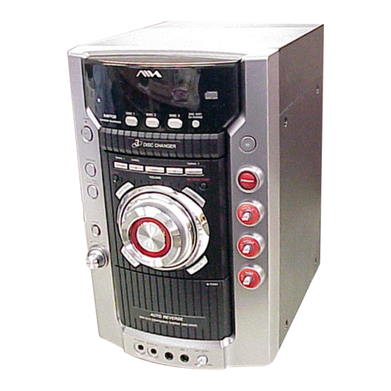
Photo : CX-JDS33
Model Name Using Similar Mechanism
CD
CD Mechanism Type
Section
Optical Pick-up Name
Model Name Using Similar Mechanism
TAPE
Section
Tape Transport Mechanism Type
SPECIFICATIONS
CD player section
System
Compact disc and digital
audio system
Laser Diode Properties
Emission duration:
continuous
Laser Output: Less than
44.6 µW
(This output is the value
measurement at a distance
of 200 mm from the
objective lens surface on
the Optical Pick-up Block
with 7 mm aperture)
Frequency response
2 Hz – 20 kHz (±0.5 dB)
Signal-to-noise ratio
More than 90 dB
Dynamic range
More than 90 dB
Tape deck section
Recording system
4-track 2-channel, stereo
Frequency response
50 – 13,000 Hz (±3 dB),
using Sony TYPE I
cassettes
Tuner section
FM stereo, FM/AM superheterodyne tuner
COMPACT DISC DECK RECEIVER
E Model
CX-JDS30
BU-F1BD81AA
KSM-215DCP/C2NP
CX-JDS20/JDS30
JDS22
CMAL5Z220A
JDS33
CMAL1Z240A
FM tuner section
Tuning range
87.5 – 108.0 MHz
(50 kHz step)
Antenna
FM lead antenna
Antenna terminals
75 ohms unbalanced
Intermediate frequency
10.7 MHz
AM tuner section
Tuning range
Pan-American models:
530 – 1,710 kHz
(with the tuning interval
set at 10 kHz)
531 – 1,710 kHz
(with the tuning interval
set at 9 kHz)
Other models:
530 – 1,710 kHz
(with the tuning interval
set at 10 kHz)
531 – 1,602 kHz
(with the tuning interval
set at 9 kHz)
Antenna
AM loop antenna
Antenna terminals
External antenna terminal
Intermediate frequency
450 kHz
— Continued on next page —
Advertisement
Table of Contents

Related Manuals for Aiwa CX-JDS22


Summary of Contents for Aiwa CX-JDS22
- Page 1 CX-JDS22/JDS33 SERVICE MANUAL E Model Ver. 1.0 2006.02 CX-JDS22/JDS33 are the Amplifier, CD player, Tape Deck and Tuner section in DBX-DS22/DS33. Photo : CX-JDS33 Model Name Using Similar Mechanism CX-JDS30 CD Mechanism Type BU-F1BD81AA Section Optical Pick-up Name KSM-215DCP/C2NP Model Name Using Similar Mechanism...
-
Page 2: Caution
COMPONENTS IDENTIFIED BY MARK 0 OR DOTTED LINE WITH MARK 0 ON THE SCHEMATIC DIAGRAMS AND IN THE PARTS LIST ARE CRITICAL TO SAFE OPERATION. REPLACE THESE COMPONENTS WITH SONY PARTS WHOSE PART NUMBERS APPEAR AS SHOWN IN THIS MANUAL OR IN SUPPLEMENTS PUBLISHED BY SONY. -
Page 3: Table Of Contents
CX-JDS22/JDS33 TABLE OF CONTENTS The release method of a CD disc tray LOCK function GENERAL ..............4 There is a disc lock function for the disc theft prevention for a demonstration at a shop front in this machine. DISASSEMBLY Procedue: 2-1. -
Page 4: General
CX-JDS22/JDS33 SECTION 1 GENERAL This section is extracted from instruction manual. List of button locations and reference pages How to use this page Illustration number Use this page to find the location of buttons and other TUNER/BAND wh (14, 15) parts of the system that are mentioned in the text. -
Page 5: Remote Control
CX-JDS22/JDS33 Remote control ALPHABETICAL ORDER BUTTON DESCRIPTIONS ?/1 (power) 1 (7, 24) A – E F – Z m/M (rewind/fast forward) CD qk (9, 12) FM MODE 4 (16) 7 (10, 17) CLEAR qg (13) FOLDER + qa (10, 12, 18) -
Page 6: Disassembly
CX-JDS22/JDS33 SECTION 2 DISASSEMBLY 2-1. DISASSEMBLY FLOW • This set can be disassembled in the order shown below. 2-2. TOP PANEL, SIDE PANEL 2-15. CASSETTE PANEL (Page 7) (Page 14) 2-3. FRONT SECTION (Page 7) 2-4. CD MECHANISM SECTION 2-6. PANEL BOARD... -
Page 7: Top Panel, Side Panel
CX-JDS22/JDS33 Note: Follow the disassembly procedure in the numerical order given. 2-2. TOP PANEL, SIDE PANEL 6 left panel 5 two screws qa top panel (+BVTP)(B3) 7 two screws (+BVTP)(B3) 4 four screws (Case 3) 3 right panel 2 two screws... -
Page 8: Cd Mechanism Section
CX-JDS22/JDS33 2-4. CD MECHANISM SECTION 1 Remove the soldering. 5 CD mechanism section 4 two screws (+BVTP)(B3) 2 screw (+BVTP)(B3) 3 earth wire 2-5. CASSETTE MECHANISM DECK, PAI/HP/MIC BOARD 1 wire (flat type) (7core) 3 cassette mechanism deck 4 knob (MIC) 2 four screws (+BVTP)(B2.6) -
Page 9: Panel Board
CX-JDS22/JDS33 2-6. PANEL BOARD 1 knob (RTRY) 3 knob (RTRY AMS) 4 screw 9 PANEL board 2 guide (LED VOL) 8 wire (flat type) (31 core) 6 fourteen screws (+PTP)(B2.6) 7 connector (11p) (CN651) 5 two screws 2-7. REAR CABINET... -
Page 10: Power Board
CX-JDS22/JDS33 2-8. POWER BOARD 1 four screws 3 POWER board 2 cord bushing 2-9. MAIN BOARD, AMP BOARD 3 screw 4 connector (CN171) 5 MAIN board 6 AMP board 1 two screws 2 two screws (+BVTP)(B3) (+BVTP)(B3) -
Page 11: Holder (Cd Mechanism)
CX-JDS22/JDS33 2-10. HOLDER (CD MECHANISM) 6 CONTACT board 1 four s crews (+BVTP 2.6 × 8) 5 s crew (+BVTP 3 × 8) 3 tape 7 holder (CD MECHANISM) 2 wire (flat type) (27 core) (CN606) 4 wire (flat type) (16 core) 2-11. -
Page 12: Bd Board, Optical Pick-Up (Ksm-215Dcp/C2Np)
CX-JDS22/JDS33 2-12. BD BOARD, OPTICAL PICK-UP (KSM-215DCP/C2NP) 1 s crew (+BVTP 2.6 × 8) 2 gap tube 5 B D board 4 Remove the four solderings of motor. 3 wire (flat type) (16 core) 7 two insulators 6 two insulators... -
Page 13: Belt
CX-JDS22/JDS33 2-14. BELT 2 Slide the upper-most tray forward the front. 1 Release the hook of the tray. 4 two belts 3 While pushing up the plate cam, d raw the Drawer (three trays) entirely forward front. plate cam... -
Page 14: Cassette Panel
CX-JDS22/JDS33 2-15. CASSETTE PANEL 3 two claws 4 cassette panel... -
Page 15: Test Mode
CX-JDS22/JDS33 SECTION 3 TEST MODE [COLD RESET] [Disc Tray Lock] The cold reset clears all data including preset data stored in The disc tray lock function for the antitheft of an demonstration the RAM to initial conditions. Execute this mode when disc in the store is equipped. -
Page 16: Mechanical Adjustments
CX-JDS22/JDS33 SECTION 4 SECTION 5 MECHANICAL ADJUSTMENTS ELECTRICAL ADJUSTMENTS TAPE MECHANISM DECK SECTION DECK SECTION 0 dB=0.775V Precaution 1. Clean the following parts with a denatured alcohol-moistened Precaution swab: 1. Demagnetize the record/playback head with a head record/playback heads pinch rollers demagnetizer. - Page 17 CX-JDS22/JDS33 Record Bias Adjustment 3. Mode: Playback MAIN board Procedure: SPEAKER terminal (J171) test tape L-CH P-4-A100 1. Record mode oscilloscope (10 kHz, –10 dB) PAI/HP/MIC board L-CH AUDIO IN (J552) 1) 315 Hz 50 mV (–23.8 dB) 2) 10 kHz ...
- Page 18 CX-JDS22/JDS33 RFDC signal waveform CD SECTION VOLT/DIV: 200 mV TIME/DIV: 500 ns Note: 1. Use YEDS-18 disc (3-702-101-01) unless otherwise indicated. 2. Use an oscilloscope with more than 10MΩ impedance. 3. Clean the object lens by an applicator with neutral detergent level: 0.6 ±...
- Page 19 CX-JDS22/JDS33 E-F Balance Adjustment Checking Location: Connection: – BD BOARD (Side B) – oscilloscope BD board TP (TEO) TP (VC) – IC303 Procedure: 1. Connect an oscilloscpe to test point TP (TEO) and TP (VC) on the BD board. 2. Set the FUNCTION to “CD”.
-
Page 20: Diagrams
CX-JDS22/JDS33 SECTION 6 DIAGRAMS THIS NOTE IS COMMON FOR PRINTED WIRING BOARDS AND SCHEMATIC DIAGRAMS. (In addition to this, the necessary note is printed in each block.) For Schematic Diagrams. For Printed Wiring Boards. Note: Note: • X : parts extracted from the component side. - Page 21 CX-JDS22/JDS33 • Circuit Boards Location • Waveforms – BD Board – – PANEL Board – IC101 ra (RFACO) IC604 qd (XOUT) 1.2 Vp-p 1.9 Vp-p 62.7 ns (16 MHz) 200 mV/DIV, 1 µ s/DIV 1 V/DIV, 40 ns/DIV CONTACT board...
-
Page 22: Block Diagram - Bd Section
CX-JDS22/JDS33 6-1. BLOCK DIAGRAM – BD SECTION – OPTICAL PICK-UP BLOCK (KSM-215DCP/C2NP) DETECTOR IC301 DIGITAL SIGNAL IC101 +1.7V PROCESSOR RF AMP +3.3V IC303 PCMD1 SDO0 3.3V LRCKIA LRCK1 LRCK SFSY/LRCK1B VDDM SDIO PCMD IC604(2/2) BCKIA SYSTEM CONTROLLER SBSY/BCK1B BCK1 MP3STB... -
Page 23: Block Diagram - Main Section
CX-JDS22/JDS33 6-2. BLOCK DIAGRAM – MAIN SECTION – IC301 POWER AMP +VCC -VCC J552 SELECTOR AUDIO IN IC401 R-CH J551 AUX-L OUT-L 11 LI+ PHONES R-CH Q301 OUT-R R-CH OVERLOAD PBIP RY171 TUNER PACK REC10 R-CH Q401,403 +Vcc VOL1 J171... -
Page 24: Printed Wiring Board - Bd Board
CX-JDS22/JDS33 • See page 21 for Circuit Boards Location. 6-3. PRINTED WIRING BOARD – BD BOARD – :Uses unleaded solder. • Semiconductor Location SPINDLE Ref. No. Location MOTOR IC101 IC303 IC251 IC301 IC303 B-10 (LIMIT) SLED IC301 IC251 MOTOR (VC) -
Page 25: Schematic Diagram - Bd Board
CX-JDS22/JDS33 • See page 21 for Waveforms. • See page 39 to 41 for IC Block Diagrams. 6-4. SCHEMATIC DIAGRAM – BD BOARD – CN101 TP423 IOP1 TP10 100k TP11 C142 C125 R10 TP424 1500p 3.3 IOP2 TP12 C307 R307... -
Page 26: Printed Wiring Board - Main Board
CX-JDS22/JDS33 • See page 21 for Circuit Boards Location. 6-5. PRINTED WIRING BOARD – MAIN BOARD – :Uses unleaded solder. • Semiconductor REC/PB Location Ref. No. Location ERASE TU803 D101 HEAD (REC/PB/ERASE) D103 TUNER PACK D104 D105 D106 D111 D112... -
Page 27: Schematic Diagram - Main Board (1/3)
CX-JDS22/JDS33 6-6. SCHEMATIC DIAGRAM – MAIN BOARD (1/3) – JR801 FFC802 11P JR802 R803 0 TU803 TUNER PACK L802 0 R810 L801 0 R811 C804 R812 R813 R801 R814 M871 CNP871 R804 Q801 R873 R874 2SA1365-T112-1EF R806 R875 1/2W 1/2W... -
Page 28: Schematic Diagram - Main Board (2/3)
CX-JDS22/JDS33 6-7. SCHEMATIC DIAGRAM – MAIN BOARD (2/3) – CN171 R175 R154 220k C152 R153 220k 0.01 D152 Q151 Q152 D153 MC2838-T112-1 2SC3052EF-T1-LEF 2SA1235TP-1EF D154 MC2838-T112-1 D158 MC2838-T112-1 R162 MC2840-T112-1 R158 R157 C128 C123 100p C151 R156 R155 R161 2.2k 2.2k... -
Page 29: Schematic Diagram - Main Board (3/3)
CX-JDS22/JDS33 • See page 41 for IC Block Diagram. 6-8. SCHEMATIC DIAGRAM – MAIN BOARD (3/3) – CN101 R170 MIC-ON/OFF C120 2200 10V D118 10EDB40-TB5 R407 C405 D124 10EDB40-TB5 100000p D117 10EDB40-TB5 D119 10EDB40-TB5 C441 C431 R408 C406 1000p 100000p... -
Page 30: Printed Wiring Board - Panel Section
CX-JDS22/JDS33 • See page 21 for Circuit Boards Location. 6-9. PRINTED WIRING BOARD – PANEL SECTION – :Uses unleaded solder. FL601 (FLUORESCENT INDICATOR TUBE) • Semiconductor MECHANISM DECK Location IC601 Ref. No. Location IC602 D601 D602 D603 D604 D605 D607... -
Page 31: Schematic Diagram - Panel Section (1/2)
CX-JDS22/JDS33 6-10. SCHEMATIC DIAGRAM – PANEL SECTION (1/2) – See page 21 for Waveforms. See page 43 for IC Pin Function Description. Q619, Q620, Q625, Q626, Q632 Q626 KTA1273-Y-AT Q611 Q612 FFC602 2SA1365 2SA1365 R665 R669 R672 R701 R705 -T112-1EF... -
Page 32: Schematic Diagram - Panel Section (2/2)
CX-JDS22/JDS33 6-11. SCHEMATIC DIAGRAM – PANEL SECTION (2/2) – See page 42 for IC Block Diagram. FL601 FLDR601 FLDR-FL C682 220p C615 C614 C616 C610 220p C635 220p C612 220p C613 220p C639 220p C654 220p IC601 uPD16315GB-3BS C655 220p... -
Page 33: Printed Wiring Board - Front Block Section
CX-JDS22/JDS33 • See page 21 for Circuit Boards Location. 6-12. PRINTED WIRING BOARD – FRONT BLOCK SECTION – :Uses unleaded solder. CONTACT BOARD MAIN BOARD CN112 (Page 26) IC551 (CHASSIS) FFC552 PANEL BOARD CN602 (Page 30) MIC LEVEL (CHASSIS) -865-366-... -
Page 34: Schematic Diagram - Front Block Section
CX-JDS22/JDS33 6-13. SCHEMATIC DIAGRAM – FRONT BLOCK SECTION – CN606 CN605 R746 S652 RTRY R747 R748 VOLUME 4.7k R754 R799 R800 R750 R783 R719 R720 R749 2.2k R718 R784 R785 R752 R798 R755 R756 R751 220k LED604 LED603 LED602 LED601 R753 2.2k... -
Page 35: Printed Wiring Board - Amp Board
CX-JDS22/JDS33 • See page 21 for Circuit Boards Location. 6-14. PRINTED WIRING BOARD – AMP BOARD – :Uses unleaded solder. • Semiconductor Location Ref. No. Location D361 D362 D363 IC301 JDS22 IC301 Q301 Q302 JDS22 Q303 JDS22 Q304 Q305 Q306... -
Page 36: Schematic Diagram - Amp Board
CX-JDS22/JDS33 6-15. SCHEMATIC DIAGRAM – AMP BOARD – Q303 C307 2SC3052EF-T1-LEF C308 R320 R319 Q304 4.7k 4.7k 2SC3052EF Q361 -T1-LEF 2SC3052EF-T1-LEF R308 R307 Q362 R365 2SA1235TP-1EF 4.7k R312 * R317 R317 R313 R315 470 : JDS33 R350 Q305 R309 0 : JDS22... -
Page 37: Printed Wiring Board - Power Board
CX-JDS22/JDS33 • See page 21 for Circuit Boards Location. 6-16. PRINTED WIRING BOARD – POWER BOARD – :Uses unleaded solder. AC IN S001 120V VOLTAGE 220V SELECTOR 230V-240V PT002 PT001 MAIN BOARD WH101 (Page 26) MAIN BOARD WH102 (Page 26) -
Page 38: Schematic Diagram - Power Board
CX-JDS22/JDS33 6-17. SCHEMATIC DIAGRAM – POWER BOARD – RY002 G5PA-2 CN001 PT002 T001 ACW001 T002 JW024 JW018 JW007 WH002 JW020 (2/3) S001 JW019 JW021 JW017 C004 (2/3) 470 16V JW009 C005 JW008 WH001 PT001 PT003 PT004 D002 D001 MC2836 MC2838... -
Page 39: Ic Block Diagrams
CX-JDS22/JDS33 • IC Block Diagrams — BD Board — IC101 CXD3059AR 119 118 115 114 112 111 110 109 103 102 101 100 CPU INTERFACE SERVO INTERFACE 90 RMUT 89 IOVDD0 88 NC 87 AVDD2 86 AOUT2 COVERTER 85 VREFR... - Page 40 CX-JDS22/JDS33 IC301 TC94A34FG-002 LRCKIA BCKIA SDI0 BUCK LRCKO BCKO AD12 SDO0 AD11 VDDM VDDT SRMSTB MIACK VDDT MICK AD10 MIDIO MILP Switch MICS STANBY RESET VDDP Timing Generator...
-
Page 41: Main Board
CX-JDS22/JDS33 IC251 FAN8040G3 MUTING + – INTERFACE LEVEL SHIFT INTERFACE INTERFACE – VREF — MAIN Board — IC401 BD3882FV BASS MIDDLE BASS REAR VOLUME REAR VOLUME FRONT TREBLE VOLUME LOGIC CONTROL FRONT TREBLE MIDDLE VOLUME... - Page 42 CX-JDS22/JDS33 — PANEL Board — IC601 uPD16315GB-3BS Grid driver Multiplexed driver SEG19/GRID10 Command decoder LED1 SEG18/GRID11 LED2 Display memory LED3 SEG17/GRID12 24 bits x 12 words LED4 Timing generator key scan DOUT SEG16/KS16 Key data memory Serial SEG15/KS15 (2 x 16 bits)
- Page 43 CX-JDS22/JDS33 • IC Pin Function Description PANEL BOARD IC604 M30302MCP-A07FPU0 (SYSTEM CONTROLLER) Pin No. Pin Name Description Solenoid control signal output to the tape deck PLAY switch signal input from the tape deck Record protect detect switch signal input (rear)(JDS22: Not use/JDS33:Use)
- Page 44 CX-JDS22/JDS33 Pin No. Pin Name Description CD motor drivel signal output (+M2) CD motor drivel signal output (–M2) CD motor drive signal output (+M1) CD motor drive signal output (–M1) LED (i-Bass) control signal output Switch8 signal input from the CD mechanism...
- Page 45 CX-JDS22/JDS33 Pin No. Pin Name Description P100/AN0 Volume signal input from the rotary encoder VREF Reference voltage AVCC — Power supply terminal (+3.3V) Motor control signal output to the tape deck...
-
Page 46: Exploded Views
CX-JDS22/JDS33 SECTION 7 EXPLODED VIEWS NOTE: • -XX and -X mean standardized parts, so they • The mechanical parts with no reference The components identified by mark 0 or may have some difference from the original number in the exploded views are not supplied. -
Page 47: Front Section-1
CX-JDS22/JDS33 7-2. FRONT SECTION-1 supplied supplied supplied supplied not supplied Ref. No. Part No. Description Remark Ref. No. Part No. Description Remark 2-515-182-01 REFLECTOR (VOL) 1-832-038-11 CABLE, FLEXIBLE FLAT (27 CORE) 4-951-620-01 SCREW (2.6X8), +BVTP A-1101-540-A PANEL BOARD, COMPLETE 2-515-186-01 GUIDE (LED VOL) -
Page 48: Front Section-2
CX-JDS22/JDS33 7-3. FRONT SECTION-2 supplied supplied supplied supplied not supplied Ref. No. Part No. Description Remark Ref. No. Part No. Description Remark (Continued from page 47) X-2059-792-1 BASS ASSY SVC 2-586-559-01 KNOB (MIC) X-2109-127-1 CABINET (FRONT) ASSY SVC 2-515-151-02 BOX, CASSETTE... -
Page 49: Chassis Section
CX-JDS22/JDS33 7-4. CHASSIS SECTION supplied PT001 PT002 supplied E51 model only supplied Ref. No. Part No. Description Remark Ref. No. Part No. Description Remark 3-254-142-01 SCREW (B3), (+) BV TAPPING A-1134-289-A POWER BOARD, COMPLETE (JDS33: MX) 2-515-258-01 HOLDER (MAIN) A-1134-296-A POWER BOARD, COMPLETE (JDS22: E51) -
Page 50: Cd Mechanism Section-1
CX-JDS22/JDS33 7-5. CD MECHANISM SECTION-1 CD MECHANISM SECTION-2 S101 supplied supplied CONTACT board including Ref. No. 68 including Ref. No. 67 Ref. No. Part No. Description Remark Ref. No. Part No. Description Remark 4-951-620-01 SCREW (2.6X8), +BVTP 1-827-992-11 WIRE (FLAT TYPE) (16 CORE) -
Page 51: Cd Mechanism Section-2
CX-JDS22/JDS33 7-6. CD MECHANISM SECTION-2 supplied supplied supplied supplied supplied Ref. No. Part No. Description Remark 1-797-193-12 MECHANICAL, CD 2-632-062-01 BELT (DLM3A) 2-633-134-01 SCREW (B2.6), (+) BV TAPPING 2-598-664-01 COVER (CD) -
Page 52: Electrical Parts List
CX-JDS22/JDS33 SECTION 8 ELECTRICAL PARTS LIST NOTE: • Due to standardization, replacements in the • COILS When indicating parts by reference number, uH: µH parts list may be different from the parts please include the board name. specified in the diagrams or the components •... - Page 53 CX-JDS22/JDS33 Ref. No. Part No. Description Remark Ref. No. Part No. Description Remark R333 1-216-837-11 METAL CHIP 1/10W A-1126-140-A BD BOARD, COMPLETE (JDS22) ******************* R334 1-216-829-11 METAL CHIP 4.7K 1/10W R335 1-216-833-11 METAL CHIP 1/10W < CAPACITOR > R336 1-216-833-11 METAL CHIP...
- Page 54 CX-JDS22/JDS33 CONTACT Ref. No. Part No. Description Remark Ref. No. Part No. Description Remark C302 1-164-360-11 CERAMIC CHIP 0.1uF R167 1-216-809-11 METAL CHIP 1/10W R171 1-216-817-11 METAL CHIP 1/10W C303 1-164-360-11 CERAMIC CHIP 0.1uF R172 1-216-857-11 METAL CHIP 1/10W C305...
- Page 55 CX-JDS22/JDS33 MAIN Ref. No. Part No. Description Remark Ref. No. Part No. Description Remark A-1134-265-A MAIN BOARD, COMPLETE (JDS33) C420 1-131-696-11 FILM 0.22uF A-1134-271-A MAIN BOARD, COMPLETE (JDS22) C421 1-165-176-11 CERAMIC CHIP 0.047uF ********************* C422 1-115-467-11 CERAMIC CHIP 0.22uF 2-515-250-01 HEAT SINK (REG) (JDS33)
- Page 56 CX-JDS22/JDS33 MAIN Ref. No. Part No. Description Remark Ref. No. Part No. Description Remark C533 1-107-826-11 CERAMIC CHIP 0.1uF < IC > C534 1-162-960-11 CERAMIC CHIP 220PF C535 1-162-966-11 CERAMIC CHIP 0.0022uF 10% IC101 6-709-433-01 IC KIA7810API C536 1-162-966-11 CERAMIC CHIP 0.0022uF 10%...
- Page 57 CX-JDS22/JDS33 MAIN Ref. No. Part No. Description Remark Ref. No. Part No. Description Remark R106 1-216-837-11 METAL CHIP 1/10W R156 1-216-825-11 METAL CHIP 2.2K 1/10W (JDS33) R157 1-216-821-11 METAL CHIP 1/10W R107 1-216-833-11 METAL CHIP 1/10W R158 1-216-821-11 METAL CHIP...
- Page 58 CX-JDS22/JDS33 MAIN Ref. No. Part No. Description Remark Ref. No. Part No. Description Remark R440 1-216-825-11 METAL CHIP 2.2K 1/10W R534 1-216-833-11 METAL CHIP 1/10W R441 1-216-829-11 METAL CHIP 4.7K 1/10W R442 1-216-829-11 METAL CHIP 4.7K 1/10W R535 1-216-825-11 METAL CHIP 2.2K...
- Page 59 CX-JDS22/JDS33 PAI/HP/MIC PANEL Ref. No. Part No. Description Remark Ref. No. Part No. Description Remark A-1115-978-A PAI/HP/MIC BOARD, COMPLETE (JDS33) R554 1-216-829-11 METAL CHIP 4.7K 1/10W A-1115-979-A PAI/HP/MIC BOARD, COMPLETE (JDS22) R555 1-216-829-11 METAL CHIP 4.7K 1/10W ************************** R556 1-216-825-11 METAL CHIP 2.2K...
- Page 60 CX-JDS22/JDS33 PANEL Ref. No. Part No. Description Remark Ref. No. Part No. Description Remark < CONNECTOR > C621 1-164-230-11 CERAMIC CHIP 220PF C622 1-162-923-11 CERAMIC CHIP 47PF CN601 1-784-753-11 CONNECTOR, FFC 31P C623 1-162-968-11 CERAMIC CHIP 0.0047uF 10% CN602 1-779-295-11 CONNECTOR, FFC (LIF (NON-ZIF)) 27P...
- Page 61 CX-JDS22/JDS33 PANEL Ref. No. Part No. Description Remark Ref. No. Part No. Description Remark Q609 8-729-120-28 TRANSISTOR 2SC1623-L5L6 R630 1-216-809-11 METAL CHIP 1/10W Q610 8-729-120-28 TRANSISTOR 2SC1623-L5L6 R631 1-216-809-11 METAL CHIP 1/10W Q611 8-729-024-43 TRANSISTOR 2SA1365-T112-1EF R632 1-216-833-11 METAL CHIP...
- Page 62 CX-JDS22/JDS33 PANEL Ref. No. Part No. Description Remark Ref. No. Part No. Description Remark R687 1-216-837-11 METAL CHIP 1/10W R765 1-216-837-11 METAL CHIP 1/10W R689 1-216-821-11 METAL CHIP 1/10W R690 1-216-821-11 METAL CHIP 1/10W R766 1-216-833-11 METAL CHIP 1/10W R691...
- Page 63 CX-JDS22/JDS33 PANEL POWER VOLUME Ref. No. Part No. Description Remark Ref. No. Part No. Description Remark WH002 1-817-362-11 HOLDER, WIRE 7P S623 1-771-410-21 SWITCH, TACTILE (CD SYNC) ************************************************************* S624 1-771-410-21 SWITCH, TACTILE (TUNER/BAND) S625 1-771-410-21 SWITCH, TACTILE (EQ) A-1115-980-A VOLUME BOARD, COMPLETE (JDS33)
- Page 64 CX-JDS22/JDS33 Ref. No. Part No. Description Remark 0 114 1-569-008-21 ADAPTOR, CONVERSION 2P (E51) 0 157 8-820-244-01 OPTICAL PICK-UP (KSM-215DCP/C2NP) 1-827-992-11 WIRE (FLAT TYPE) (16 CORE) 1-828-400-51 WIRE (FLAT TYPE) (27 CORE) 1-831-938-11 CABLE, FLEXIBLE FLAT (13 CORE) 1-797-193-12 MECHANICAL, CD...
- Page 65 CX-JDS22/JDS33 MEMO...
-
Page 66: Revision History
CX-JDS22/JDS33 REVISION HISTORY Clicking the version allows you to jump to the revised page. Also, clicking the version at the upper right on the revised page allows you to jump to the next revised page. Ver. Date Description of Revision...