Table of Contents
Advertisement
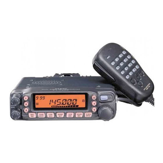
Dual Band FM Transceiver
FT-7800R
Technical Supplement
©
2003 VERTEX STANDARD CO., LTD.
Introduction
This manual provides technical information necessary for servicing the FT-7800R Transceiver.
Servicing this equipment requires expertise in handling surface-mount chip components. Attempts by non-qualified
persons to service this equipment may result in permanent damage not covered by the warranty, and may be illegal in
some countries.
Two PCB layout diagrams are provided for each double-sided circuit board in the transceiver. Each side of thr board is
referred to by the type of the majority of components installed on that side ("leaded" or "chip-only"). In most cases one
side has only chip components, and the other has either a mixture of both chip and leaded components (trimmers, coils,
electrolytic capacitors, ICs, etc.), or leaded components only.
While we believe the technical information in this manual to be correct, Vertex Standard assumes no liability for dam-
age that may occur as a result of typographical or other errors that may be present. Your cooperation in pointing out any
inconsistencies in the technical information would be appreciated.
Specifications ................................................ A-1
Exploded View & Miscellaneous Parts ..... B-1
Block Diagram ................................................ C-1
Circuit Description ....................................... D-1
Alignment ....................................................... E-1
( EH016M90A )
Contents
Board Unit (Schematics, Layouts & Parts)
Main Unit................................................. F-1
Panel Unit ............................................. G-1
Ch Unit ..................................................... H-1
VERTEX STANDARD CO., LTD.
4-8-8 Nakameguro, Meguro-Ku, Tokyo 153-8644, Japan
VERTEX STANDARD
US Headquarters
10900 Walker Street, Cypress, CA 90630, U.S.A.
YAESU EUROPE B.V.
P.O. Box 75525, 1118 ZN Schiphol, The Netherlands
YAESU UK LTD.
Unit 12, Sun Valley Business Park, Winnall Close
Winchester, Hampshire, SO23 0LB, U.K.
VERTEX STANDARD HK LTD.
Unit 5, 20/F., Seaview Centre, 139-141 Hoi Bun Road,
Kwun Tong, Kowloon, Hong Kong
Advertisement
Table of Contents

Related Manuals for Yaesu FT-7800R


Summary of Contents for Yaesu FT-7800R
- Page 1 2003 VERTEX STANDARD CO., LTD. Introduction This manual provides technical information necessary for servicing the FT-7800R Transceiver. Servicing this equipment requires expertise in handling surface-mount chip components. Attempts by non-qualified persons to service this equipment may result in permanent damage not covered by the warranty, and may be illegal in some countries.
-
Page 2: Specifications
Specifications Frequency Range: RX: 108.000 - 520.000 MHz, 700.000 - 999.995 MHz (Cellular Blocked) TX: 144.000 - 148.000 MHz or 144.000 - 146.000 MHz, 430.000 - 450.000 MHz or 430.000 - 440.000 MHz Channel Steps: 5/10/12.5/15/20/25/50/100 kHz Modes of Emission: F3E, F2D, F2A Antenna Impedance: 50 Ohms, unbalanced (Antenna Duplexer built-in) - Page 3 Exploded View & Miscellaneous Parts Œ ’ R8139500 Œ LABEL SCREW LIST Œ CS1804001 No. VXSTD P/N DESCRIPTION QTY. ’ ’ CASE (W/ NYLON NET) Œ U31208007 OVAL HEAD SCREW M2.6X8B Œ Œ U44308002 TAPTITE SCREW M3X8NI ’ Ž U03310002 SEMS SCREW ASM3X10NI RA02132A0...
- Page 4 Exploded View & Miscellaneous Parts...
- Page 5 Block Diagram...
- Page 6 Block Diagram...
-
Page 7: Circuit Description
Circuit Description The detected audio passes through the de-emphasis net- VHF Reception work, a low-pass filter consisting of Q1028 (NJM2902V) The incoming VHF signal is passed through a low-pass and associated circuitry, and a high-pass filter consisting filter network, antenna switching diodes D1074 (RLS135), of Q1028 (NJM2902V) and associated circuitry. -
Page 8: Pll Circuit
Circuit Description UHF Transmit Signal Path PTT Circuit The adjusted speech signal from Q1040 (NJM2902V) is When the PTT switch is pressed, pin 8 of sub CPU Q2001 delivered to UHF VCO Q1072 (2SC5006) which frequen- (M38223E) goes “high”, which send the “PTT” command cy modulates the transmitting VCO made up of D1046 to main CPU Q1065 (M3826AEFGP). - Page 9 Alignment Introduction and Precautions Required Test Equipment The FT-7800R has been carefully aligned at the factory The following test equipment (and thorough familiarity for the specified performance across the 144 MHz and 430 with its correct use) is necessary for complete realignment.
- Page 10 Front-end has a broad bandwidth. Therefore, prior to adjustment you must adjust the DIAL knob to set the Alignment of the FT-7800R is performed using a front- frequency to the middle of the band, in step 2, so you panel software-based procedure. To perform alignment can set peak in the DC voltmeter's deflection in the of the transceiver, it must first be placed in the “Align-...
- Page 11 Alignment TX Power Output TX Deviation 1. Tune the frequency to 440.050 MHz, then set the Trans- 1. Tune the frequency to 440.050 MHz, then set the Trans- mit Power Level to “LOW.” mit Power Level to “LOW.” 2. Press the [ BAND ( SET )] key while pressing and hold- 2.
- Page 12 7. Tune the frequency to 146.050 MHz. CTCSS TX Deviation 8. Inject a 146.050 MHz signal at a level of –5 dBµ (with 1. Tune the frequency to 440.050 MHz, then activate the 1 kHz modulation @±3.5 kHz deviation) from the RF CTCSS Encoder with a “100 Hz”...
- Page 13 MAIN Unit Circuit Diagram Q1034 Pin 2: 8.33 V 1.42 V Pin 14: 8.40 V AM: 2.03 V Pin 15: 3.57 V 2.00 V 2.00 V Pin 16: 3.27 V AM: 3.74 V [+15.5 dBµ] [+1.4 dBµ] [+18.8 dBµ] 1.48 V 1.10 V [–4.3 dBµ] 0 ~ 4.90 V...
- Page 14 MAIN Unit Note...
-
Page 15: Main Unit
MAIN Unit Parts Layout (Side A) M3826AEFGP BU2090FS BU4066BCFV (Q1065) (Q1059) (Q1039) M51132FP NJM2902V (Q1034) (Q1040) MB15A022PFV1 (Q1070) TA31136FN (Q1023) RD70HVF1 (Q1087) 2SA1774 (FR) 2SB1301 (ZQ) LA4425A (Q1069) (Q1043) (Q1035) 2SC4400 (RT4) 2SK2596 (BX) IMT17 (T17) (Q1016) (Q1084) (Q1058) 2SC4617 (BR) (Q1019, 1020, 1029, 1030, 1047, 1064, 1071) - Page 16 MAIN Unit Parts Layout (Side B) 2SB1201S AT24C256 NJM2902V (Q1044) (Q1053) (Q1028, 1031) NJM2904V (Q1081) 2SC4400 (RT4) 2SD1664 (DA) 3SK296ZQ (ZQ) (Q1022) (Q1085) (Q1001, 1002, 1008, 1009, 1010) 2SC4617 (BR) (Q1017, 1018, 1021, 1041, 1051, 1052) 2SC5006 (24) (Q1072, 1073) 2SC5374 (NA) (Q1011, 1076, 1077) DTA144EE (16)
-
Page 17: Parts List
MAIN Unit Parts List DESCRIPTION VALUE TOL. MFR'S DESIG VXSTD P/N VERS. LOT SIDE LAY ADR PCB with Components CS1803001 USA A2U CS1803004 EXP A1 CS1803005 EXP A2 CS1803006 EXP A3 CS1803007 EXP B1 CS1803008 EXP B2 CS1803009 EXP B3 CS1803010 EXP C1 CS1803011... - Page 18 MAIN Unit Parts List DESCRIPTION VALUE TOL. MFR'S DESIG VXSTD P/N VERS. LOT SIDE LAY ADR C 1053 CHIP CAP. GRM36CH080B50PT K22178295 C 1054 CHIP CAP. 1.5pF GRM36CK1R5B50PT K22178288 C 1054 CHIP CAP. 1.5pF GRM36CK1R5B50PT K22178288 C 1054 CHIP CAP. 1.5pF GRM36CK1R5B50PT K22178288...
- Page 19 MAIN Unit Parts List DESCRIPTION VALUE TOL. MFR'S DESIG VXSTD P/N VERS. LOT SIDE LAY ADR C 1123 CHIP CAP. 0.001uF GRM36B102K50PT K22178809 C 1124 CHIP CAP. 0.01uF GRM36B103K16PT K22128804 C 1125 CHIP CAP. 0.01uF GRM36B103K16PT K22128804 C 1126 CHIP CAP. 0.001uF GRM36B102K50PT K22178809...
- Page 20 MAIN Unit Parts List DESCRIPTION VALUE TOL. MFR'S DESIG VXSTD P/N VERS. LOT SIDE LAY ADR C 1200 CHIP CAP. 0.0047uF GRM36B472K25PT K22148830 C 1201 CHIP CAP. 0.001uF GRM36B102K50PT K22178809 C 1202 CHIP CAP. 0.1uF GRM36B104K10PT K22108802 C 1203 CHIP CAP. GRM39F105Z10PT K22105001 C 1204...
- Page 21 MAIN Unit Parts List DESCRIPTION VALUE TOL. MFR'S DESIG VXSTD P/N VERS. LOT SIDE LAY ADR C 1280 CHIP CAP. 0.001uF GRM36B102K50PT K22178809 C 1281 CHIP CAP. GRM39F105Z10PT K22105001 C 1283 CHIP CAP. 47pF GRM36CH470J50PT K22178228 C 1284 CHIP CAP. 0.001uF GRM36B102K50PT K22178809...
- Page 22 MAIN Unit Parts List DESCRIPTION VALUE TOL. MFR'S DESIG VXSTD P/N VERS. LOT SIDE LAY ADR C 1356 CHIP CAP. 0.001uF GRM36B102K50PT K22178809 C 1358 CHIP CAP. 0.001uF GRM36B102K50PT K22178809 C 1359 CHIP CAP. GRM36CH070B50PT K22178294 C 1361 CHIP CAP. 0.001uF GRM36B102K50PT K22178809...
- Page 23 MAIN Unit Parts List DESCRIPTION VALUE TOL. MFR'S DESIG VXSTD P/N VERS. LOT SIDE LAY ADR C 1414 CHIP CAP. 56pF GRM36CH560J50PT K22178230 VER. C2 C 1414 CHIP CAP. 56pF GRM36CH560J50PT K22178230 VER. C3 C 1414 CHIP CAP. 56pF GRM36CH560J50PT K22178230 VER.
- Page 24 MAIN Unit Parts List DESCRIPTION VALUE TOL. MFR'S DESIG VXSTD P/N VERS. LOT SIDE LAY ADR C 1435 CHIP CAP. GRM36CH050B50PT K22178292 VER. C3 C 1435 CHIP CAP. GRM36CH050B50PT K22178292 VER. D1 C 1435 CHIP CAP. GRM36CH050B50PT K22178292 VER. D2 C 1435 CHIP CAP.
- Page 25 MAIN Unit Parts List DESCRIPTION VALUE TOL. MFR'S DESIG VXSTD P/N VERS. LOT SIDE LAY ADR C 1462 CHIP CAP. GRM36CH060B50PT K22178293 VER. B1 C 1462 CHIP CAP. GRM36CH060B50PT K22178293 VER. B2 C 1462 CHIP CAP. GRM36CH060B50PT K22178293 VER. B3 C 1462 CHIP CAP.
- Page 26 MAIN Unit Parts List DESCRIPTION VALUE TOL. MFR'S DESIG VXSTD P/N VERS. LOT SIDE LAY ADR D 1003 DIODE HVC350B-TRF G2070596 D 1004 DIODE HVC350B-TRF G2070596 D 1005 DIODE HVC131TRF G2070676 D 1006 DIODE HVC131TRF G2070676 D 1007 DIODE HVC131TRF G2070676 D 1009 DIODE...
- Page 27 MAIN Unit Parts List DESCRIPTION VALUE TOL. MFR'S DESIG VXSTD P/N VERS. LOT SIDE LAY ADR D 1069 DIODE HSC277TRF G2070584 VER. A2 D 1069 DIODE HSC277TRF G2070584 VER. A3 D 1069 DIODE HSC277TRF G2070584 VER. B1 D 1069 DIODE HSC277TRF G2070584 VER.
- Page 28 MAIN Unit Parts List DESCRIPTION VALUE TOL. MFR'S DESIG VXSTD P/N VERS. LOT SIDE LAY ADR L 1032 M.RFC 0.0047uH TFL0816-4N7 L1690487 L 1033 M.RFC 0.0047uH TFL0816-4N7 L1690487 L 1034 M.RFC 0.0047uH TFL0816-4N7 L1690487 L 1035 M.RFC 0.0047uH TFL0816-4N7 L1690487 L 1036 M.RFC 0.022uH...
- Page 29 MAIN Unit Parts List DESCRIPTION VALUE TOL. MFR'S DESIG VXSTD P/N VERS. LOT SIDE LAY ADR Q 1012 TRANSISTOR 2SC5277-D2-TL G3352778B Q 1013 TRANSISTOR 2SC5006-T1 G3350068 Q 1014 TRANSISTOR 2SC5006-T1 G3350068 Q 1016 TRANSISTOR 2SC4400-3-TL G3344008C Q 1017 TRANSISTOR 2SC4617 TL R G3346178R Q 1018 TRANSISTOR...
- Page 30 MAIN Unit Parts List DESCRIPTION VALUE TOL. MFR'S DESIG VXSTD P/N VERS. LOT SIDE LAY ADR R 1004 CHIP RES. 1/16W 0.5% RR0510P-103-D J24189143 R 1005 CHIP RES. 1/16W RMC1/16S 473JTH J24189045 R 1007 CHIP RES. 1/16W 0.5% RR0510R-153-D J24189147 R 1007 CHIP RES.
- Page 31 MAIN Unit Parts List DESCRIPTION VALUE TOL. MFR'S DESIG VXSTD P/N VERS. LOT SIDE LAY ADR R 1074 CHIP RES. 560k 1/16W RMC1/16S 564JTH J24189058 R 1075 CHIP RES. 1/16W RMC1/16S 101JTH J24189013 R 1076 CHIP RES. 1/16W RMC1/16S 102JTH J24189025 R 1077 CHIP RES.
- Page 32 MAIN Unit Parts List DESCRIPTION VALUE TOL. MFR'S DESIG VXSTD P/N VERS. LOT SIDE LAY ADR R 1153 CHIP RES. 1/16W RMC1/16S 103JTH J24189037 R 1154 CHIP RES. 220k 1/16W RMC1/16S 224JTH J24189053 R 1155 CHIP RES. 220k 1/16W RMC1/16S 224JTH J24189053 R 1156 CHIP RES.
- Page 33 MAIN Unit Parts List DESCRIPTION VALUE TOL. MFR'S DESIG VXSTD P/N VERS. LOT SIDE LAY ADR R 1228 CHIP RES. 1/16W RMC1/16S 221JTH J24189017 R 1229 CHIP RES. 1/16W RMC1/16S 221JTH J24189017 R 1230 CHIP RES. 1/16W RMC1/16S JPTH J24189070 R 1231 CHIP RES.
- Page 34 MAIN Unit Parts List DESCRIPTION VALUE TOL. MFR'S DESIG VXSTD P/N VERS. LOT SIDE LAY ADR R 1309 CHIP RES. 390k 1/16W RMC1/16S 394JTH J24189056 R 1310 CHIP RES. 820k 1/16W RMC1/16S 824JTH J24189060 R 1311 CHIP RES. 1.5M 1/16W RMC1/16S 155JTH J24189063 R 1312...
- Page 35 MAIN Unit Parts List DESCRIPTION VALUE TOL. MFR'S DESIG VXSTD P/N VERS. LOT SIDE LAY ADR R 1383 CHIP RES. 1/16W RMC1/16S 183JTH J24189040 R 1384 CHIP RES. 4.7k 1/16W RMC1/16S 472JTH J24189033 R 1385 CHIP RES. 1/16W RMC1/16S 183JTH J24189040 R 1386 CHIP RES.
- Page 36 MAIN Unit Parts List DESCRIPTION VALUE TOL. MFR'S DESIG VXSTD P/N VERS. LOT SIDE LAY ADR R 1432 CHIP RES. 1/16W RMC1/16S 470JTH J24189009 R 1433 CHIP RES. 1/16W RMC1/16S 101JTH J24189013 R 1434 CHIP RES. 1/16W RMC1/16S JPTH J24189070 USA A2 R 1434 CHIP RES.
- Page 37 MAIN Unit Parts List DESCRIPTION VALUE TOL. MFR'S DESIG VXSTD P/N VERS. LOT SIDE LAY ADR R 1467 CHIP RES. 1/16W RMC1/16S 820JTH J24189012 R 1468 CHIP RES. 1/16W RMC1/16 102JATP J24185102 R 1469 CHIP RES. 1/16W RMC1/16 102JATP J24185102 R 1470 CHIP RES.
- Page 38 MAIN Unit Parts List DESCRIPTION VALUE TOL. MFR'S DESIG VXSTD P/N VERS. LOT SIDE LAY ADR R 1488 CHIP RES. 1/16W RMC1/16S 103JTH J24189037 R 1489 CHIP RES. 1/16W RMC1/16S 103JTH J24189037 R 1490 CHIP RES. 1/16W RMC1/16S 103JTH J24189037 R 1491 CHIP RES.
- Page 39 PANEL Unit Circuit Diagram 1.58 V 5.00 V 3.15 V 5.00 V DIM 1: 4.36 V DIM OFF: 0 V DIM 1: 7.26 V DIM OFF: 8.45 V 8.68 V 3.57 V 8.90 V...
-
Page 40: Panel Unit
PANEL Unit Parts Layout (Side A) Common Segment (DS2001) Parts Layout (Side B) M38223M4M LC75821E NJM2904V (Q2002) (Q2011) (Q2001) 2SA1774 (FR) 2SB1132 (BA) DTC144EE (26) (Q2004) (Q2006) (Q2005) DTA144EE (16) NJM78L05 (8C) UMW1 (W1) (Q2012) (Q2003) (Q2007) HZM27WA (27A) (D2011, 2014) - Page 41 PANEL Unit Parts List DESCRIPTION VALUE TOL. MFR'S DESIG VXSTD P/N VERS. LOT SIDE LAY ADR PCB with Components CB2349001 CB2349003 CB2349004 Printed Circit Board AH016M000 FR0111800 C 2001 CHIP CAP. 47pF GRM36CH470J50PT K22178228 C 2002 CHIP CAP. 47pF GRM36CH470J50PT K22178228 C 2003 CHIP CAP.
- Page 42 PANEL Unit Parts List DESCRIPTION VALUE TOL. MFR'S DESIG VXSTD P/N VERS. LOT SIDE LAY ADR Q 2004 TRANSISTOR 2SA1774 TL R G3117748R Q 2005 TRANSISTOR DTC144EE TL G3070075 Q 2006 TRANSISTOR 2SB1132 T100 Q G3211327Q Q 2007 TRANSISTOR UMW1 TR G3070078 Q 2011 NJM2904V-TE1...
- Page 43 PANEL Unit Parts List DESCRIPTION VALUE TOL. MFR'S DESIG VXSTD P/N VERS. LOT SIDE LAY ADR R 2071 CHIP RES. 1/16W RMC1/16S 820JTH J24189012 R 2072 CHIP RES. 1/16W RMC1/16S 563JTH J24189046 R 2073 CHIP RES. 1/16W RMC1/16S 821JTH J24189024 R 2074 CHIP RES.
- Page 44 PANEL Unit Parts List Note DESCRIPTION VALUE TOL. MFR'S DESIG VXSTD P/N VERS. LOT SIDE LAY ADR...
- Page 45 CH Unit Circuit Diagram Parts Layout Side A SideB Parts List DESCRIPTION VALUE TOL. MFR'S DESIG VXSTD P/N VERS. LOT SIDE LAY ADR PCB with Components CB2350001 Printed Circuit Board AH016M000 FR0111900 J 3001 CONNECTOR NTC-623PCBL6-B P1091107 S 3001 ROTARY ENCODER EC11B15202AA Q9000804...
- Page 46 CH Unit Note...
- Page 48 Copyright 2003 VERTEX STANDARD CO., LTD. All rights reserved. No portion of this manual may be reproduced without the permission of VERTEX STANDARD CO., LTD.
Need help?
Do you have a question about the FT-7800R and is the answer not in the manual?
Questions and answers