Table of Contents
Advertisement
Quick Links
Advertisement
Table of Contents

Related Manuals for Sony MDS-B5


Summary of Contents for Sony MDS-B5
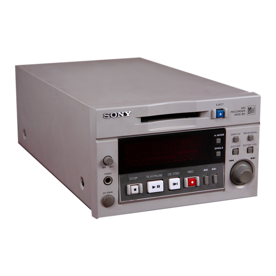
- Page 1 MDS-B5 SERVICE MANUAL US Model Canadian Model AEP Model UK Model Model Name Using Similar Mechanism MDS-B3 MD Mechanism Type MDM-2BL Base Unit Type MBU-2BL Optical Pick-up Type KMS-210A/J-N SPECIFICATIONS — Continued on next page — MD RECORDER MICROFILM — 1 —...
- Page 2 — 2 —...
- Page 3 REPLACE THESE COMPONENTS WITH SONY PARTS FONCTIONNEMENT. NE REMPLACER CES COMPOSANTS WHOSE PART NUMBERS APPEAR AS SHOWN IN THIS QUE PAR DES PIÈCES SONY DONT LES NUMÉROS MANUAL OR IN SUPPLEMENTS PUBLISHED BY SONY. SONT DONNÉS DANS CE MANUEL OU DANS LES SUPPLÉMENTS PUBLIÉS PAR SONY.
-
Page 4: Table Of Contents
TABLE OF CONTENTS 1. GENERAL 4. ELECTRICAL ADJUSTMENTS 2-1. Front Panel ................5 4-1. Precautions for Checking Laser Diode Emission ....39 4-2. Precautions for Use of optical pickup (KMS-210A) ..39 2-2. Rear Panel ................6 4-3. Precautions for Adjustments ..........39 2-3. -
Page 5: General
SECTION 1 This section is extracted from instruction manual. GENERAL — 5 —... - Page 6 — 6 —...
- Page 7 — 7 —...
- Page 8 — 8 —...
- Page 9 — 9 —...
- Page 10 — 10 —...
- Page 11 — 11 —...
- Page 12 — 12 —...
- Page 13 — 13 —...
- Page 14 — 14 —...
- Page 15 — 15 —...
- Page 16 — 16 —...
- Page 17 — 17 —...
- Page 18 — 18 —...
- Page 19 — 19 —...
- Page 20 — 20 —...
- Page 21 — 21 —...
- Page 22 — 22 —...
- Page 23 — 23 —...
- Page 24 — 24 —...
- Page 25 — 25 —...
- Page 26 — 26 —...
- Page 27 — 27 —...
- Page 28 — 28 —...
- Page 29 — 29 —...
- Page 30 — 30 —...
- Page 31 — 31 —...
- Page 32 — 32 —...
-
Page 33: Front Panel
SECTION 2 DISASSEMBLY Note: Follow the disassembly procedure in the numerical order given. 2-1. CASE AND FRONT PANEL ASSEMBLY 1 Two screws (+B4x8) 3 Screw (+BVTT3x8) 4 Case 2 Two screws (+B4x8) 6 Wire (Flat type) (16 core) 7 Front panel assembly 5 Two screws (+BVTT3x8) 2-2. -
Page 34: Mechanism Deck
2-3. MECHANISM DECK 3 Rotate the pulley (BD) in the direction 4 Two screws of arrow A , and slide the slider (M) 1 Two screws (+B2.6x18) assembly in the direction of arrow B . (+B2.6x18) (As the stopper catches halfway, lightly 5 Two collares push up the stopper in the fig. -
Page 35: Base Unit (Mbu-2Bl), Loading Motor Assembly
2-5. BASE UNIT (MBU-2BL), LOADING MOTOR ASSEMBLY 4 Belt (BD) 5 Two screws (+B2.6x5) 6 Connector (CN192) 1 Screw (+BVTP3x6) 7 Loading motor assembly 3 MD base unit (MBU-2BL) 2 Two screws (+BVTP3x6) 2-6. SLIDER ASSEMBLY MOUNTING 4 Move the slider assembly in arrow direction B , and lock it to the lever (SLM). - Page 36 SECTION 3 TEST MODE 3-1. Setting the Test Mode While pressing the AMS knob, turn POWER switch on, and release the AMS knob. 3-2. Exiting the Test Mode Turn POWER switch off. 3-3. Basic Operations of the Test Mode All operations are performed using the AMS knob, ENTER/YES button, and EDIT/NO button. The functions of these buttons are as follows.
- Page 37 3-4-2. Operating the Continuous Recording Mode 1. Entering the continuous recording mode 1 Set the MO disc in the unit. 2 Rotate the AMS knob and display “CREC MODE”. 3 Press the ENTER/YES button to change the display to “CREC IN”. 4 When access completes, the display changes to “CREC ( )”.
- Page 38 3-6. Test Mode Displays Each time the DISPLAY button is pressed, the display changes in the following order. MODE displaynError rate displaynAddress display 1. MODE display Displays “TEMP ADJUST”, “CPLAY MODE”, etc. 2. Error rate display Error rates are displayed as follows. C1 = AD = C1 = : Indicates C1 error...
-
Page 39: Electrical Adjustments
SECTION 4 ELECTRICAL ADJUSTMENTS 4-1. Precautions for Checking Laser Diode 4-3. Precautions for Adjustments Emission 1) When replacing the following parts, perform the adjustments and checks with ® in the order shown in the following table. To check the emission of the laser diode during adjustments, never view directly from the top as this may lose your eye-sight. -
Page 40: Temperature Compensation Offset Adjustment
4-5. Temperature Compensation Offset Adjustment 4-6. Laser Power Adjustment Save the temperature data at that time in the non-volatile memory as Connection : Laser power 25 ˚C reference data. meter Note : 1. Usually, do not perform this adjustment. 2. Perform this adjustment in an ambient temperature of 22 ˚C to 28 ˚C. -
Page 41: Traverse Adjustment
4-7. Traverse Adjustment 11. Rotate the AMS knob until the waveform of the oscilloscope moves closer to the specified value. In this adjustment, waveform varies at intervals of approx. 3%. Connection : Adjust the waveform so that the specified value is satisfied as Oscilloscope much as possible. -
Page 42: Focus Bias Adjustment
4-8. Focus Bias Adjustment 4-9. Error Rate Check 4-9-1. CD Error Rate Check Adjusting Method : Checking Method : 1. Load a continuously recorded disc (Refer to “4-4. Creating MO 1. Load a test disc TDYS-1. Continuously Recorded Disc”.). 2. Rotate the AMS knob and display “CPLAY MODE”. 2. -
Page 43: Adjusting Points And Connecting Points
SECTION 5 DIAGRAMS 4-11. Adjusting Points and Connecting Points 5-1. CIRCUIT BOARDS LOCATION [BD BOARD] (COMPONENT SIDE) ADIO board PIO board POWER board D101 DUP IN board HP board 232C board DUP OUT board JACK board DIG board IC191 D IN board [BD BOARD] (CONDUCTOR SIDE) D OUT board A IN board... -
Page 44: Block Diagrams
MDS-B5 5-2. BLOCK DIAGRAMS SCTX SQSY —BD SECTION— DIGITAL SIGNAL PROCESSOR, DOUT DIGITAL SERVO SIGNAL PROCESSOR, EFM/ACIRC ENCODER/DECODER IC121 EEP ROM 51 52 49 53 IC171 Q181,182 SQSY HR901 OVER WRITE OVER HEAD DIDT HEAD DRIVE SUBCODE WRITE DRIVE DIGITAL... -
Page 45: Digital Section
MDS-B5 —DIGITAL SECTION— (Page 49) ABCK ABCK REMOTE ALRCK ALRCK SECTION DODT ADIN DUPLICATION (Page 51) DOUT SECTION SAMPLING RATE INTERFACE RECEIVER SWITCH CONVERTER DIG IN/OUT IC410 IC411 IC409 IC871 D-RAM DATAO DATAI IC402 DATAO AVOCK BCKO BCKI LRCKO LRCK... -
Page 46: Duplication Section
MDS-B5 —DUPLICATION SECTION— HIGH SPEED DUBBING DIGITAL OUT RECEIVER IC901 IC951 OUTACK D-RAM IC408 OUTXABS DQ1 - DQ4 A0 - A9 1 2 18 19 4 5 21 20 5 - 9 11 - 15 OUTDATA 68 - 71 67 66 62 61... -
Page 47: Remote Section
LOADING MOTOR DRIVE I/O EXPANDER IC309 IC304 —REMOTE SECTION— LOUT (Page 47) DIGITAL SECTION LEVEL METER SECTION IC305 LDON (Page 46) SYSTEM CONTROL BUFFER IC301 (2/2) IC314 DODT DATA RQEN ABCK KDATA RERES DUPLICATION ALRCK LRCK SECTION XRES (Page 49) DOUTMT AESDT AES/EBU TRANSMITTER... -
Page 48: Power Section
MDS-B5 — POWER SECTION — POWER TRANSFROMER FL601 -32V REG IC11 -32V +10V IC955 (DUP OUT) IC956 (DUP IN) +5V/+6V REG REF. VOL. DISP5V +5V REG IC507 +5V REG +6V REG IC191 IC12 (BD) +5V REG IC14 DIG5V POWER B.UP5V... -
Page 59: Ic Pin Functions
5-13. IC PIN FUNCTIONS • IC121 Digital signal procesor, digital servo processor, EFM/ACIRC encoder/decoder (CXD2535CR) • IC101 RF Amplifier (CXA1981AR) Pin No. Pin Name Function Pin No. Pin Name Function 11.2896 MHz clock output (MCLK) (Not used) FS256 Middle point voltage (2.5V) generation output Output of FOK signal to system controller (IC301) 2 to 7 A to F... - Page 60 Pin No. Function Pin Name WFCK clock (7.35 kHz) signal output WFCK (Playback: EFM decoder PLL. Recording: EFM encoder PLL) (Not used) GTOP “H”: Opens playback EFM frame sync protection window (Not used) “H”: Playback EFM sync and interpolation protection timing match (Not used) EFM decoder PLL clock output (98 fs=4.3218 MHz) XPLCK Falling edge and EFM signal edge match (Not used)
- Page 61 Pin No. Pin Name Function TEST1 Test pin (Fixed at “L”) Input of ADIP dual FM signal from CXA1981AR (IC101) (22.05 kHz ±1 kHz) ADFG (TTL Schmidt input) TS25 Test pin (Fixed at “L”) LDDR Laser APC signal output TRDR Tracking servo drive signal output (–) TFDR Tracking servo drive signal output (+)
-
Page 62: Ic301 System Control (M30600E8Fp)
• IC301 System Control (M30600E8FP) Pin No. Pin Name Function Function SHCK Jog detection input from the CXD2535CR. Focus OK input from the CXD2535CR. C1 error test output ADER, C2 ADER, C2 error test output SQSY SUBQ/ATIP sync input from the CXD2535CR. SIRCS Wired remote control input PDOWN... - Page 63 Function Pin No. Pin Name External data bus hold input (Fixed to “H”.) XHOLD External data bus hold output XHLDA Internal clock output (4.3 MHz) BCLK External data bus read request output External data bus odd address write request output XWRH External data bus even address write request output XWRL...
-
Page 64: Ic401 Shock-Proof Memory Controller, Atrac Encoder/Decoder (Cxd2536Cr)
• IC401 Shock-Proof Memory Controller, ATRAC Encoder/Decoder (CXD2536CR) Pin No. Pin Name Function — Power supply (+5V) SWDT Input of write data signal from system controller (IC301) Input of serial clock signal from system controller (IC301) XLAT Input of serial latch signal from system controller (IC301) SRDT Output of read data signal to system controller (IC301) SENSE... - Page 65 Pin No. Pin Name Function 48, 49 A11, A10 Output of address signal to RAM (IC402) — Ground — Power supply (+5V) 52 to 55 A03 to A00 Output of address signal to RAM (IC402) 56 to 60 A04 to A08 Output of address signal to RAM (IC402) Output of output enable control signal to RAM (IC402) XCAS...
-
Page 66: Ic407 Shock-Proof Memory Controller, Atrac Encoder/Decoder (Cxd2536Cr)
• IC407 Shock-Proof Memory Controller, ATRAC Encoder/Decoder (CXD2536CR) Pin No. Pin Name Function — Power supply (+5V) SWDT Input of write data signal from system controller (IC301) Input of serial clock signal from system controller (IC301) XLAT Input of serial latch signal from system controller (IC301) SRDT Output of read data signal to system controller (IC301) SENSE... - Page 67 Pin No. Pin Name Function 48, 49 A11, A10 Address signal output (Not used) — Ground — Power supply (+5V) 52 to 55 A03 to A00 Output of address signal to RAM (IC408) 56 to 60 A04 to A08 Output of address signal to RAM (IC408) Output of output enable control signal to RAM (IC408) XCAS Output of column address strobe signal to RAM (IC408)
-
Page 68: Ic409 Sampling Rate Converter (Cxd8517Q)
• IC409 Sampling Rate Converter (CXD8517Q) Pin No. Pin Name Function Data input DATAI Input data fs word clock input (Schemidt) LRCKI Input data bit clock input BCKI Input data format setting input 0 (Fixed at “L”) Input data format setting input 1 (Fixed at “L”) +5V power supply —... -
Page 69: Ic Block Diagrams
5-14. IC BLOCK DIAGRAMS IC11 M5293L REFERENCE VOLTAGE REFERENCE – ON/OFF VOLTAGE OVERHEAT OVERCURRENT PROTECTION LIMITTER IC15 BA3960 REF. VOLTAGE – – IC16 SN74HCU04ANS — 100 —... - Page 70 IC121 CXD2535CR 74 73 72 71 69 68 67 66 65 63 62 61 60 58 57 56 55 54 53 52 51 50 DVSS DIN PLL DIPO (22 MHz) 34 MHz SE 76 ANALOG MUX COMP TEST2 TE 77 MVC1 OP AMP TENV 78...
- Page 71 IC171 X24C08SC7000 TEST INPUT START CYCLE H.V. GENERATION TIMING START & CONTROL STOP LOGIC CONTROL LOGIC E PROM XDEC 32 x 32 LOAD WORD ADDRESS COUNTER YDEC DATA REGISTER IC191, 507 L88MS05T-FA-TL OVERVOLTAGE PROTECTOR REFERENCE START VOLTAGE VOLTAGE ERROR ON / OFF CURRENT CONTROL LIMITTER...
- Page 72 IC201 CXA8027N-ELL2000 OVER ROTOR HEAT POSITION PROTECT DETECT SOFT OUTPUT START TIMING DRIVER SWITCHING DRIVE CONTROL CONTROL DRIVE BUFFER EXOR IC304, 306 M66500FP PORT F PORT G PORT C (8 BIT) (4 BIT) (HIGHT 4 BIT) PORT C (LOW 4 BIT) PORT E (8 BIT) DATA BUS...
- Page 73 IC309 BA6287F-T1 IC302 AT29C1024-70 OUT1 Y DECODER OUT2 X DECODER DRIVER DRIVER VREF CONTROL LOGIC POWER SAVE IC310 M62005FP OE ,CE AND WE LOGIC INTERRUPT SIGNAL – GENERATOR RESET SIGNAL – GENERATOR IC311, 314 TC7W08FU IC305 MSM6338MS-K 0 DB DATA 0 DB 16 BIT 0 DB...
- Page 74 IC313 M66230FP RECEIVER BUFFER BAUD RECEIVER 4byte FIFO GENERATOR SAMPLING RECEIVER CONTROL, ERROR STATUS CLOCK DETECT CIRCUIT (CRC etc.) REGISTER DIVIDER TRANSMITTER CIRCUIT BUFFER TRANSMITTER 4byte FIFO TRANSFER TRANSMITTER CONTROL, ERROR CLOCK DETECT CODE GENERATE CIRCUIT COMMAND (CRC etc.) REGISTER READ/WRITE DATA BUS BUFFER CONTROL CIRCUIT...
- Page 75 IC401, 407 CXD2536CR SWDT SCLK ATRAC Encoder/Decoder XLAT SRDT SENS SMD0 SMD1 Memory Data Controller I/F Memory XINT RCPB XRAS WRMN ATRAC Encoder/Decoder I/F TST0 XCAS TST1 DI Block TST2 RAM R/W Controller XRST CD-ROM Encoder/Decoder TST3 TST4 Clock Generator TST5 IC404 TC74VHC74FS —...
- Page 76 IC410 LC89051V-TLM IC413, 506 TCW74FU ERROR MUTE OUT DIN1 DATA DECODE LOCK ERROR DIN2 INPUT BLOCK DETECT DOUT DATAO BIT DETECT SUB-Q DETECT TIMING MYCOM INTERFACE LRCK IC405, 703, 873 TC7WU04F FS128 CKOUT CKSEL DQSY SRDT SWDT XLAT XMODE SCLK TEST AVOCK TEST2...
- Page 77 IC501 CXD8566M-T6 VOLTAGE REFERENCE DECIMATION LOW CUT MODULATOR FILTER FILTER DECIMATION LOW CUT MODULATOR FILTER FILTER TIMING CIRCUIT IC502 CXA8054M-T6 – – – – IC503 CXD8567AM-T6 INIT D Vdd 2 SYSM L1 (+) A Vdd L SHIFT L2 (+) LATCH A Vss L 256FSO X Vss...
- Page 78 IC601 M66004FP 64 - 61 59 - 33 (35BIT x 16) DECODER CODE SELECT INDICATION SEGMENT CODE/COMMAND INDICATION INDICATION DIGIT OUTPUT CODE OUTPUT CONTROL CONTROL CONTROLLER CIRCUIT CODE RESISTOR CIRCUIT RESISTOR CIRCUIT (8BIT x 16) WRITE DECODER (35BIT x 16) WRITE SERIAL OUTPUT...
- Page 79 IC901 CXD8633Q OUTARQ XARQ36 DTO36 OUTDATA SERIAL BUS SELECTOR DTI36 OUTXABS XABS36 OUTACK DUPLICATON ACK36 CONTROLLER XRES INARQ RELES AUDIO DATA RQEN INDATA CONTROLLER INXABS DOUT AXBCK INACK IC953 AM26C32CNS IC951 AM26C31CNS — 110 —...
-
Page 80: Exploded Views
4-983-735-01 LID (CHASSIS) 4-983-730-01 BUTTON (FF.REW) 1-777-238-11 WIRE (FLAT TYPE)(16 CORE) 4-983-729-01 BUTTON (SHORT) * 15 A-4699-172-A DISP BOARD, COMPLETE 4-942-568-01 EMBLEM (NO.5), SONY 4-989-820-01 CAP (MINI-DIN) 3-668-009-02 PIN, PUSH BUTTON * 17 4-956-134-01 HOLDER (FL TUBE) 3-567-099-01 SPRING, COMPRESSION... -
Page 81: Chassis Section
6-2. CHASSIS SECTION not supplied #4 #4 (including not supplied MDM-2BL 65 66 not supplied not supplied not supplied Supplied with RV805 The components identified by mark ! or dotted line with mark ! are critical for safety. Replace only with part number specified. -
Page 82: Back Panel Section
6-3. BACK PANEL SECTION not supplied supplied with J701 Ref. No. Part No. Description Remark Ref. No. Part No. Description Remark 3-906-061-01 SPACER (SW) * 110 1-662-432-11 232C BOARD * 102 X-4801-204-0 TERMINAL ASSY 2-251-642-01 GUARD, POWER SWITCH * 111 A-4699-177-A PIO BOARD, COMPLETE 3-387-373-01 SCREW (M2.6), HEXAGON * 112... -
Page 83: Md Mechanism Section (Mdm-2Bl)
6-4. MD MECHANISM SECTION (MDM-2BL) not supplied not supplied M191 154 153 MBU-2BL not supplied 190 188 components identified Les composants identifiés par une mark ! or dotted line with mark marque ! sont critiques pour la ! are critical for safety. sécurité. -
Page 84: Md Base Unit Section (Mbu-2Bl)
6-5. MD BASE UNIT SECTION (MBU-2BL) S102 not supplied M102 M101 components identified not supplied mark ! or dotted line with mark ! are critical for safety. Replace only with part number specified. Les composants identifiés par une marque ! sont critiques pour la sécurité. Ne les remplacer que par une piéce portant le numéro spécifié. -
Page 85: Electrical Parts List
232C A IN SECTION 7 A OUT ADIO ELECTRICAL PARTS LIST Note: • SEMICONDUCTORS • Due to standardization, replacements in the parts list The components identified by mark ! In each case, u: µ , for example: may be different from the parts specified in the or dotted line with mark ! are critical uA...: µ... - Page 86 ADIO Ref. No. Part No. Description Remark Ref. No. Part No. Description Remark C896 1-163-009-11 CERAMIC CHIP 0.001uF R846 1-216-651-11 METAL CHIP 0.5% 1/10W R847 1-216-651-11 METAL CHIP 0.5% 1/10W < CONNECTOR > R848 1-216-651-11 METAL CHIP 0.5% 1/10W R849 1-216-073-00 METAL CHIP 1/10W * CN801...
- Page 87 Ref. No. Part No. Description Remark Ref. No. Part No. Description Remark A-4699-164-A BD BOARD, COMPLETE C170 1-104-913-11 TANTAL. CHIP 10uF ******************* C171 1-163-038-91 CERAMIC CHIP 0.1uF < CAPACITOR > C175 1-163-038-91 CERAMIC CHIP 0.1uF C176 1-163-227-11 CERAMIC CHIP 10PF 0.5PF C101 1-104-913-11 TANTAL.
- Page 88 Ref. No. Part No. Description Remark Ref. No. Part No. Description Remark < IC > R135 1-216-053-00 METAL CHIP 1.5K 1/10W R136 1-216-041-00 METAL CHIP 1/10W IC101 8-752-072-68 IC CXA1981AR R137 1-216-025-91 METAL GLAZE 1/10W IC102 8-759-243-19 IC TC7SU04F IC121 8-752-378-79 IC CXD2535CR R140 1-216-017-91 METAL GLAZE...
- Page 89 D IN D OUT DETECTION SW Ref. No. Part No. Description Remark Ref. No. Part No. Description Remark C308 1-163-251-11 CERAMIC CHIP 100PF < VIBRATOR > C309 1-163-038-91 CERAMIC CHIP 0.1uF C310 1-163-038-91 CERAMIC CHIP 0.1uF X120 1-579-870-21 VIBRATOR, CRYSTAL (22.5792 MHz) C311 1-163-038-91 CERAMIC CHIP 0.1uF...
- Page 90 Ref. No. Part No. Description Remark Ref. No. Part No. Description Remark C421 1-163-113-00 CERAMIC CHIP 68PF C521 1-104-540-11 FILM CHIP 0.0012uF C522 1-104-540-11 FILM CHIP 0.0012uF C422 1-163-038-91 CERAMIC CHIP 0.1uF C523 1-104-531-11 FILM CHIP 220PF C423 1-163-038-91 CERAMIC CHIP 0.1uF C524 1-104-531-11 FILM CHIP...
- Page 91 Ref. No. Part No. Description Remark Ref. No. Part No. Description Remark CN821 1-778-332-11 PIN, CONNECTOR (PC BOARD) 10P < COIL > * CN822 1-695-241-31 PIN, CONNECTOR (PC BOARD) 8P L301 1-410-375-11 INDUCTOR CHIP 3.3uH CN901 1-778-334-11 PIN, CONNECTOR (PC BOARD) 13P L302 1-410-375-11 INDUCTOR CHIP 3.3uH...
- Page 92 Ref. No. Part No. Description Remark Ref. No. Part No. Description Remark R306 1-216-073-00 METAL CHIP 1/10W R362 1-216-073-00 METAL CHIP 1/10W R307 1-216-073-00 METAL CHIP 1/10W R363 1-216-073-00 METAL CHIP 1/10W R308 1-216-073-00 METAL CHIP 1/10W R364 1-216-073-00 METAL CHIP 1/10W R309 1-216-073-00 METAL CHIP...
- Page 93 DISP Ref. No. Part No. Description Remark Ref. No. Part No. Description Remark R418 1-216-033-00 METAL CHIP 1/10W R517 1-216-053-00 METAL CHIP 1.5K 1/10W R518 1-216-053-00 METAL CHIP 1.5K 1/10W R419 1-216-033-00 METAL CHIP 1/10W R519 1-216-053-00 METAL CHIP 1.5K 1/10W R420 1-216-033-00 METAL CHIP...
- Page 94 DUP IN DISP Ref. No. Part No. Description Remark Ref. No. Part No. Description Remark C612 1-162-302-11 CERAMIC 0.0022uF < SWITCH > C613 1-162-302-11 CERAMIC 0.0022uF C614 1-162-292-31 CERAMIC 680PF S601 1-762-033-11 SWITCH, TACTILE (ILLUMINATED)(EJECT 6) C615 1-162-292-31 CERAMIC 680PF S602 1-554-303-21 SWITCH, TACTILE (A.
- Page 95 DUP IN DUP OUT Ref. No. Part No. Description Remark Ref. No. Part No. Description Remark < JACK > < CONNECTOR > J952 1-764-392-11 CONNECTOR (D-SUB) 25P CN951 1-778-334-11 PIN, CONNECTOR (PC BOARD) 13P (DIRECT DUPLICATION LINK (IN)) < DIODE > <...
- Page 96 DUP OUT JACK Ref. No. Part No. Description Remark Ref. No. Part No. Description Remark R961 1-216-001-00 METAL CHIP 1/10W A-4699-175-A JACK BOARD, COMPLETE R962 1-216-001-00 METAL CHIP 1/10W ********************* R963 1-216-001-00 METAL CHIP 1/10W R977 1-216-026-00 METAL GLAZE 1/10W <...
- Page 97 JACK MOTOR Ref. No. Part No. Description Remark Ref. No. Part No. Description Remark < JACK > < SWITCH > J803 1-770-162-11 JACK, PIN 2P (IEC958) S801 1-692-457-11 SWITCH, SLIDE (MODE, MONO, STEREO) < TRANSISTOR > < TRANSFORMER > Q807 8-729-023-22 TRANSISTOR 2SD2114K T873 1-409-594-11 COIL (WITH CORE)
- Page 98 POWER Ref. No. Part No. Description Remark Ref. No. Part No. Description Remark C707 1-163-009-11 CERAMIC CHIP 0.001uF < RESISTOR > C708 1-163-009-11 CERAMIC CHIP 0.001uF C709 1-163-009-11 CERAMIC CHIP 0.001uF R701 1-216-073-00 METAL CHIP 1/10W C710 1-163-009-11 CERAMIC CHIP 0.001uF R702 1-216-073-00 METAL CHIP...
- Page 99 POWER Ref. No. Part No. Description Remark Ref. No. Part No. Description Remark ! C6 1-113-920-11 CERAMIC 0.0022uF 250V ! F13 1-576-099-11 FUSE (800mA/250V) (US, CND) 1-161-494-00 CERAMIC 0.022uF 1-124-572-11 ELECT 100uF < IC > 1-164-159-11 CERAMIC 0.1uF 1-126-950-11 ELECT 330uF IC11 8-759-633-42 IC M5293L...
- Page 100 Ref. No. Part No. Description Remark Ref. No. Part No. Description Remark ! F11 1-576-098-11 FUSE (630mA, 250V)(US,CND) 7-685-105-19 TPG +P 2X8, TYPE 2, NON-SLIT ! F12 1-532-299-00 FUSE, TIME-LAG (5A, 250V)(AEP,UK) 7-682-546-04 SCREW +B 3X5 ! F12 1-576-109-11 FUSE (5A, 125V)(US,CND) ! F13 1-532-215-00 FUSE, TIME-LAG (800mA, 250V)(AEP,UK) ! F13...
- Page 101 MDS-B5 Sony Corporation 97A090410-1 Printed in Japan © 1997. 1 9-960-842-11 Home A&V Products Company Published by Service and Safety Engineering Dept. (Shibaura) — 132 —...