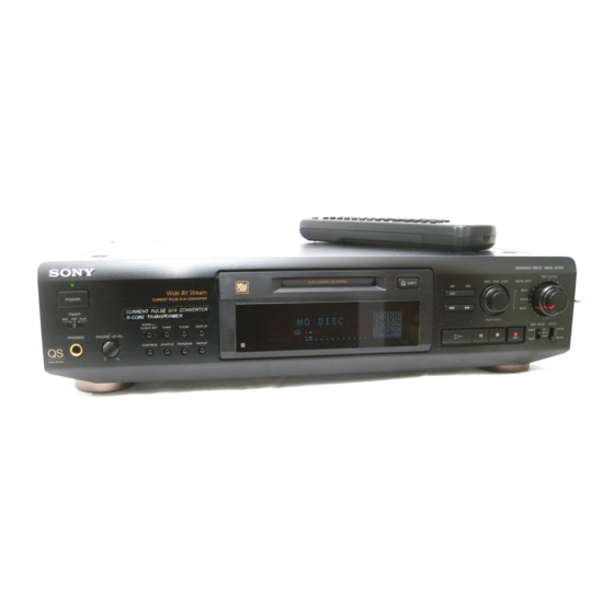
Sony MDS-JE700 - Mini Disc Player Service Manual
Minidisc deck
Hide thumbs
Also See for MDS-JE700 - Mini Disc Player:
- Operating instructions manual (40 pages) ,
- Limited warranty (1 page)
Table of Contents

Related Manuals for Sony MDS-JE700 - Mini Disc Player


Summary of Contents for Sony MDS-JE700 - Mini Disc Player
- Page 1 MDS-JE700 SERVICE MANUAL US Model Canadian Model AEP Model UK Model Model Name Using Similar Mechanism MDS-JE500 MD Mechanism Type MDM-3A Optical Pick-up Type KMS-260A/J1N SPECIFICATIONS — Continued on next page — MINIDISC DECK MICROFILM — 1 —...
- Page 2 CAUTION Danger of explosion if battery is incorrectly replaced. Replace only with the same or equivalent type recommended by the equipment manufacturer. Discard used batteries according to manufacture’s instructions. ADVARSEL! Lithiumbatteri - Eksplosionsfare ved fejlagtig håndtering. Udskiftning må kun ske med batteri af samme fabrikat og type. Levér det brugte batteri tilbage til leverandøren.
- Page 3 REPLACE THESE COMPONENTS WITH SONY PARTS FONCTIONNEMENT. NE REMPLACER CES COMPOSANTS WHOSE PART NUMBERS APPEAR AS SHOWN IN THIS QUE PAR DES PIÈCES SONY DONT LES NUMÉROS MANUAL OR IN SUPPLEMENTS PUBLISHED BY SONY. SONT DONNÉS DANS CE MANUEL OU DANS LES SUPPLÉMENTS PUBLIÉS PAR SONY.
-
Page 4: Table Of Contents
TABLE OF CONTENTS 1. SERVICING NOTE ............5 2. GENERAL ................8 3. DISASSEMBLY 3-1. Case and Front Panel Assembly .......... 24 3-2. Bracket (T), (L) and (R) ............24 3-3. BD Board ................25 3-4. SUB Chassis ................ 25 3-5. -
Page 5: Servicing Note
SECTION 1 SERVICING NOTE JIG FOR CHECKING BD BOARD WAVEFORM The special jig (J-2501-124-A) is useful for checking the waveform of the BD board. The names of terminals and the checking items to be performed are shown as follows. I+3V : For measuring IOP (Check the deterioration of the optical pick-up laser) IOP : For measuring IOP (Check the deterioration of the optical pick-up laser) TEO : TRK error signal (Traverse adjustment) : Reference level for checking the signal... - Page 6 RETRY CAUSE DISPLAY MODE • In this test mode, the causes for retry of the unit during recording can be displayed on the fluorescent display tube. This is useful for locating the faulty part of the unit. • The data amount stored in D RAM, number of retries, and retry cause are displayed. Each is displayed in hexadecimal number. •...
- Page 7 Reading the Retry Cause Display Higher Bits Lower Bits Hexa- Hexadecimal Cause of Retry Occurring conditions decimal b7 b6 b5 b4 b3 b2 b1 b0 Binary Spindle is slow When spindle rotation is detected as slow shock *1 When more than 3.5 shocks are detected When ADER was counted more than ader5 five times continuously...
-
Page 8: General
SECTION 2 GENERAL Location of Parts and Controls 2345 89 0 !¡ @¢ !ª !¶ !¢ @§ @∞ @£ @™ @¡ @º !• !§ !∞ !£ !™ 1 POWER switch !¢ r (recording) button 2 SCROLL/CLOCK SET button !∞ p (stop) button 3 CHAR button !§... - Page 9 This section is extracted from instruction manual. — 9 —...
- Page 10 — 10 —...
- Page 11 — 11 —...
- Page 12 — 12 —...
- Page 13 — 13 —...
- Page 14 — 14 —...
- Page 15 — 15 —...
- Page 16 — 16 —...
- Page 17 — 17 —...
- Page 18 — 18 —...
- Page 19 — 19 —...
- Page 20 — 20 —...
- Page 21 — 21 —...
- Page 22 — 22 —...
- Page 23 — 23 —...
-
Page 24: Disassembly
SECTION 3 DISASSEMBLY Follow the disassembly procedure in the numerical order given. Note : 3-1. CASE AND FRONT PANEL ASSEMBLY 7 Case 2 Screw (Case 3 TP2) 1 Two screws (Case 3 TP2) 6 Screw (BVTP3x8) 3 Screw (Case 3 TP2) 5 Screw (BVTP3x8) 9 Connector (6P) claw... -
Page 25: Bd Board
3-3. BD BOARD 2 Flat type wire (15 core) 4 OP relay flexible board 1 Flexible board (Over write head) 5 BD board 3 Screw (BVTT2x4) 3-4. SUB CHASSIS 1 Two step screws 2 Two step screws 3 Two insulators 4 Two insulators Part A Part A... -
Page 26: Shutter Assembly
3-5. SHUTTER ASSEMBLY 1 Stopper washer Shutter assembly Shaft (lid) 2 Shaft (shutter) 3 Shutter assembly Hole B Shaft (shutter) Hole A When installing, install the shaft (shutter) into the hole as shown in the figure before installing the shaft (lid) into the hole B. 3-6. -
Page 27: Slider Complete Assembly
3-7. SLIDER COMPLETE ASSEMBLY 3 Set the shaft of Gear (LB) to be at the claw position in the figure. claw 45° 4 Remove the slider complete assembly 1 Screw in the direction of arrow with putting (M1.7x2) 2 Retainer (gear) out of two claws. -
Page 28: Test Mode
SECTION 4 TEST MODE 4-1. PRECAUTIONS FOR USE OF TEST MODE 1 As loading related operations will be performed regardless of the test mode operations being performed, be sure to check that the disc is stopped before setting and removing it. Even if the §EJECT button is pressed while the disc is rotating during continuous playback, continuous recording, etc., the disc will not stop rotating. - Page 29 4-5-1. Operating the Continuous Playback Mode 1. Entering the continuous playback mode 1 Set the disc in the unit. (Whichever recordable discs or discs for playback only are available.) 2 Rotate the AMS knob and display “CPLAY MODE”. 3 Press the YES button to change the display to “CPLAY IN”. 4 When access completes, the display changes to “C1 = AD = ”.
- Page 30 4-6. FUNCTIONS OF OTHER BUTTONS Function Contents Sets continuous playback when pressed in the STOP state. When pressed during continuous playback, the tracking servo turns ON/OFF. Stops continuous playback and continuous recording. The sled moves to the outer circumference only when this is pressed. The sled moves to the inner circumference only when this is pressed.
-
Page 31: Electrical Adjustments
SECTION 5 ELECTRICAL ADJUSTMENTS 5-1. PRECAUTIONS FOR CHECKING LASER DIODE 5-3. PRECAUTIONS FOR ADJUSTMENTS EMISSINON 1) When replacing the following parts, perform the adjustments and checks with ¬ in the order shown in the following table. To check the emission of the laser diode during adjustments, never view directly from the top as this may lose your eye-sight. - Page 32 5-6. LASER PPOWER ADJUSTMENT 5-5. TEMPERATURE COMPENSATION OFFSET Connection : ADJUTMENT Laser power Save the temperature data at that time in the non-volatile memory meter as 25 ˚C reference data. Note : 1. Usually, do not perform this adjustment. 2. Perform this adjustment in an ambient temperature of 22 ˚C to Optical pick-up 28 ˚C.
- Page 33 5-7. TRAVERSE ADJUSTMENT 11. Rotate the AMS knob until the waveform of the oscilloscope moves closer to the specified value. Connection : In this adjustment, waveform varies at intervals of approx. 2%. Oscilloscope Adjust the waveform so that the specified value is satisfied as much as possible.
- Page 34 5-8. FOCUS BIAS ADJUSTMENT 5-9. ERROR RATE CHECK 5-9-1. CD Error Rate Check Adjusting Method : 1. Load a continuously recorded disc (Refer to “5-4. Creating Con- Checking Method : tinuously Recorded Disc”.). 1. Load a check disc (MD) TDYS-1. 2.
- Page 35 5-11. ADJUSTING POINTS AND CONNETING POINTS [BD BOARD] (SIDE A) 5 CN110 NOTE 1 + 3V CN101 D101 IC192 [BD BOARD] (SIDE B) IC171 IC101 IC121 NOTE : It is useful to use the jig. for checking the waveform. (Refer to Servicing Note on page 5.) —...
-
Page 36: Diagrams
SECTION 6 DIAGRAMS 6-1. CIRCUIT BOARDS LOCATION SW board AC board PANEL (L) board BD board MAIN board HP board DISPLAY board PANEL (R) board REC-VOL board — 36 —... -
Page 37: Bd Section
MDS-JE700 6-2. BLOCK DIAGRAMS — BD SECTION — DIGITAL SERVO SIGNAL PROCESSOR, DIGITAL SIGNAL PROCESSOR OVER WRITE HEAD DRIVE EFM/ACIRC ENCODER/DECODER, SHOCK-PROOF MEMORY CONTROLLER, IC181 ATRAC ENCODER/DECODER, 2M-BIT DRAM IC121 SCTX XINT Q180 HR901 • Signal path OVER WRITE HEAD : PB HEAD EFMO... -
Page 38: Main Section
MDS-JE700 DIGITAL DATA SELECTOR BUFFER IC356 IC355 — MAIN SECTION — DIGITAL IC353 OPTICAL IN1 A/D, D/A CONVERTER LINE AMP IC304 IC301 RV780 DIGITAL IC354 REC LEVEL INLM OPTICAL IN2 INLP ADDT J352 INRP CONVERTER DIGITAL INRM R-ch R-ch DIGITAL A A B B COAXIAL IN OPTICAL OUT... -
Page 47: Ic Block Diagrams
6-12. IC BLOCK DIAGRAMS IC101 CXA2523R 43 42 USROP – RF AGC – USRC RFA1 BPF3T RFA2 PEAK3T – HLPT –1 – – –2 – CFST PTGR TEMP PEAK – –2 – BOTTOM 36 BOTM – –1 – GRVA 35 ABCD 34 FE 33 AUX –... - Page 48 IC121 CXD2650R 100 99 98 97 96 95 94 93 92 91 90 89 88 87 86 85 84 83 82 81 80 79 78 77 76 75 AUX2 SPINDLE GENERATOR SERVO 74 TE MNT0 73 SE MNT1 MONITOR EACH 72 AVSS CONTROL BLOCK...
- Page 49 IC152 BH6511FS-E2 INTERFACE INTERFACE CHARGE PREDRIVE PREDRIVE PUMP. PREDRIVE PREDRIVE INTERFACE INTERFACE IC171 XL24C01AF-E2 1024 BIT EEPROM ARRAY 8BIT 7BIT ADDRESS SLAVE WORD DATA TEST 7BIT DECODER ADDRESS RESISTOR RESISTOR START STOP CONTROL CIRCUIT HIGH VOLTAGE VOLTAGE GENERATION CIRCUIT IC192 L88MS33T-TL START UP REFERENCE ERROR...
- Page 50 IC302 CXA8065S IC303 CXA8055M LINE02 LINE1 ANALOG CIREF RIREF PMUTE VOLUME REFERENCE VREF MIC1 CONTROL VOLTAGE LINE01 AGND VCNT CIRCUIT CIRCUIT SW01 – AGND MUTE IOR– LINE/MIC SWI1 – IOR+ CONSTANT CONSTANT IOL– –A/D1 CONTROL CONTROL CIRCUIT CIRCUIT +D/A1 IOL+ INV1 –...
- Page 51 IC351 LB1641 DRIVER INPUT LOGIC BLOCK OUT1 OUT2 IC356 SN74HC153AN DATA INPUTS STROBE OUTPUT SELECT STROBE 1C0 OUTPUT SELECT DATA INPUTS — 65 —...
- Page 52 IC901 LA5620 IC902 M5293L – REFERENCE VOLTAGE STBY REFERENCE ON/OFF – VOLTAGE OVERHEAT OVERCURRENT PROTECTION LIMITTER ANA5 – SYS3.3 – – 3.3V BACK – DELAY CIRCUIT P. DOWN – DELAY CIRCUIT VREF S. RESET — 66 —...
-
Page 53: Ic Pin Functions
6-13. IC PIN FUNCTIONS • IC101 RF Amplifier (CXA2523R) Pin No. Pin Name Function I-V converted RF signal I input I-V converted RF signal J input Middle point voltage (+1.5V) generation output 4 to 9 A to F Signal input from the optical pick-up detector Light amount monitor input Laser APC output APCREF... - Page 54 • IC121 Digital Signal Processor, Digital Servo Signal Processor, EFM/ACIRC Encoder/Decoder, Shock-proof Memory Controller, ATRAC Encoder/Decoder, 2M Bit DRAM (CXD2650R) Pin No. Pin Name Function FOK signal output to the system control MNT0 (FOK) “H” is output when focus is on MNT1 (SHCK) Track jump detection signal output to the system control MNT2 (XBUSY)
- Page 55 Pin No. Pin Name Function Data input/output for DRAM (Not used) D2, D3 48, 49 MVCI Clock input from an external VCO (Fixed at “L”) I (S) ASYO Playback EFM duplex signal output ASYI I (A) Playback EFM comparator slice level input AVDD +3V power supply (Analog) —...
- Page 56 Pin No. Pin Name Function Tracking servo drive PWM output (+) TFDR — +3V power supply (Digital) DVDD Focus servo drive PWM output (+) FFDR Focus servo drive PWM output (–) FRDR 176.4 kHz clock signal output (X’tal) (Not used) Sled servo drive PWM output (–) SRDR Sled servo drive PWM output (+)
- Page 57 • IC307 A/D, D/A converter (CXD8607N) Pin No. Pin Name Function INRP Rch analog (+) input INRM Rch analog (–) input REFI A/D reference voltage input (+3.2V) — +5V power supply (A/D, analog) AVss — Ground (A/D, analog) A/D analog block power down “L”: Power down —...
- Page 58 Pin No. Pin Name Function Lch PLM output 1 — +5V power supply (D/A, digital) — +5V power supply (A/D, digital) — — Ground (A/D, digital) TEST2 Test pin (Fixed at “L”) TEST3 — Ground (A/D, digital) SS1 (LF) — Not used —...
- Page 59 • IC401 System Control (RU8X11AMF-0113) Pin No. Pin Name Function Test pin. C1 is output when test mode (Not used) DAOUT 0 Test pin. ADER is output when test mode (Not used) DAOUT 1 Key input pin (D/A input) 3 to 5 KEY 0 to KEY 2 Detection input from the chucking-in switch “L”: Chucking CHUCK IN...
- Page 60 Pin No. Pin Name Function MNT2 Monitor 2 input from the CXD2650R MNT3 Monitor 3 input from the CXD2650R LED0 Drive output to the POWER ON/STANDBY display LED — Power supply ON: “H”, stand by: “L” — Not used CNTL A1 OUT CONTROL A1 signal output —...
- Page 61 Pin No. Pin Name Function DIG-RST Reset signal output to the CXD2650R and motor driver Reset: “L” BEEP PWM output (Not used) BEEP Reset signal output to the D/A, A/D converter Reset: “L” DA-RST Digital input selection signal output 84, 85 DSEL A, DSEL B Laser modulation switching signal output Playback power: “L”, stop: “H”...
-
Page 62: Exploded Views
SECTION 7 EXPLODED VIEWS NOTE: • Items marked “*” are not stocked since they are • Hardware (# mark) list and accessories and pack- The components identified by mark ! seldom required for routine service. Some delay ing materials are given in the last of this parts list. or dotted line with mark ! are critical should be anticipated when ordering these items. -
Page 63: Front Panel Section
Description Remark Ref. No. Part No. Description Remark 4-985-442-11 PANEL, FRONT 4-951-620-01 SCREW (2.6X8), +BVTP 4-979-587-01 EMBLEM (NO.5), SONY * 66 1-663-116-11 REC-VOL BOARD 4-985-454-01 INDICATOR (B) 4-985-449-11 BUTTON (EDIT) 4-950-189-01 KNOB (A)(VOL) 4-985-447-11 BUTTON (MODE) X-4947-592-1 BASE ASSY, PANEL... -
Page 64: Mechanism Deck Section (1) (Mdm-3A)
7-3. MECHANISM DECK SECTION (1) (MDM-3A) not supplied not supplied not supplied not supplied not supplied Ref. No. Part No. Description Remark Ref. No. Part No. Description Remark 4-628-167-01 SCREW, STEP 1-660-966-11 OP RELAY FLEXIBLE BOARD 4-987-327-01 INSULATOR * 207 A-4699-092-A BD BOARD, COMPLETE 4-986-959-01 WASHER, STOPPER 1-777-517-11 WIRE (FLAT TYPE)(15 CORE) -
Page 65: Mechanism Deck Section (2) (Mdm-3A)
7-4. MECHANISM DECK SECTION (2) (MDM-3A) not supplied not supplied not supplied M901 M903 M902 HR901 Les composants identifiés par The components identified by mark ! or dotted line with mark une marque ! sont critiques pour ! are critical for safety. la sécurité. -
Page 66: Electrical Parts List
SECTION 8 ELECTRICAL PARTS LIST Note: • Due to standardization, replacements in the parts list • SEMICONDUCTORS The components identified by mark ! may be different from the parts specified in the In each case, u: µ , for example: or dotted line with mark ! are critical diagrams or the components used on the set. - Page 67 Ref. No. Part No. Description Remark Ref. No. Part No. Description Remark C188 1-164-232-11 CERAMIC CHIP 0.01uF Q182 8-729-017-65 TRANSISTOR 2SK1764KY C189 1-163-989-11 CERAMIC CHIP 0.033uF C190 1-126-206-11 ELECT CHIP 100uF 6.3V < RESISTOR > C191 1-163-038-91 CERAMIC CHIP 0.1uF C195 1-164-346-11 CERAMIC CHIP R101...
- Page 68 DISPLAY MAIN Ref. No. Part No. Description Remark Ref. No. Part No. Description Remark R734 1-247-807-31 CARBON 1/4W R179 1-216-089-91 METAL GLAZE 1/10W R180 1-216-073-00 METAL CHIP 1/10W R741 1-249-401-11 CARBON 1/4W F R742 1-247-807-31 CARBON 1/4W R181 1-216-073-00 METAL CHIP 1/10W R182 1-216-089-91 METAL GLAZE...
- Page 69 MAIN Ref. No. Part No. Description Remark Ref. No. Part No. Description Remark < CAPACITOR > C322 1-126-335-11 ELECT 220uF C323 1-162-205-31 CERAMIC 18PF C101 1-130-467-00 MYLAR 470PF C324 1-162-205-31 CERAMIC 18PF C102 1-124-673-11 ELECT 100uF C325 1-126-335-11 ELECT 220uF C103 1-124-721-11 ELECT 10uF...
- Page 70 MAIN Ref. No. Part No. Description Remark Ref. No. Part No. Description Remark < TRANSISTOR > < CONNECTOR > Q101 8-729-141-30 TRANSISTOR 2SC3623A-LK * CN301 1-564-708-11 PIN, CONNECTOR (SMALL TYPE) 6P Q201 8-729-141-30 TRANSISTOR 2SC3623A-LK * CN302 1-564-708-11 PIN, CONNECTOR (SMALL TYPE) 6P Q301 8-729-422-61 TRANSISTOR UN4115 CN303...
- Page 71 MAIN PANEL (L) Ref. No. Part No. Description Remark Ref. No. Part No. Description Remark R213 1-249-408-11 CARBON 1/4W F R412 1-249-441-11 CARBON 100K 1/4W R214 1-249-408-11 CARBON 1/4W F R215 1-249-411-11 CARBON 1/4W R413 1-249-441-11 CARBON 100K 1/4W R216 1-249-411-11 CARBON 1/4W R414...
- Page 72 PANEL (L) PANEL (R) REC-VOL Ref. No. Part No. Description Remark Ref. No. Part No. Description Remark R756 1-249-421-11 CARBON 2.2K 1/4W F R713 1-249-435-11 CARBON 1/4W R714 1-249-421-11 CARBON 2.2K 1/4W F R757 1-249-429-11 CARBON 1/4W R715 1-249-429-11 CARBON 1/4W R758 1-249-421-11 CARBON...
- Page 73 Ref. No. Part No. Description Remark MISCELLANEOUS ************** 1-777-278-11 WIRE (FLAT TYPE)(19 CORE) 1-777-275-11 WIRE (FLAT TYPE)(29 CORE) ! 12 1-558-568-21 CORD, POWER (AEP) ! 12 1-559-583-21 CORD, POWER (US,CND) ! 12 1-696-586-11 CORD, POWER (UK) 1-777-846-11 WIRE (FLAT TYPE)(23 CORE) 1-660-966-11 OP RELAY FLEXIBLE BOARD 1-777-517-11 WIRE (FLAT TYPE)(15 CORE) ! 267...
- Page 74 MDS-JE700 Sony Corporation 97B0977-1 9-960-804-11 Printed in Japan © 1997. 2 Home A&V Products Company Published by Service and Safety — 88 — Engineering Dept. (Shibaura)